

Compact, 1.5 A Linear Charger
4
FEATURES
Simple, safe linear charger for single cell lithium battery
4.5 V to 12 V input voltage range
Adjustable charging current up to 1.5 A
Low cost PNP external pass element
Automatic reverse isolation with no external blocking diode
Output overshoot protection
Deep discharge precharge mode
Thermal shutdown
Automatic recharge
Programmable termination timer
LED charging status indicator
4.2 V output voltage with ±1% accuracy over line and
temperature
1 µA shutdown supply current
Small, 8-pin MSOP and 3 × 3 mm LFCSP packages
APPLICATIONS
Wireless handsets
Smart handhelds and PDAs
Digital cameras
Single cell lithium ion-powered systems
Cradle chargers
for Single-Cell Li+ Battery
ADP2291
GENERAL DESCRIPTION
The ADP2291 is a constant-current/constant-voltage linear
charger for a single cell lithium ion battery, requiring just a few
components to provide a simple and safe charging system that
operates from a wide 4.5 V to 12 V input voltage range. It
features an internally controlled, multistep charging cycle that
improves battery life.
An external, low cost, PNP provides the charging current to the
battery and an external resistor sets the maximum charge
current. A small external capacitor programs the maximum
charge time. The controller includes an LED driver to indicate
the battery charging status.
Safety features include charging stop mode for battery faults,
output overshoot protection, and thermal shutdown. The
ADP2291 also features automatic reverse isolation, which does
not require an additional blocking diode.
The multistep charge cycle optimizes the battery charging time
in a safe manner. It features a trickle charge mode for a deeply
discharged cell and a fast charging mode with a maximum
current of 1.5 A. The ADP2291 controls the end of charge with
a 4.2 V output voltage that is 1% accurate over line and temperature. It automatically recharges the battery if the cell voltage
drops. When the input supply is removed, the part enters a low
current state and reduces the current drawn from the battery to
below 1 µA.
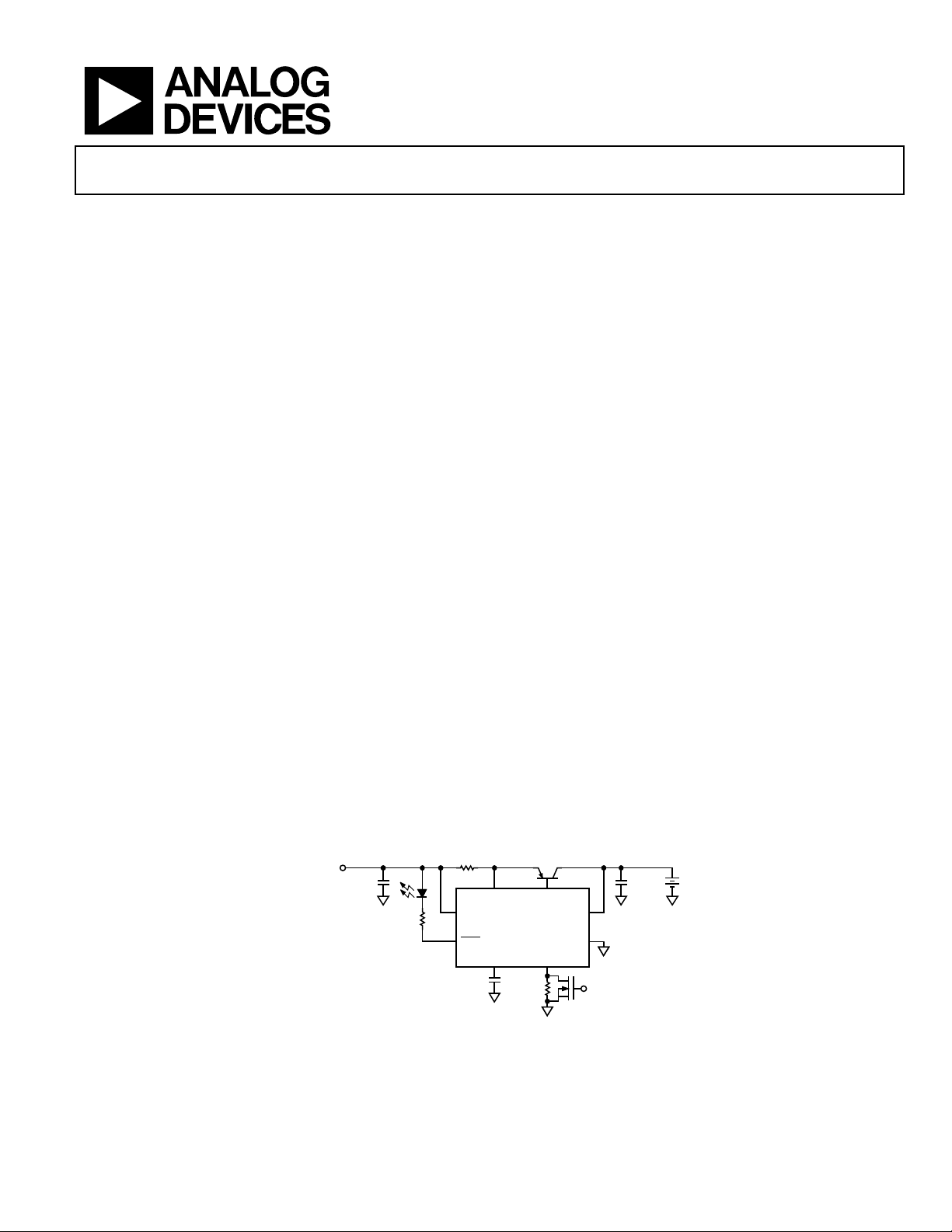
TYPICAL OPERATING CIRCUIT
INPUT
.6V–12V
Rev. 0
Information furnished by Analog Devices is believed to be accurate and reliable.
However, no responsibility is assumed by Analog Devices for its use, nor for any
infringements of patents or other rights of third parties that may result from its use.
Specifications subject to change without notice. No license is granted by implication
or otherwise under any patent or patent rights of Analog Devices. Trademarks and
registered trademarks are the property of their respective owners.
CIN
CTIMER
Figure 1. Basic Circuit Configuration
The ADP2291 is available in both a small, 8-pin MSOP package
and a 3 × 3 mm LFCSP package that is ideally suited for small,
portable applications.
RS Q1
CS DRV
IN
ADP2291
CHG
TIMER ADJ
One Technology Way, P.O. Box 9106, Norwood, MA 02062-9106, U.S.A.
Tel: 781.329.4700
Fax: 781.326.8703 © 2004 Analog Devices, Inc. All rights reserved.
+
COUT
BAT
GND
SHUTDOWN
04873-0-001
www.analog.com

ADP2291
TABLE OF CONTENTS
Specifications..................................................................................... 3
Absolute Maximum Ratings............................................................ 5
ESD Caution.................................................................................. 5
Pin Configuration And Functional Descriptions......................... 6
Typical Performance Characteristics............................................. 7
Theory of Operation ...................................................................... 10
Precharge Mode.......................................................................... 10
End-of-Charge Mode................................................................. 10
Shutdown Mode.......................................................................... 10
Charge Restart............................................................................. 10
Programmable Timer................................................................. 10
Charge Status Indicator ............................................................. 10
Automatic Reverse Isolation ..................................................... 10
Overshoot Protection................................................................. 10
Power Supply Checks ................................................................. 10
Thermal Shutdown .................................................................... 11
Application Information................................................................ 12
Setting the Maximum Charge Current.................................... 12
Setting the Maximum Charge Time ........................................ 12
External Capacitors.................................................................... 12
Reverse Input Protection ........................................................... 12
External Pass Transistor ............................................................ 13
Typical Application Circuit ....................................................... 14
EOC Terminates Charging........................................................ 14
Selectable Charge Current......................................................... 14
Thermal Protection .................................................................... 14
Printed Circuit Board Layout Considerations........................ 16
LFSCP Layout Considerations.................................................. 16
Outline Dimensions....................................................................... 18
Ordering Guide .......................................................................... 18
REVISION HISTORY
10/04—Initial Version: Revision 0
Rev. 0 | Page 2 of 20

ADP2291
SPECIFICATIONS
VIN = 5.5 V, V
= 4.2 V, R
BAT
open, TA = –40°C to +85°C, typical values are at 25°C unless otherwise noted.
ADJ
Table 1. Electrical Characteristics
Parameter Conditions Min Typ Max Unit
Power Supply, IN
Input Voltage 4.5 12 V
Current Draw
Fast charge/precharge/end-of-charge modes
Timeout/shutdown/battery fault
Battery Voltage, BAT
Voltage Accuracy, End-of-charge (V
Load Regulation, No Battery VIN – VCS = 0 to VRS
Current Draw
Current Draw
Reverse Leakage Current
BAT, EOC
)
= 0°C to +50°C
T
A
= 4.5 V to 12 V
V
IN
V
– VCS = VRS/10
IN
Timeout mode
= 4.5 V to 12 V
V
IN
Battery fault/shutdown mode
= 4.5 V to 12 V
V
IN
Power-down mode
= float, V
V
IN
BAT
= 4.2 V
Fast Charge Mode
Sense Voltage Setpoint (VRS)
Sense Voltage Setpoint (VRS)
Current Regulation Adjustment per V of (3 V – V
– VCS, R
V
IN
V
IN
V
BAT
V
IN
V
IN
V
BAT
ADJ
= 4.5 V to 12 V
= 3.6 V
– VCS, R
ADJ
= 4.5 V to 12 V
= 3.6 V
= open
= 100 kΩ
) 67 mV/V
ADJ
Precharge Mode
Sense Voltage Setpoint (VRS)
Sense Voltage Setpoint (VRS)
BAT Precharge Threshold V
– V
V
IN
= 4.5 V to 12 V
V
IN
V
= 2 V
BAT
– VCS, R
V
IN
V
= 4.5 V to 12 V
IN
= 2 V
V
BAT
rising 2.65 2.85 V
BAT
CS, RADJ
ADJ
= open
= 100 kΩ
Hysteresis 70 mV
Shutdown Mode
ADJ Shutdown Threshold V
falling, VIN = 4.5 V 0.30 0.45 V
ADJ
Hysteresis 40 mV
Pullup current from ADJ V
= 0 40 µA
ADJ
Power-Down Mode
VIN Powerdown Threshold VIN rising 3.6 4 V
Hysteresis 220 mV
VIN_Good Comparator
Threshold (VIN > V
) VIN rising 125 170 220 mV
BAT
Hysteresis 110 mV
EOC Comparator
Current Threshold VIN – VCS falling, R
Current Threshold VIN – VCS falling, R
= open, relative to VRS 7 10 13 %
ADJ
= 100 kΩ, relative to VRS 6 10 16 %
ADJ
Hysteresis 12 mV
Restart Comparator
BAT Restart Threshold VIN > 4.5 V, V
falling, relative to V
BAT
BAT, EOC
1
6
1.4 9 1.8
mA
mA
4.158 4.2 4.242 V
–80 mV
45 µA
0.1 1 µA
0.1 µA
140 150 160 mV
40 50 60 mV
10 15 20 mV
5 10 15 mV
–170 mV
Rev. 0 | Page 3 of 20

ADP2291
Parameter Conditions Min Typ Max Unit
Battery Charge Timer
Charge/Discharge TIMER Current 21.0 24.0 27.0 µA
Low Threshold 1.2 V
High Threshold 2.0 V
High-Low Threshold Delta
Overshoot Protection
BAT Threshold 4.7 5 5.3 V
Current Sink <2 ms duration 1.5 A
CHG Output
Output Voltage Low Current = 20 mA 0.45 V
Output Leakage Current V
Base Drive Capability
Max Base Drive Current 40 mA
Thermal Shutdown
Shutdown Threshold TA rising 135 °C
Hysteresis 35 °C
1
All limits at temperature extremes are guaranteed via correlation using standard statistical quality control (SQC). Typical values are at TA = 25° C.
2
Guaranteed by design, not tested in production.
2
750 850 mV
= 5 V 0.1 1 µA
CHG
Rev. 0 | Page 4 of 20

ADP2291
ABSOLUTE MAXIMUM RATINGS
Table 2.
Parameter Rating
IN, DRV1, CS, CHG, to GND
BAT, ADJ, TIMER to GND −0.3 V to (VIN + 0.3 V)
Operating Ambient Temperature −40°C to +85°C
Operating Junction Temperature −40°C to +125°C
θJA, 2-layer MSOP-8 220ºC/W
θJA, 4-layer MSOP-8 158ºC/W
θJA, 2-layer LFCSP-8 62ºC/W
θJA, 4-layer LFCSP-8 48ºC/W
Storage Temperature −65°C to +150°C
Lead Temperature Range Soldering
(10 sec)
−0.3 V to +13.5 V
300°C
ESD CAUTION
ESD (electrostatic discharge) sensitive device. Electrostatic charges as high as 4000 V readily accumulate on
the human body and test equipment and can discharge without detection. Although this product features
proprietary ESD protection circuitry, permanent damage may occur on devices subjected to high energy
electrostatic discharges. Therefore, proper ESD precautions are recommended to avoid performance
degradation or loss of functionality.
Stresses above those listed under Absolute Maximum Ratings
may cause permanent damage to the device. This is a stress
rating only and functional operation of the device at these or
any other condition s above those indicated in the operational
section of this specification is not implied. Exposure to absolute
maximum rating conditions for extended periods may affect
device reliability. Absolute maximum ratings apply individually
only, not in combination. Unless otherwise specified all other
voltages referenced to GND.
1
Pulling current from the DRV pin by driving it below ground, while VIN is
applied, may cause permanent damage to the device.
Rev. 0 | Page 5 of 20

ADP2291
PIN CONFIGURATION AND FUNCTIONAL DESCRIPTIONS
DRV
1
CS
ADP2291
2
TOP VIEW
3
(Not to Scale)
4
GND
BAT
Figure 2. 8-Lead MSOP
Table 3. Pin Function Descriptions
Pin No. Mnemonic Description
1 DRV Base Driver Output. Controls the base of an external PNP pass transistor.
2 GND Ground.
3 BAT Battery Voltage Sense Input.
4 CS Current Sense Resistor Negative Input.
5 ADJ Charging Current Adjust and Charger Shutdown Input.
6 IN Power Input and Current-Sense Resistor Positive Input.
7 TIMER Timer Programming Input/Disable.
8
CHG
CHG
8
TIMER
7
6
IN
ADJ
5
04873-0-002
LED Charge-Status Indicator. This is an open-collector output.
PIN 1
1DRV
INDICATOR
2GND
ADP2291
3BAT
TOP VIEW
(Not to Scale)
4CS
Figure 3. 8-Lead LFCSP
8 CHG
7 TIMER
6IN
5 ADJ
04873-0-003
Rev. 0 | Page 6 of 20
 Loading...