ANALOG DEVICES ADP222, ADP223, ADP224, ADP225 Service Manual
High PSRR Voltage Regulators
ADP222/ADP223/ADP224/ADP225
Rev. B
Trademarks and registered trademarks are the property of their respective owners.
Fax: 781.461.3113 ©2011 Analog Devices, Inc. All rights reserved.
EN1
VOUT1
VIN
EN2
GND
6
4
3
2
ADJ2 VOUT2
1
8
5
7
ADJ1
ADP223/
ADP225
R1
R4
R2
ON
OFF
ON
OFF
V
IN
= 4.2V
+
C1
1µF
+
C3
1µF
+
C2
1µF
VOUT1 = 2. 8V
VOUT2 = 2. 0V
09376-001
R3
EN1
VOUT1
VIN
EN2
GND
6
4
3
2
SENSE2 VOUT2
1 8
5
7
SENSE1
ADP222/
ADP224
ON
OFF
ON
OFF
V
IN
= 4.2V
+
C1
1µF
+
C3
1µF
+
C2
1µF
VOUT2 = 3.3V
VOUT1 = 1.5V
09376-101
Data Sheet
FEATURES
Input voltage range: 2.5 V to 5.5 V
Small, 8-lead, 2 mm × 2 mm LFCSP package
Initial accuracy: ±1%
High PSRR: 70 dB at 10 kHz, 60 dB at 100 kHz, 40 dB at 1 MHz
Low noise: 27 µV rms at V
Excellent transient response
Low dropout voltage: 170 mV at 300 mA load
65 µA typical ground current at no load, both LDOs enabled
Fixed output voltage from 0.8 V to 3.3 V (ADP222/ADP224)
Adjustable output voltage range from 0.5 V to 5.0 V
(ADP223/ADP225)
Quick output discharge (QOD)—ADP224/ADP225
Overcurrent and thermal protection
APPLICATIONS
Portable and battery-powered equipment
Portable medical devices
Post dc-to-dc regulation
Point of sale terminals
Credit card readers
Automatic meter readers
Wireless network equipment
= 1.2 V, 50 µV rms at V
OUT
= 2.8 V
OUT
Dual, 300 mA Output, Low Noise,
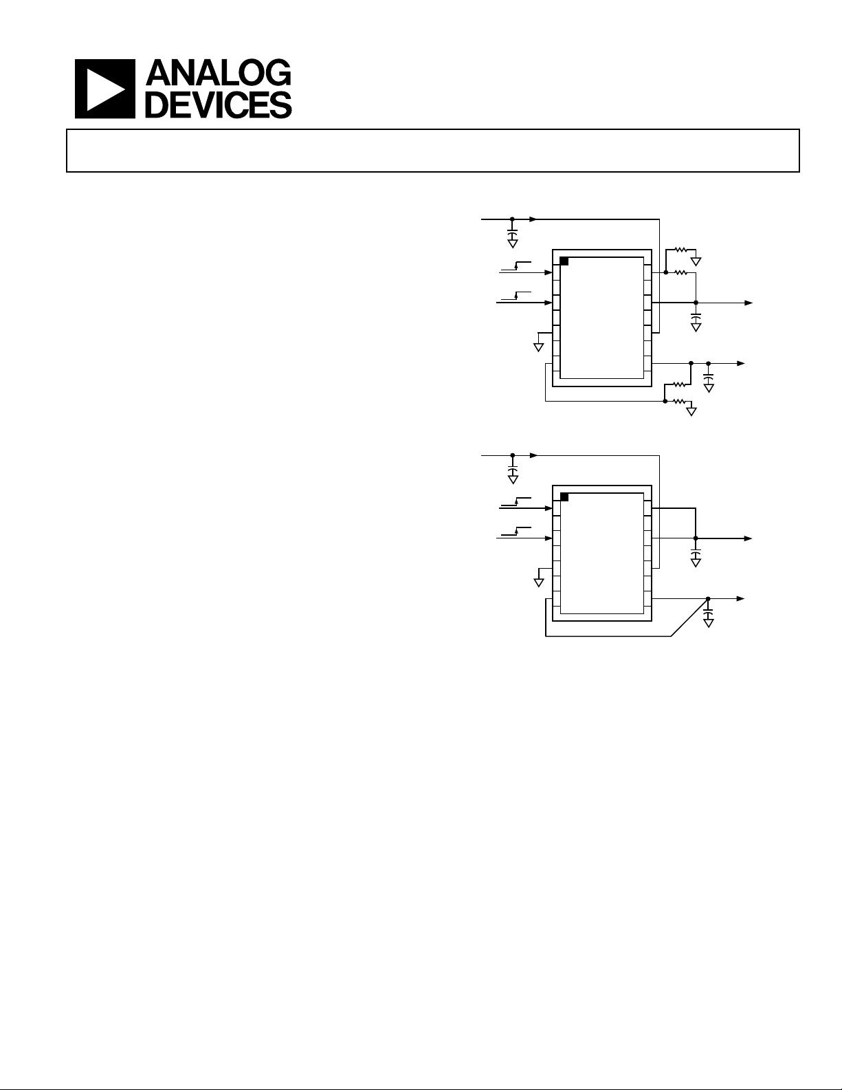
TYPICAL APPLICATION CIRCUITS
Figure 1. ADP223/ADP225
GENERAL DESCRIPTION
The 300 mA, adjustable dual output ADP223/ADP225 and
fixed dual output ADP222/ADP224 combine high PSRR, low
noise, low quiescent current, and low dropout voltage in a
voltage regulator that is ideally suited for wireless applications
with demanding performance and board space requirements.
The ADP222/ADP224 are available with fixed outputs voltages
from 0.8V to 3.3V. The adjustable output ADP223/ADP225 may
be set to output voltages from 0.5 V to 5.0 V. The low quiescent
current, low dropout voltage, and wide input voltage range of
the ADP222/ADP223/ADP224/ADP225 extend the battery life
of portable devices.
The ADP222/ADP223/ADP224/ADP225 maintain power
supply rejection greater than 60 dB for frequencies as high as
Information furnished by Analog Devices is believed to be accurate and reliable. However, no
responsibility is assumed by Analog Devices for its use, nor for any infringements of patents or other
rights of third parties that may result from its use. Specifications subject to change without notice. No
license is granted by implication or otherwise under any patent or patent rights of Analog Devices.
Figure 2. ADP222/ADP224
100 kHz while operating with a low headroom voltage. The
ADP222/ADP223/ADP224/ADP225 offer much lower noise
performance than competing LDOs without the need for a
noise bypass capacitor. Overcurrent and thermal protection
circuitry prevent damage in adverse conditions.
The ADP224 and ADP225 are identical to the ADP222 and
ADP223, respectively, but with the addition of a quick output
discharge (QOD) feature.
The ADP222/ADP223/ADP224/ADP225 are available in a
small 8-lead, 2 mm × 2 mm LFCSP package and are stable with
tiny 1 µF, ±30% ceramic output capacitors, resulting in the smallest
possible board area for a wide variety of portable power needs.
One Technology Way, P.O. Box 9106, Norwood, MA 02062-9106, U.S.A.
Tel: 781.329.4700
www.analog.com

ADP222/ADP223/ADP224/ADP225 Data Sheet
TABLE OF CONTENTS
Features .............................................................................................. 1
Applications ....................................................................................... 1
Typical Application Circuits ............................................................ 1
General Description ......................................................................... 1
Revision History ............................................................................... 2
Specifications ..................................................................................... 3
Input and Output Capacitor, Recommended Specifications .. 4
Absolute Maximum Ratings ............................................................ 5
Thermal Data ................................................................................ 5
Thermal Resistance ...................................................................... 5
ESD Caution .................................................................................. 5
Pin Configuration and Function Descriptions ............................. 6
REVISION HISTORY
8/11—Rev. A to Rev. B
Changes to Features and General Descriptions Sections ............ 1
Added Figure 64; Renumbered Sequentially .............................. 17
Changes to Theory of Operation Section .................................... 17
Changes to Output Capacitor Section ......................................... 18
Changes to Paralleling Outputs to Increase Output
Current Section ............................................................................... 19
Updated Outline Dimensions ....................................................... 23
Typical Performance Characteristics ..............................................7
Theory of Operation ...................................................................... 17
Applications Information .............................................................. 18
Capacitor Selection .................................................................... 18
Enable Feature ............................................................................ 19
Paralleling Outputs to Increase Output Current .................... 19
Quick Output Discharge (QOD) Function ............................ 19
Current Limit and Thermal Overload Protection ................. 20
Thermal Considerations ............................................................ 20
Printed Circuit Board Layout Considerations........................ 22
Outline Dimensions ....................................................................... 23
Ordering Guide .......................................................................... 23
7/11—Rev. 0 to Rev. A
Added ADP222, ADP224, and ADP225 ......................... Universal
Changes to Features Section, Applications Section,
General Description Section, and Figure 2 .................................... 1
Changes to Table 1 ............................................................................. 3
Added Figure 4; Renumbered Sequentially ................................... 6
Changes t o Table 5 ............................................................................. 6
Changes to Typical Performance Characteristics Section ........... 7
Changes to Theory of Operation Section and Figure 62 .......... 17
Added Figure 63 ............................................................................. 17
Added Quick Output Discharge (QOD) Function Section
Added Figure 70 ............................................................................. 20
2/11—Revision 0: Initial Version
Rev. B | Page 2 of 24

Data Sheet ADP222/ADP223/ADP224/ADP225
INPUT VOLTAGE RANGE
VIN
TJ = −40°C to +125°C
2.5 5.5
V
V
= 0.8 V
100 µs
EN Input Leakage Current
V
EN1 = EN2 = VIN or GND
0.1 µA
UNDERVOLTAGE LOCKOUT
UVLO
Input Voltage Rising
UVLO
2.45
V
SPECIFICATIONS
VIN = (V
unless otherwise noted.
Table 1.
Parameter Symbol Test Conditions/Comments Min Typ Max Unit
+ 0.5 V) or 2.5 V (whichever is greater), EN1 = EN2 = VIN, I
OUT
OUT1
= I
= 10 mA, CIN = C
OUT2
OUT1
= C
= 1 µF, TA = 25°C,
OUT2
OPERATING SUPPLY CURRENT
I
I
GND
= 0 µA 65 µA
OUT
WITH BOTH REGULATORS ON
I
I
I
I
I
SHUTDOWN CURRENT I
OUTPUT VOLTAGE ACCURACY1 V
EN1 = EN2 = GND 0.2 2 µA
GND-SD
TJ = −40°C to +125°C
OUT
I
0 µA < I
ADJUSTABLE-OUTPUT VOLTAGE
ACCURACY
1
TJ = −40°C to +125°C
V
ADJ
I
0 µA < I
LINE REGULATION ΔV
/ΔVIN VIN = (V
OUT
VIN = (V
LOAD REGULATION2 ΔV
OUT
/ΔI
OUT
I
DROPOUT VOLTAGE3 V
DROPOUT
I
I
I
SENSE INPUT BIAS CURRENT SENSE
ADJx INPUT BIAS CURRENT ADJ
START-UP TIME4 t
CURRENT-LIMIT THRESHOLD5 I
I-BIAS
2.5 V ≤ VIN ≤ 5.5 V, ADJx connected to VOUTx 10 nA
I-BIAS
V
STA RT-UP
340 400 mA
LIMIT
= 0 µA, TJ = −40°C to +125°C 150 µA
OUT
= 10 mA 100 µA
OUT
= 10 mA, TJ = −40°C to +125°C 200 µA
OUT
= 300 mA 300 µA
OUT
= 300 mA, TJ = −40°C to +125°C 450 µA
OUT
= 10 mA −1 +1 %
OUT
< 300 mA, VIN = (V
OUT
= 10 mA 0.495 0.500 0.505 V
OUT
< 300 mA, VIN = (V
OUT
+ 0.5 V) to 5.5 V 0.01 %/V
OUT
+ 0.5 V ) to 5.5 V, TJ = −40°C to +125°C −0.05 +0.05 %/V
OUT
I
= 1 mA to 300 mA 0.001 %/mA
OUT
= 1 mA to 300 mA, TJ = −40°C to +125°C 0.002 %/mA
OUT
V
= 3.3 V
OUT
I
= 10 mA 6 mV
OUT
= 10 mA, TJ = −40°C to +125°C 9 mV
OUT
= 300 mA 170 mV
OUT
= 300 mA, TJ = −40°C to +125°C A 260 mV
OUT
+ 0.5 V) to 5.5 V −2 +2 %
OUT
+ 0.5 V) to 5.5 V 0.490 0.510 V
OUT
2.5 V ≤ VIN ≤ 5.5 V, SENSEx connected to VOUTx 10 nA
= 3.3 V 240 µs
OUT
OUT
THERMAL SHUTDOWN
Thermal Shutdown Threshold TSSD TJ rising 155 °C
Thermal Shutdown Hysteresis TS
15 °C
SD-HYS
EN INPUT
EN Input Logic High VIH 2.5 V ≤ VIN ≤ 5.5 V 1.2 V
EN Input Logic Low VIL 2.5 V ≤ VIN ≤ 5.5 V 0.4 V
I-LEAKAGE
EN1 = EN2 = VIN or GND, TJ = −40°C to +125°C 1 µA
Input Voltage Falling UVLO
Hysteresis UVLO
OUTPUT DISCHARGE TIME t
OUTPUT DISCHARGE RESISTANCE R
RISE
2.2 V
FAL L
HYS
V
DIS
140 Ω
QOD
= 2.8 V 1000 µs
OUT
Rev. B | Page 3 of 24
120
mV
ADP222/ADP223/ADP224/ADP225 Data Sheet
10 kHz
68 dB
Parameter Symbol Test Conditions/Comments Min Typ Max Unit
OUTPUT NOISE OUT
10 Hz to 100 kHz, VIN = 5 V, V
10 Hz to 100 kHz, VIN = 3.6 V, V
10 Hz to 100 kHz, VIN = 3.6 V, V
POWER SUPPLY REJECTION RATIO PSRR VIN = 2.5 V, V
100 Hz 76 dB
1 kHz 76 dB
10 kHz 70 dB
100 kHz 60 dB
1 MHz 40 dB
VIN = 3.8 V, V
100 Hz 68 dB
1 kHz 68 dB
100 kHz 60 dB
1 MHz 40 dB
1
Accuracy when VOUTx is connected directly to ADJx or SENSEx. When the VOUTx voltage is set by external feedback resistors, the absolute accuracy in adjust mode
depends on the tolerances of resistors used.
2
Based on an end-point calculation using 1 mA and 300 mA loads.
3
Dropout voltage is defined as the input-to-output voltage differential when the input voltage is set to the nominal output voltage. This applies only for output
voltages above 2.5 V.
4
Start-up time is defined as the time between the rising edge of EN to V
5
Current-limit threshold is defined as the current at which the output voltage drops to 90% of the specified typical value. For example, the current limit for a 3.0 V
output voltage is defined as the current that causes the output voltage to drop to 90% of 3.0 V or 2.7 V.
10 Hz to 100 kHz, VIN = 5 V, V
NOISE
= 0.8 V, I
OUT
= 2.8 V, I
OUT
being at 90% of its nominal value.
OUT
= 3.3 V 56 µV rms
OUT
= 2.8 V 50 µV rms
OUT
= 2.5 V 45 µV rms
OUT
= 1.2 V 27 µV rms
OUT
= 100 mA
OUT
= 100 mA
OUT
INPUT AND OUTPUT CAPACITOR, RECOMMENDED SPECIFICATIONS
The minimum input and output capacitance should be greater than 0.70 µF over the full range of the operating conditions. The full range of the
operating conditions in the application must be considered during device selection to ensure that the minimum capacitance specification
is met. X7R and X5R type capacitors are recommended for use with the LDOs, but Y5V and Z5U capacitors are not recommended for use
with the LDOs.
Table 2.
Parameter Symbol Conditions Min Typ Max Unit
MINIMUM INPUT AND OUTPUT CAPACITANCE C
CAPACITOR ESR R
TA = −40°C to +125°C 0.70 µF
MIN
TA = −40°C to +125°C 0.001 1 Ω
ESR
Rev. B | Page 4 of 24
Data Sheet ADP222/ADP223/ADP224/ADP225
ABSOLUTE MAXIMUM RATINGS
Table 3.
Parameter Rating
VIN to GND −0.3 V to +6 V
ADJ1, ADJ2, VOUT1, VOUT2 to GND −0.3 V to VIN
EN1, EN2 to GND −0.3 V to +6 V
Storage Temperature Range −65°C to +150°C
Operating Junction Temperature Range −40°C to +125°C
Soldering Conditions JEDEC J-STD-020
Stresses above those listed under Absolute Maximum Ratings
may cause permanent damage to the device. This is a stress
rating only; functional operation of the device at these or any
other conditions above those indicated in the operational
section of this specification is not implied. Exposure to absolute
maximum rating conditions for extended periods may affect
device reliability.
THERMAL DATA
Absolute maximum ratings apply individually only, not in
combination.
The ADP222/ADP223/ADP224/ADP225 can be damaged when
the junction temperature limits are exceeded. Monitoring
ambient temperature does not guarantee that T
specified temperature limits. In applications with high power
dissipation and poor thermal resistance, the maximum ambient
temperature may have to be derated. In applications with
moderate power dissipation and low PCB thermal resistance, the
maximum ambient temperature can exceed the maximum limit as
long as the junction temperature is within specification limits.
The junction temperature (T
ambient temperature (T
(P
), and the junction-to-ambient thermal resistance of the
D
package (θ
). Maximum junction temperature (TJ) is calculated
JA
from the ambient temperature (T
) of the device is dependent on the
J
), the power dissipation of the device
A
) and power dissipation (PD)
A
using the formula
T
= TA + (PD × θJA)
J
is within the
J
Junction-to-ambient thermal resistance (θ
based on modeling and calculation using a 4-layer board. θ
is highly dependent on the application and board layout. In
applications where high maximum power dissipation exists,
close attention to thermal board design is required. The value
of θ
may vary, depending on PCB material, layout, and
JA
environmental conditions. The specified value of θ
on a 4-layer, 4 in × 3 in, 2½ oz copper board, as per JEDEC
standards. For more information, see the AN-772 Application
Note, A Design and Manufacturing Guide for the Lead Frame
Chip Scale Package (LFCSP).
Ψ
is the junction-to-board thermal characterization parameter
JB
with units of °C /W. Ψ
of the package is based on modeling and
JB
calculation using a 4-layer board. The JESD51-12, Guidelines for
Reporting and Using Package Thermal Information, states that
thermal characterization parameters are not the same as thermal
resistances. Ψ
measures the component power flowing
JB
through multiple thermal paths rather than a single path as in
thermal resistance, θ
. Therefore, ΨJB thermal paths include
JB
convection from the top of the package as well as radiation from
the package, factors that make Ψ
more useful in real-world
JB
applications. Maximum junction temperature (T
from the board temperature (T
) and power dissipation (PD)
B
using the formula
T
= TB + (PD × ΨJB)
J
Refer to JESD51-8 and JESD51-12 for more detailed
information about Ψ
.
JB
THERMAL RESISTANCE
θJA and ΨJB are specified for the worst-case conditions, that is, a
device soldered in a circuit board for surface-mount packages.
Table 4. Thermal Resistance
Package Type θJA θJC ΨJB Unit
8-Lead 2 mm × 2 mm LFCSP 50.2 31.7 18.2 °C/W
ESD CAUTION
) of the package is
JA
is based
JA
) is calculated
J
JA
Rev. B | Page 5 of 24
ADP222/ADP223/ADP224/ADP225 Data Sheet
EN1
VOUT1
VIN
EN2
GND
6
4
3
2
SENSE2 VOUT2
1
8
5
7
SENSE1
NOTES
1. CONNECT EXPOSED PAD TO GND.
09376-102
ADP222/
ADP224
EN1
VOUT1
VIN
EN2
ADP223/
ADP225
GND
6
4
3
2
ADJ2 VOUT2
1 8
5
7
ADJ1
NOTES
1. CONNECT EXPOSED PAD TO GND.
09376-002
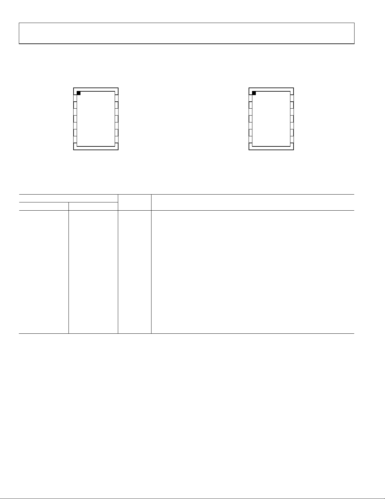
PIN CONFIGURATION AND FUNCTION DESCRIPTIONS
Figure 3. ADP222/ADP224 Pin Configuration
Figure 4. ADP223/ADP225 Pin Configuration
Table 5. Pin Function Descriptions
Pin No.
ADP222/ADP224 ADP223/ADP225 Mnemonic Description
1 1 EN1 Enable Input for the Second Regulator. Drive EN1 high to turn on Regulator 1 and
drive EN1 low to turn off Regulator 1. For automatic startup, connect EN1 to VIN.
2 2 EN2 Enable Input for the First Regulator. Drive EN2 high to turn on Regulator 2 and drive
EN2 low to turn off Regulator 2. For automatic startup, connect EN2 to VIN.
3 3 GND Ground Pin.
N/A1 4 ADJ2 Adjust Pin for VOUT2. A resistor divider from VOUT2 to ADJ2 sets the output
voltage.
4 N/A1 SENSE2 Sense Pin for VOUT2.
5 5 VOUT2 Regulated Output Voltage. Connect an 1 µF or greater output capacitor between
VOUT2 and GND.
6 6 VIN Regulator Input Supply. Bypass VIN to GND with a 1 µF or greater capacitor.
7 7 VOUT1 Regulated Output Voltage. Connect 1 µF or greater output capacitor between
VOUT1 and GND.
N/A1 8 ADJ1 Adjust Pin for VOUT1. A resistor divider from VOUT1 to ADJ1 sets the output
voltage.
8 N/A1 SENSE1 Sense Pin for VOUT1.
EPAD The exposed paddle must be connected to ground.
1
N/A means not applicable.
Rev. B | Page 6 of 24
Data Sheet ADP222/ADP223/ADP224/ADP225
3.20
3.22
3.24
3.26
3.28
3.30
3.32
3.34
3.36
3.38
3.40
–40 –5 25 85 125
V
OUT
(V)
JUNCTION T E M P E R ATURE (° C)
LOAD = 100µA
LOAD = 1mA
LOAD = 10mA
LOAD = 50mA
LOAD = 100mA
LOAD = 300mA
09376-105
2.75
2.76
2.77
2.78
2.79
2.80
2.81
2.82
2.83
2.84
2.85
–40 –5 25 85 125
V
OUT
(V)
JUNCTION T E M P E R ATURE (° C)
09376-106
LOAD = 10µA
LOAD = 100µA
LOAD = 1mA
LOAD = 10mA
LOAD = 100mA
LOAD = 300mA
1.780
1.785
1.790
1.795
1.800
1.805
1.810
1.815
1.820
–40 –5 25 85 125
V
OUT
(V)
JUNCTION T E M P E R ATURE (°C)
LOAD = 10µA
LOAD = 100µA
LOAD = 1mA
LOAD = 10mA
LOAD = 100mA
LOAD = 300mA
09376-107
1.180
1.185
1.190
1.195
1.200
1.205
1.210
1.215
1.220
–40 –5 25 85 125
JUNCTION T E M P E R ATURE (°C)
LOAD = 10µA
LOAD = 100µA
LOAD = 1mA
LOAD = 10mA
LOAD = 100mA
LOAD = 300mA
09376-108
V
OUT
(V)
3.20
3.22
3.24
3.26
3.28
3.30
3.32
3.34
3.36
3.38
3.40
0.01 0.1 1 10 100 1000
V
OUT
(V)
I
LOAD
(mA)
09376-109
2.75
2.76
2.77
2.78
2.79
2.80
2.81
2.82
2.83
2.84
2.85
0.01 0.1 1 10 100 1000
I
LOAD
(mA)
09376-110
V
OUT
(V)
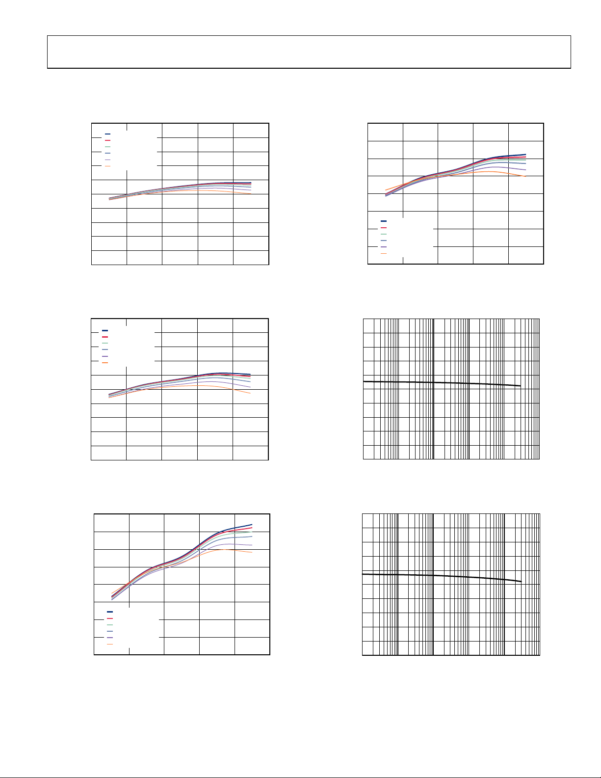
TYPICAL PERFORMANCE CHARACTERISTICS
VIN = 5 V, V
= 3.3 V, V
OUT1
= 2.8 V, I
OUT2
OUT1
= I
= 1 mA, CIN = C
OUT2
= 1 µF, TA = 25°C, unless otherwise noted.
OUT
Figure 5. Output Voltage vs. Junction Temperature, V
ADP222/ADP224
Figure 6. Output Voltage vs. Junction Temperature, V
ADP222/ADP224
OUTx
OUTx
= 3.3 V,
= 2.8 V,
Figure 8. Output Voltage vs. Junction Temperature, V
ADP222/ADP224
Figure 9. Output Voltage vs. Load Current, V
OUTx
= 1.2 V,
OUTx
= 3.3 V, ADP222/ADP224
Figure 7. Output Voltage vs. Junction Temperature, V
ADP222/ADP224
= 1.8 V,
OUTx
Figure 10. Output Voltage vs. Load Current, V
= 2.8 V, ADP222/ADP224
OUTx
Rev. B | Page 7 of 24
ADP222/ADP223/ADP224/ADP225 Data Sheet
1.780
1.785
1.790
1.795
1.800
1.805
1.810
1.815
1.820
0.01 0.1 1 10 100 1000
I
LOAD
(mA)
09376-111
V
OUT
(V)
1.180
1.185
1.190
1.195
1.200
1.205
1.210
1.215
1.220
0.01 0.1 1 10 100 1000
I
LOAD
(mA)
09376-112
V
OUT
(V)
3.20
3.22
3.24
3.26
3.28
3.30
3.32
3.34
3.36
3.38
3.40
3.7 3.9 4.1 4.3 4.5 4.7 4.9 5.1 5.3 5.5
V
OUT
(V)
VIN (V)
LOAD = 10µA
LOAD = 100µA
LOAD = 1mA
LOAD = 10mA
LOAD = 100mA
LOAD = 300mA
09376-113
2.75
2.76
2.77
2.78
2.79
2.80
2.81
2.82
2.83
2.84
2.85
3.7 3.9 4.1 4.3 4.5 4.7 4.9 5.1 5.3 5.5
V
OUT
(V)
V
IN
(V)
LOAD = 10µA
LOAD = 100µA
LOAD = 1mA
LOAD = 10mA
LOAD = 100mA
LOAD = 300mA
09376-114
1.780
1.785
1.790
1.795
1.800
1.805
1.810
1.815
1.820
2.30 2.70 3.10 3.50 3.90 4.30 4.70 5.10 5.50
V
OUT
(V)
VIN (V)
LOAD = 10µA
LOAD = 100µA
LOAD = 1mA
LOAD = 10mA
LOAD = 100mA
LOAD = 300mA
09376-115
1.180
1.185
1.190
1.195
1.200
1.205
1.210
1.215
1.220
2.30 2.70 3.10 3.50 3.90 4.30 4.70 5.10 5.50
V
OUT
(V)
V
IN
(V)
LOAD = 10µA
LOAD = 100µA
LOAD = 1mA
LOAD = 10mA
LOAD = 100mA
LOAD = 300mA
09376-116
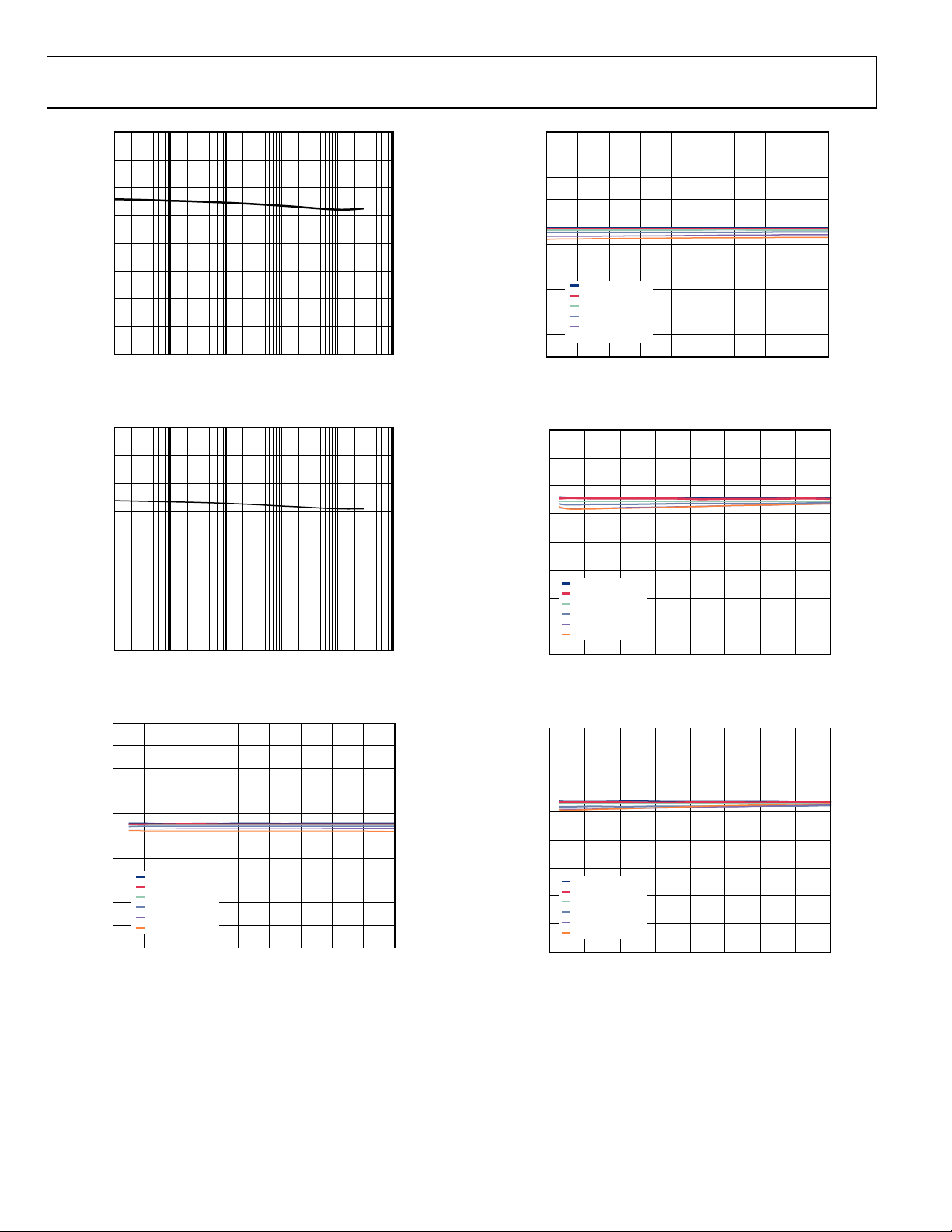
Figure 11. Output Voltage vs. Load Current, V
Figure 12. Output Voltage vs. Load Current, V
= 1.8 V, ADP222/ADP224
OUTx
= 1.2 V, ADP222/ADP224
OUTx
Figure 14. Output Voltage vs. Input Voltage, V
Figure 15. Output Voltage vs. Input Voltage, V
= 2.8 V, ADP222/ADP224
OUTx
= 1.8 V, ADP222/ADP224
OUTx
Figure 13. Output Voltage vs. Input Voltage, V
= 3.3 V, ADP222/ADP224
OUTx
Figure 16. Output Voltage vs. Input Voltage, V
Rev. B | Page 8 of 24
= 1.2 V, ADP222/ADP224
OUTx
 Loading...