Step-Down DC-to-DC Regulator
ADP2164
Rev. A
Information furnished by Analog Devices is believed to be accurate and reliable. However, no
Trademarks and registered trademarks are the property of their respective owners.
Fax: 781.461.3113 ©2011–2021 Analog Devices, Inc. All rights reserved.
09944-001
ADP2164
PGOOD
EN
C
OUT
C1
R2
R
T
C
IN
V
OUT
V
IN
SYNC
TRK
RT
SW
FB
PGND
GND
VIN
L
R1
PVIN
100
95
90
85
80
75
70
65
60
55
50
0 0.5 1.0 1.5 2.0 2.5 3.0 3.5 4.0
OUTPUT CURRE NT (A)
EFFICIENCY (%)
09944-002
VIN = 5V
f
S
= 600kHz
V
OUT
= 1.2V
V
OUT
= 3.3V
Data Sheet
FEATURES
4 A continuous output current
43 mΩ and 29 mΩ integrated FET
±1.5% output accuracy
Input voltage range: 2.7 V to 6.5 V
Output voltage: 0.6 V to V
Switching frequency
Fixed frequency: 600 kHz or 1.2 MHz
Adjustable frequency: 500 kHz to 1.4 MHz
Synchronizable from 500 kHz to 1.4 MHz
Selectable synchronize phase shift: 0° or 180°
Current mode architecture
Precision enable input
Power-good output
Voltage tracking input
Integrated soft start
Internal compensation
Starts up into a precharged output
UVLO, OVP, OCP, and thermal shutdown
Available in 16-lead, 4 mm × 4 mm LFCSP package
Supported by ADIsimPower™ design tool
IN
6.5 V, 4 A, High Efficiency,
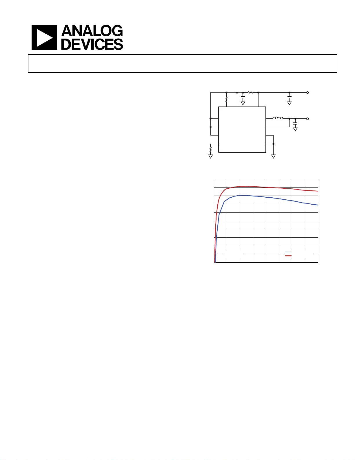
TYPICAL APPLICATIONS CIRCUIT
Figure 1.
APPLICATIONS
Point-of-load conversion
Communications and networking equipment
Industrial and instrumentation
Consumer electronics
GENERAL DESCRIPTION
The ADP2164 is a 4 A, synchronous, step-down dc-to-dc regulator
in a compact 4 mm × 4 mm LFCSP package. The regulator uses a
current mode, constant frequency pulse-width modulation (PWM)
control scheme for excellent stability and transient response.
The input voltage range of the ADP2164 is 2.7 V to 6.5 V. The
output voltage of the ADP2164 is adjustable from 0.6 V to the
input voltage (V
output voltage options: 3.3 V, 2.5 V, 1.8 V, 1.5 V, 1.2 V, and 1.0 V.
responsibility is assumed by Analog Devices for its use, nor for any infringements of patents or other
rights of third parties that may result from its use. Specifications subject to change without noti ce. No
license is granted by implication or otherwise under any patent or patent rights of Analog Devices.
). The ADP2164 is also available in six preset
IN
The ADP2164 integrates a pair of low on-resistance P-channel
and N-channel internal MOSFETs to maximize efficiency and
minimize external component count. The 100% duty cycle
operation allows low dropout voltage at 4 A output current.
The high, 1.2 MHz PWM switching frequency allows the use of
small external components, and the SYNC input enables multiple
ICs to synchronize out of phase to reduce ripple and eliminate
beat frequencies.
Other key features of the ADP2164 include undervoltage lockout
(UVLO), integrated soft start to limit inrush current at startup,
overvoltage protection (OVP), overcurrent protection (OCP),
and thermal shutdown.
One Technology Way, P.O. Box 9106, Norwood, MA 02062-9106, U.S.A.
Tel: 781.329.4700
Figure 2. Efficiency vs. Output Current
www.analog.com

ADP2164 Data Sheet
TABLE OF CONTENTS
Features .............................................................................................. 1
Applications ....................................................................................... 1
Typical Applications Circuit ............................................................ 1
General Description ......................................................................... 1
Revision History ............................................................................... 2
Specifications ..................................................................................... 3
Absolute Maximum Ratings ............................................................ 5
Thermal Resistance ...................................................................... 5
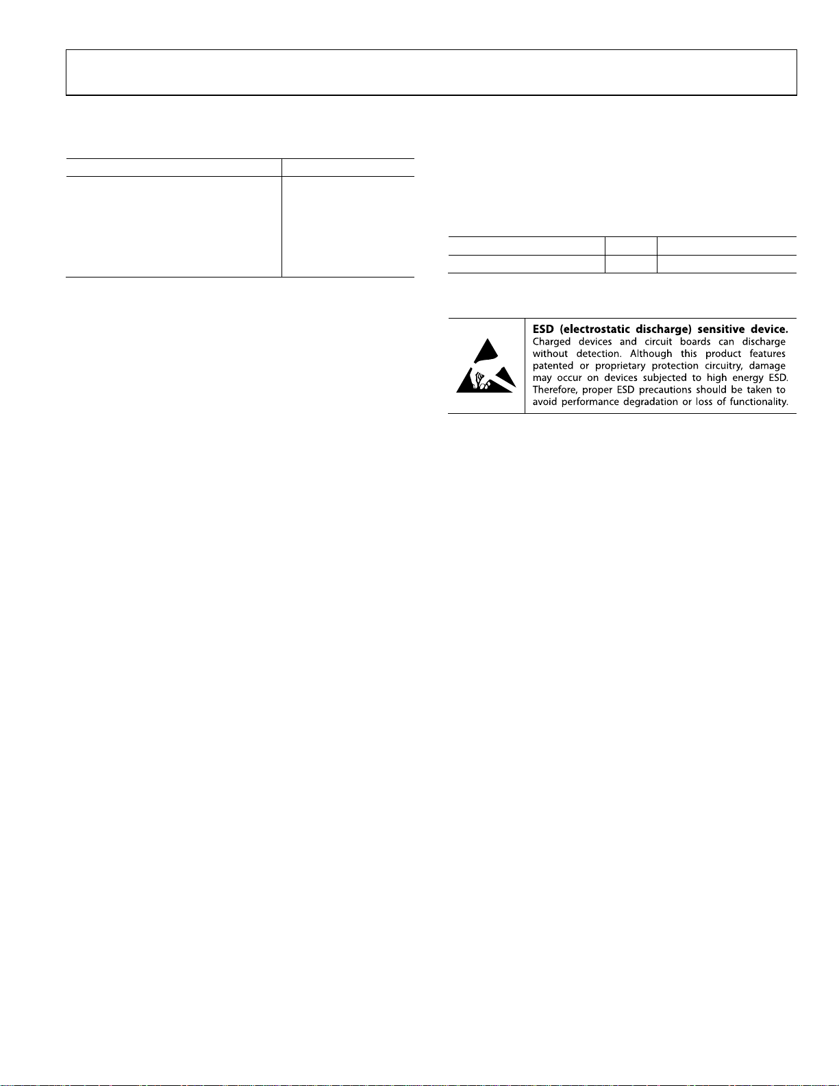
ESD Caution .................................................................................. 5
Pin Configuration and Function Descriptions ............................. 6
Typical Performance Characteristics ............................................. 7
Functional Block Diagram ............................................................ 13
Theory of Operation ...................................................................... 14
Control Scheme .......................................................................... 14
Slope Compensation .................................................................. 14
Precision Enable/Shutdown ...................................................... 14
Integrated Soft Start ................................................................... 14
Oscillator and Synchronization ................................................ 14
Power Good ................................................................................ 15
Current Limit and Short-Circuit Protection ............................ 15
Overvoltage Protection (OVP) ................................................. 15
Undervoltage Lockout (UVLO) ............................................... 15
Thermal Shutdown .................................................................... 15
Applications Information .............................................................. 16
ADIsimPower Design Tool ....................................................... 16
Output Voltage Selection ........................................................... 16
Inductor Selection ...................................................................... 16
Output Capacitor Selection....................................................... 16
Input Capacitor Selection .......................................................... 17
Voltage Tracking ......................................................................... 17
Applications Circuits ...................................................................... 18
Outline Dimensions ....................................................................... 19
Ordering Guide .......................................................................... 19
REVISION HISTORY
6/12—Rev. 0 to Rev. A
Changes to Features Section............................................................ 1
Added ADIsimPower Design Tool Section ................................. 16
12/11—Revision 0: Initial Version
Rev. A | Page 2 of 20

Data Sheet ADP2164
VIN falling
2.4
2.5 V
FB Bias Current
IFB
0.01
0.1
µA
TRK to FB Offset Voltage
TRK = 0 mV to 500 mV
−15 +15
mV
Minimum Pulse Width
100
ns
SPECIFICATIONS
VIN = PVIN = 3.3 V, EN high, SYNC high, TJ = −40°C to +125°C, unless otherwise noted. Typical values are at TJ = 25°C.
Table 1.
Parameter Symbol Test Conditions/Comments Min Typ Max Unit
VIN AND PVIN PINS
VIN Voltage Range VIN 2.7 6.5 V
PVIN Voltage Range PVIN 2.7 6.5 V
Quiescent Current I
Shutdown Current I
VIN Undervoltage Lockout Threshold UVLO VIN rising 2.6 2.7 V
OUTPUT CHARACTERISTICS Specified by the circuit in Figure 42
Load Regulation IO = 0 A to 4 A 0.05 %/A
Line Regulation IO = 2 A 0.05 %/V
FB PIN
FB Regulation Voltage VFB TJ = −40°C to +125°C 0.591 0.6 0.609 V
SW PIN
High-Side On Resistance1 VIN = PVIN = 3.3 V, ISW = 500 mA 35 52 70 mΩ
VIN = PVIN = 5 V, ISW = 500 mA 30 43 55 mΩ
Low-Side On Resistance1 VIN = PVIN = 3.3 V, ISW = 500 mA 24 32 40 mΩ
VIN = PVIN = 5 V, ISW = 500 mA 20 29 35 mΩ
SW Peak Current Limit High-side switch, PVIN = 3.3 V 5 6.2 7.4 A
SW Maximum Duty Cycle Full frequency 100 %
SW Minimum On Time2 Full frequency 100 ns
TRK PIN
TRK Input Voltage Range 0 600 mV
No switching 895 1100 µA
VIN
VIN = PVIN = 6.5 V, EN = GND 9 12 µA
SHDN
TRK Input Bias Current 100 nA
FREQUENCY
Switching Frequency fS RT = VIN 1.08 1.2 1.32 MHz
RT = GND 540 600 660 kHz
RT = 91 kΩ 480 600 720 kHz
Switching Frequency Range 500 1400 kHz
RT Pin Input High Voltage 1.2 V
RT Pin Input Low Voltage 0.45 V
SYNC PIN
Synchronization Range 0.5 1.4 MHz
Minimum Off Time 100 ns
Input High Voltage 1.2 V
Input Low Voltage 0.4 V
PGOOD PIN
Power-Good Range FB rising threshold 105 110 115 %
FB rising hysteresis 2.5 %
FB falling threshold 85 90 95 %
FB falling hysteresis 2.5 %
Power-Good Deglitch Time From FB to PGOOD 16 Clock
Power-Good Leakage Current V
Power-Good Output Low Voltage I
= 5 V 0.1 1 µA
PGOOD
= 1 mA 170 220 mV
PGOOD
cycles
Rev. A | Page 3 of 20

ADP2164 Data Sheet
Parameter Symbol Test Conditions/Comments Min Typ Max Unit
INTEGRATED SOFT START
Soft Start Time All switching frequencies 2048 Clock
cycles
EN PIN
EN Input Rising Threshold 1.12 1.2 1.28 V
EN Input Hysteresis 100 mV
EN Pull-Down Resistor 1 MΩ
THERMAL SHUTDOWN
Thermal Shutdown Threshold TJ increasing 140 °C
Thermal Shutdown Hysteresis 15
1
Pin-to-pin measurements.
2
Guaranteed by design.
°C
Rev. A | Page 4 of 20

Data Sheet ADP2164
FB, SYNC, TRK, RT, EN, PGOOD
−0.3 V to +7 V
θ
ABSOLUTE MAXIMUM RATINGS
Table 2.
Parameter Rating
PVIN, VIN, SW −0.3 V to +7 V
PGND to GND −0.3 V to +0.3 V
Operating Junction Temperature Range −40°C to +125°C
Storage Temperature Range −65°C to +150°C
Soldering Conditions JEDEC J-STD-020
Stresses above those listed under Absolute Maximum Ratings
may cause permanent damage to the device. This is a stress
rating only; functional operation of the device at these or any
other conditions above those indicated in the operational
section of this specification is not implied. Exposure to absolute
maximum rating conditions for extended periods may affect
device reliability.
THERMAL RESISTANCE
θJA is measured using natural convection on a JEDEC 4-layer
board. The exposed pad is soldered to the printed circuit board
with thermal vias.
Table 3. Thermal Resistance
Package Type
16-Lead LFCSP 38.3 °C/W
Unit
JA
ESD CAUTION
Rev. A | Page 5 of 20

ADP2164 Data Sheet
S
D
PIN CONFIGURATION AND FUNCTION DESCRIPTIONS
PGOO
EN
VIN
PVIN
16
15
1
YNC
2
RT
3
TRK
4
FB
NOTES
1. THE EXPOSED PAD SHOULD BE SOLDERED
TO AN EXTERNAL GROUND PLANE UNDER
THE IC FOR THERMAL DISSIPATION.
ADP2164
TOP VIEW
(Not to S cale)
6
5
D
GND
PGN
Figure 3. Pin Configuration
Table 4. Pin Function Descriptions
Pin No. Mnemonic Description
1 SYNC
Synchronization Input. To synchronize the switching frequency to an external clock, connect this pin to an
external clock with a frequency of 500 kHz to 1.4 MHz (see the Oscillator and Synchronization section for
more information).
2 RT
Frequency Setting. To select a switching frequency of 600 kHz, connect this pin to GND; to select a switching
frequency of 1.2 MHz, connect this pin to VIN. To program the frequency from 500 kHz to 1.4 MHz, connect a
resistor from this pin to GND (see the Oscillator and Synchronization section for more information).
3 TRK
Tracking Input. To track a master voltage, connect the TRK pin to a voltage divider from the master voltage. If
the tracking function is not used, connect the TRK pin to VIN. For more information, see the Voltage Tracking
section.
4 FB
Feedback Voltage Sense Input. Connect this pin to a resistor divider from V
connect this pin directly to V
OUT
.
5 GND Analog Ground. Connect to the ground plane.
6, 7, 8 PGND Power Ground. Connect to the ground plane and to the output return side of the output capacitor.
9, 10, 11 SW Switch Node Output. Connect to the output inductor.
12, 13 PVIN
Power Input Pin. Connect this pin to the input power source. Connect a bypass capacitor between this pin
and PGND.
14 VIN
Bias Voltage Input Pin. Connect a bypass capacitor between this pin and GND; connect a small (10 Ω) resistor
between this pin and PVIN.
15 EN
Precision Enable Pin. The external resistor divider can be used to set the turn-on threshold. To enable the
part automatically, connect the EN pin to VIN. This pin has a 1 MΩ pull-down resistor to GND.
16 PGOOD Power-Good Output (Open Drain). Connect this pin to a resistor from any pull-up voltage lower than 6.5 V.
17 (EPAD) Exposed Pad The exposed pad should be soldered to an external ground plane under the IC for thermal dissipation.
13
14
PVIN
12
SW
11
10
SW
9
SW
8
7
GND
PGND
P
09944-003
. For the preset output version,
OUT
Rev. A | Page 6 of 20
 Loading...