

3 MHz, 600 mA, Low Quiescent Current
V
V
V
V
FEATURES
Input voltage range: 2.3 V to 5.5 V
LDO input (VIN2) 1.65 V to 5.5 V
Buck output voltage range: 1.0 V to 3.3 V
LDO output voltage range: 0.8 V to 3.3 V
Buck output current: 600 mA
LDO output current: 300 mA
LDO quiescent current: 22 μA with zero load
Buck quiescent current: 20 μA in PSM mode
Low shutdown current: <0.3 μA
Low LDO dropout 110 mV @ 300 mA load
High LDO PSRR
65 dB @ 10 kHz at V
55 dB @ 100 kHz at V
Low noise LDO: 40 μV rms at V
Initial accuracy: ±1%
Current-limit and thermal overload protection
Power-good indicator
Optional enable sequencing
10-lead 0.75 mm × 3 mm × 3 mm LFCSP package
APPLICATIONS
Mobile phones
Personal media players
Digital camera and audio devices
Portable and battery-powered equipment
GENERAL DESCRIPTION
The ADP2140 includes a high efficiency, low quiescent 600 mA
stepdown dc-to-dc converter and a 300 mA LDO packaged in a
small 10-lead 3 mm × 3 mm LFCSP. The total solution requires
only four tiny external components.
The buck regulator uses a proprietary high speed current-mode,
constant frequency, pulse-width modulation (PWM) control
scheme for excellent stability and transient response. To ensure
the longest battery life in portable applications, the ADP2140 has
a power saving variable frequency mode to reduce switching frequency under light loads.
The LDO is a low quiescent current, low dropout linear regulator
designed to operate in a split supply mode with V
1.65 V. The low input voltage minimum allows the LDO to be
powered from the output of the buck regulator increasing efficiency and reducing power dissipation. The ADP2140 runs from
input voltages of 2.3 V to 5.5 V allowing single Li+/Li− polymer
OUT2
OUT2
= 1.2 V
= 1.2 V
OUT2
= 1.2 V
as low as
IN2
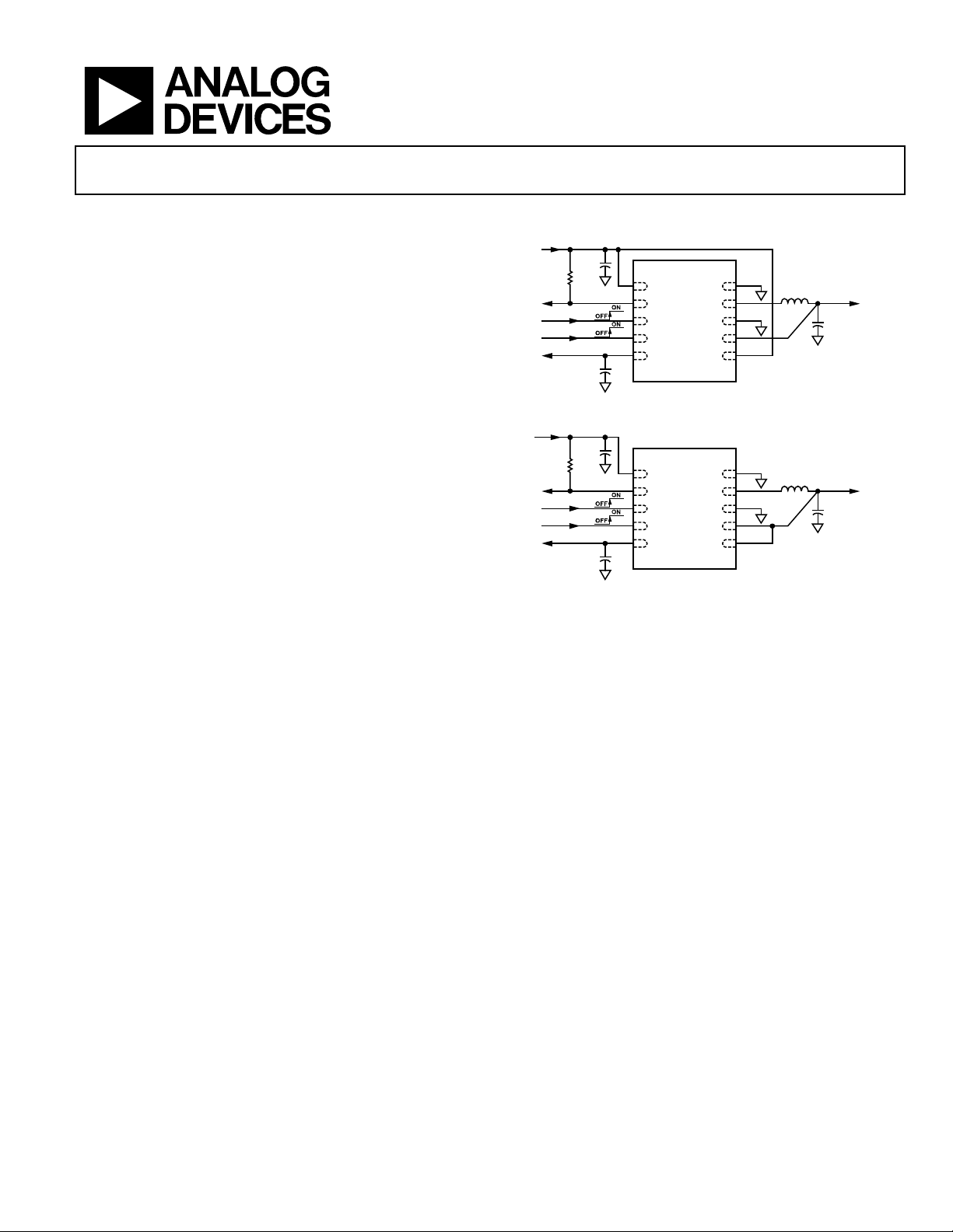
Buck with 300 mA LDO Regulator
ADP2140
TYPICAL APPLICATION CIRCUITS
= 3.6
IN1
+
C
IN
10µF
100kΩ
PG
EN1
EN2 FB
V
= 1.8V
OUT2
+
C
OUT2
1µF
Figure 1. ADP2140 with LDO Connected to V
= 3.3
IN1
+
C
IN
10µF
100kΩ
PG
EN1
EN2 FB
V
= 1.2V
OUT2
+
C
OUT2
1µF
Figure 2. ADP2140 with LDO Connected to Buck Output
cell, multiple alkaline/NiMH cell, PCMCIA, and other standard
power sources.
ADP2140 includes a power-good pin, soft start, and internal
compensation. Numerous power sequencing options are userselectable through two enable inputs. In autosequencing mode,
the highest voltage output enables on the rising edge of EN1.
During logic controlled shutdown, the input disconnects from
the output and draws less than 300 nA from the input source.
Other key features include: undervoltage lockout to prevent deep
battery discharge, soft start to prevent input current overshoot
at startup, and both short-circuit protection and thermal overload
protection circuits to prevent damage in adverse conditions.
When the ADP2140 is used with two 0603 capacitors, one 0402
capacitor, one 0402 resistor, and one 0805 chip inductor, the total
solution size is approximately 90 mm
print solution to meet a variety of portable applications.
10
9
8
7
6
10
9
8
7
6
ADP2140
VIN1 PGND
PG SW
EN1 AGND
EN2
VOUT2
VIN2
ADP2140
VIN1 PGND
PG SW
EN1 AGND
EN2
VOUT2
VIN2
1
2
3
4
5
1
2
3
4
5
2
resulting in the smallest foot-
1µH
1µH
V
= 1.2V
OUT
+
C
OUT
10µF
IN1
V
= 1.8V
OUT
+
C
OUT
10µF
07932-001
07932-002
Rev. 0
Information furnished by Analog Devices is believed to be accurate and reliable. However, no
responsibility is assumed by Analog Devices for its use, nor for any infringements of patents or other
rights of third parties that may result from its use. Specifications subject to change without notice. No
license is granted by implication or otherwise under any patent or patent rights of Analog Devices.
Trademarks and registered trademarks are the property of their respective owners.
One Technology Way, P.O. Box 9106, Norwood, MA 02062-9106, U.S.A.
Tel: 781.329.4700 www.analog.com
Fax: 781.461.3113 ©2010 Analog Devices, Inc. All rights reserved.

ADP2140
TABLE OF CONTENTS
Features .............................................................................................. 1
Applications ....................................................................................... 1
General Description ......................................................................... 1
Typical Application Circuits ............................................................ 1
Revision History ............................................................................... 2
Specifications ..................................................................................... 3
Recommended Specifications: Capacitors and Inductor ........ 4
Absolute Maximum Ratings ............................................................ 5
Thermal Data ................................................................................ 5
Thermal Resistance ...................................................................... 5
ESD Caution .................................................................................. 5
Pin Configuration and Function Descriptions ............................. 6
Typical Performance Characteristics ............................................. 7
Buck Output .................................................................................. 7
LDO Output ................................................................................ 14
Theory of Operation ...................................................................... 19
Buck Section ................................................................................ 19
Control Scheme .......................................................................... 19
PWM Operation ......................................................................... 19
PSM Operation ........................................................................... 19
Pulse Skipping Threshold .......................................................... 19
Selected Features ............................................................................. 20
Short-Circuit Protection ............................................................ 20
Undervoltage Lockout ............................................................... 20
Thermal Protection .................................................................... 20
Soft Start ...................................................................................... 20
Current Limit .............................................................................. 20
Power-Good Pin ......................................................................... 20
LDO Section ............................................................................... 20
Applications Information .............................................................. 21
Power Sequencing ...................................................................... 21
Power-Good Function ............................................................... 24
External Component Selection ................................................ 24
Selecting the Inductor ................................................................ 24
Output Capacitor ........................................................................ 24
Input Capacitor ........................................................................... 24
Efficiency ..................................................................................... 25
Recommended Buck External Components .......................... 25
LDO Capacitor Selection .......................................................... 26
LDO as a Postregulator to Reduce Buck Output Noise ........ 26
Thermal Considerations ................................................................ 28
PCB Layout Considerations ...................................................... 29
Outline Dimensions ....................................................................... 30
Ordering Guide .......................................................................... 30
REVISION HISTORY
6/10—Revision 0: Initial Version
Rev. 0 | Page 2 of 32

ADP2140
SPECIFICATIONS
V
= 3.6 V, V
IN1
C
= 10 µF, C
OUT
specifications, unless otherwise noted.
Table 1.
Parameter Symbol Test Conditions/Comments Min Typ Max Unit
BUCK SECTION
Input Voltage Range V
Buck Output Accuracy V
V
Transient Load Regulation V
Load = 50 mA to 250 mA, rise/fall time = 200 ns 75 mV
Load = 200 mA to 600 mA, rise/fall time = 200 ns 75 mV
Transient Line Regulation V
V
V
V
PWM To PSM Threshold V
Output Current I
Current Limit I
Switch On Resistance
PFET R
NFET R
Switch Leakage Current I
Quiescent Current IQ No load, device not switching 20 30 A
Minimum On Time ON-TIME
Oscillator Frequency FREQ 2.55 3.0 3.15 MHz
Frequency Foldback Threshold V
Start-Up Time1 t
Soft Start Time2 SS
LDO SECTION
Input Voltage Range V
LDO Output Accuracy V
1 mA < I
Line Regulation
Load Regulation3
Dropout Voltage4 V
I
Ground Current I
I
I
Power Supply Rejection Ratio PSRR V
PSRR on V
100 kHz, V
100 kHz, V
100 kHz, V
IN2
= V
OUT2
+ 0.3 V or 1.65 V, whichever is greater; 5 V EN1 = EN2 = V
OUT2
= 1 µF, L
= 1 H; TJ = −40°C to +125°C for minimum/maximum specifications, and TA = 25°C for typical
OUT
2.3 5.5 V
IN1
I
OUT
TR-LOAD
Line transient = 4 V to 5 V, 4 s rise time
TR-LINE
600 mA
OUT
V
LIM
V
PFET
V
NFET
EN1 = GND, VIN1 = 5.5 V, and SW = 0 V −1 A
LEAK-SW
Output voltage where fSW ≤ 50% of nominal frequency 50 %
FOLD
START-UP
V
TIME
1.65 5.5 V
IN2
I
OUT2
OUT
IN1
V
V
OUT
OUT
OUT
OUT
IN1
IN1
IN1
IN1
70 ns
MIN
OUT
OUT
OUT2
1 mA < I
= 25°C
V
/V
OUT2
V
/I
OUT2
DROPOUT
No load, buck disabled 22 35 A
AGND
10 kHz, V
IN2
V
IN2
IN2
I
OUT2
OUT2
I
OUT2
OUT2
OUT2
OUT2
IN2
; I
IN1
= 200 mA, I
OUT
= 10 mA, CIN = 10 F,
OUT2
= 10 mA −1.5 +1.5 %
= 2.3 V or (V
+ 0.5 V) to 5.5 V, I
OUT
= 1 mA to 600 mA −2.5 +2.5 %
OUT
= 1.8 V
= 1.0 V 40 mV
= 1.8 V 25 mV
= 3.3 V 25 mV
= 2.3 V or (V
= 2.3 V or (V
+ 0.5 V) to 5.5 V 100 mA
OUT
+ 0.5 V) to 5.5 V 1100 1300 mA
OUT
= 2.3 V to 5.5 V 250 mΩ
= 2.3 V to 5.5 V 250 mΩ
= 1.8 V, 600 mA load 70 µs
= 1.8 V, 600 mA load 150 s
= 10 mA, TJ = 25°C −1 +1 %
−1.5 +1.5 %
= (V
< 300 mA, V
OUT2
< 300 mA, V
OUT2
+ 0.3 V) to 5.5 V, I
OUT2
IN2
IN2
= (V
= (V
+ 0.3 V) to 5.5 V, TJ
OUT2
+ 0.3 V) to 5.5 V −3 +3 %
OUT2
= 10 mA −0.05 +0.05 %/V
OUT2
= 1 mA to 300 mA 0.001 0.005 %/mA
= 10 mA, V
= 300 mA, V
= 1.8 V 4 7 mV
OUT2
= 1.8 V 110 200 mV
OUT2
= 10 mA 65 90 A
= 300 mA 150 220 A
= V
OUT2
OUT2
+ 1 V, V
OUT2
OUT2
OUT2
= 5 V, I
IN1
= 10 mA
OUT2
= 1.2 V, 1.8 V, 3.3 V 65 dB
= 3.3 V 53 dB
= 1.8 V 54 dB
= 1.2 V 55 dB
Rev. 0 | Page 3 of 32
ADP2140
Parameter Symbol Test Conditions/Comments Min Typ Max Unit
Output Noise OUT
10 Hz to 100 kHz, V
10 Hz to 100 kHz, V
10 Hz to 100 kHz, V
10 Hz to 100 kHz, V
10 Hz to 100 kHz, V
Current Limit I
Input Leakage Current I
Start-Up Time1 t
Soft Start Time2 SS
ADDITIONAL FUNCTIONS
Undervoltage Lockout UVLO
Input Voltage Rising UVLO
Input Voltage Falling UVLO
EN Input
EN1, EN2 Input Logic High VIH 2.3 V ≤ V
EN1, EN2 Input Logic Low VIL 2.3 V ≤ V
EN1, EN2 Input Leakage I
EN1, EN2 = V
Shutdown Current I
Thermal Shutdown
Threshold TSSD T
Hysteresis TS
Power Good
Rising Threshold PG
Falling Threshold PG
Power-Good Hysteresis PG
Output Low VOL I
Leakage Current IOH Power-good pin pull-up voltage = 5.5 V 1 A
Buck to LDO Delay t
Power-Good Delay t
1
Start-up time is defined as the time between the rising edge of ENx to V
2
Soft start time is defined as the time between V
3
Based on an endpoint calculation using 1 mA and 300 mA loads.
4
Dropout voltage is defined as the input-to-output voltage differential when the input voltage is set to the nominal output voltage. This applies only for output
voltages above 2.3 V.
V
NOISE
T
LIM
EN2 = GND, V
LEAK-LDO
V
START-UP
V
TIME
2.23 2.3 V
RISE
2.05 2.16 V
FAL L
EN1, EN2 = V
EN-LKG
V
SHUT
20
SD-HYS
92 %V
RISE
86 %V
FAL L
6 %V
HYS
PWM mode only 5 ms
DELAY
PWM mode only 5 ms
RESET
being at 10% to V
OUTx
= V
= 5 V, I
IN2
IN1
= 25°C 360 500 760 mA
J
= 3.3 V, 300 mA load 70 µs
OUT2
= 3.3 V, 300 mA load 130 s
OUT2
≤ 5.5 V 1.0 V
IN1
≤ 5.5 V 0.27 V
IN1
= 5.5 V, EN1, EN2 = GND, TJ = −40°C to +85°C 0.3 1.2 A
IN1
rising 150
J
= 4 mA 0.2 V
SINK
OUTx
being at 90% of the V
OUTx
= 10 mA
OUT2
= 0.8 V 29 µV rms
OUT2
= 1.2 V 40 µV rms
OUT2
= 1.8 V 50 µV rms
OUT2
= 2.5 V 66 µV rms
OUT2
= 3.3 V 88 µV rms
OUT2
= 5.5 V and V
IN2
or GND 0.05 µA
IN1
or GND 1 µA
IN1
being at 10% of the V
= 0 V 1 A
OUT2
nominal value.
OUTx
nominal value.
OUTx
°C
°C
OUT
OUT
OUT
RECOMMENDED SPECIFICATIONS: CAPACITORS AND INDUCTOR
Table 2.
Parameter Symbol Test Conditions/Comments Min Typ Max Unit
MINIMUM INPUT AND OUTPUT CAPACITANCE1
Buck C
LDO C
MIN
MIN
CAPACITOR ESR
Buck R
LDO R
MINIMUM INDUCTOR IND
1
The minimum input and output capacitance should be greater than 0.70 F over the full range of operating conditions. The full range of operating conditions in the
application must be considered during device selection to ensure that the minimum capacitance specification is met. X7R- and X5R-type capacitors are recommended,
Y5V and Z5U capacitors are not recommended for use with any LDO.
ESR
ESR
MIN
Rev. 0 | Page 4 of 32
TA = −40°C to +125°C
TA = −40°C to +125°C
7.5 10 µF
0.7 1.0 µF
Ω
0.001 0.01 Ω
0.001 1 Ω
0.7 1 H
ADP2140
ABSOLUTE MAXIMUM RATINGS
Table 3.
Parameter Rating
VIN1, VIN2 to PGND, AGND −0.3 V to +6.5 V
VOUT2 to PGND, AGND −0.3 V to V
SW to PGND, AGND −0.3 V to V
IN2
IN1
FB to PGND, AGND −0.3 V to +6.5 V
PG to PGND, AGND −0.3 V to +6.5 V
EN1, EN2 to PGND, AGND −0.3 V to +6.5 V
Storage Temperature Range −65°C to +150°C
Operating Ambient Temperature Range −40°C to +85°C
Operating Junction Temperature Range −40°C to +125°C
Soldering Conditions JEDEC J-STD-020
Stresses above those listed under Absolute Maximum Ratings
may cause permanent damage to the device. This is a stress
rating only; functional operation of the device at these or any
other conditions above those indicated in the operational
section of this specification is not implied. Exposure to absolute
maximum rating conditions for extended periods may affect
device reliability.
THERMAL DATA
Absolute maximum ratings apply individually only, not in com-
bination. The ADP2140 can be damaged when the junction
temperature limits are exceeded. Monitoring ambient temperature
does not guarantee that T
limits. In applications with high power dissipation and poor
thermal resistance, the maximum ambient temperature may
need to be derated.
In applications with moderate power dissipation and low
is within the specified temperature
J
Junction-to-ambient thermal resistance (θ
based on modeling and calculation using a 4-layer board. The
junction-to-ambient thermal resistance is highly dependent on
the application and board layout. In applications where high
maximum power dissipation exists, close attention to thermal
board design is required. The value of θ
on PCB material, layout, and environmental conditions. The
specified values of θ
board. Refer to JESD 51-7 for detailed information on the board
construction.
For more information, see
and Manufacturing Guide for the Lead Frame Chip Scale Package
(LFCSP).
Ψ
is the junction-to-board thermal characterization parameter
JB
with units of °C/W. Ψ
calculation using a 4-layer board. The JESD51-12, Guidelines for
Reporting and Using Package Thermal Information, states that
thermal characterization parameters are not the same as thermal
resistances. Ψ
multiple thermal paths rather than a single path, as in thermal
resistance, θ
from the top of the package as well as radiation from the package,
factors that make Ψ
Maximum junction temperature (T
board temperature (T
formula
T
= TB + (PD × ΨJB)
J
Refer to JESD51-8 and JESD51-12 for more detailed
information about Ψ
printed circuit board (PCB) thermal resistance, the maximum
ambient temperature can exceed the maximum limit as long as
the junction temperature is within specification limits. The
junction temperature (T
ambient temperature (T
(P
), and the junction-to-ambient thermal resistance of the
D
package (θ
).
JA
Maximum junction temperature (T
ambient temperature (T
) of the device is dependent on the
J
), the power dissipation of the device
A
) is calculated from the
J
) and power dissipation (PD) using the
A
formula
T
= TA + (PD × θJA)
J
THERMAL RESISTANCE
θJA and ΨJB are specified for the worst-case conditions, that is, a
device soldered in a circuit board for surface-mount packages.
Table 4. Thermal Resistance
Package Type θJA ΨJB Unit
10-Lead 3 mm × 3 mm LFCSP 35.3 16.9 °C/W
ESD CAUTION
are based on a 4-layer, 4 in. × 3 in. circuit
JA
AN-772 Application Note, A Design
of the package is based on modeling and
JB
measures the component power flowing through
JB
. Therefore, ΨJB thermal paths include convection
JB
more useful in real-world applications.
JB
J
) and power dissipation (PD) using the
B
.
JB
) of the package is
JA
may vary, depending
JA
) is calculated from the
Rev. 0 | Page 5 of 32
ADP2140
PIN CONFIGURATION AND FUNCTION DESCRIPTIONS
PGND
AGND
NOTES
1. THE EXPOSED PAD ON THE BOTTOM OF T HE LFCSP PACKAGE E NHANCES
THERMAL PERF ORMANCE AND IS EL ECTRICALLY CONNECTED TO G ROUND
INSIDE THE PACKAGE. IT IS RECOMMENDE D T HAT THE EXPO SED PAD BE
CONNECTED TO THE GROUND PL ANE ON THE CIRCUIT BOARD.
SW
VIN2
FB
1
2
ADP2140
TOP VIEW
3
(Not to S cale)
4
5
VIN1
10
PG
9
EN1
8
EN2
7
VOUT2
6
Figure 3. Pin Configuration
Table 5. Pin Function Descriptions
Pin Mnemonic Description
1 PGND Power Ground.
2 SW Connection from Power MOSFETs to Inductor.
3 AGND Analog Ground.
4 FB Feedback from Buck Output.
5 VIN2 LDO Input Voltage.
6 VOUT2 LDO Output Voltage.
7 EN2 Logic 1 to Enable LDO or No Connect for Autosequencing.
8 EN1
Logic 1 to Enable Buck or Initiate Sequencing. This is a dual function pin and the state of EN2 determines
which function is operational.
9 PG
Power Good. Open-drain output. PG is held low until both output voltages (which includes the external
inductor and capacitor sensed by the FB pin) rise above 92% of nominal value. PG is held high until both
outputs fall below 85% of nominal value.
10 VIN1 Analog Power Input.
EP
Exposed Pad. The exposed pad on the bottom of the LFCSP package enhances thermal performance and is
electrically connected to ground inside the package. It is recommended that the exposed pad be connected
to the ground plane on the circuit board.
07932-003
Rev. 0 | Page 6 of 32
ADP2140
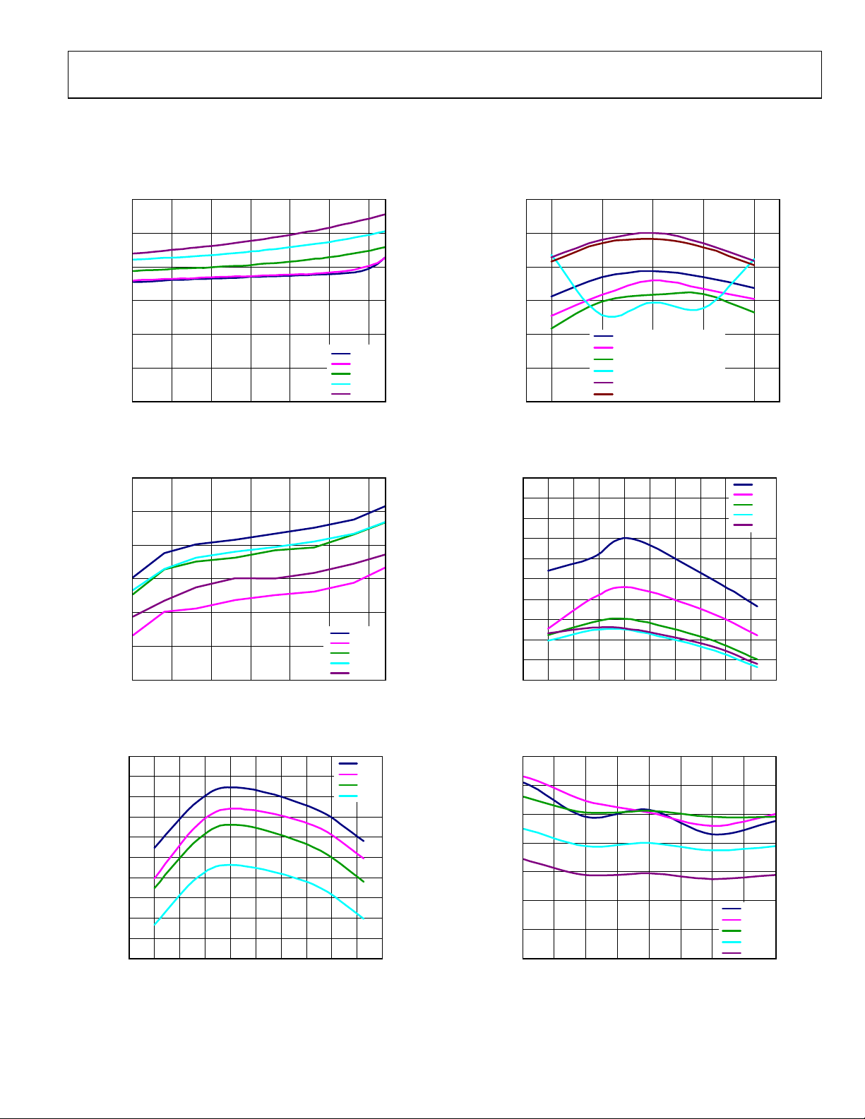
TYPICAL PERFORMANCE CHARACTERISTICS
BUCK OUTPUT
V
= 4 V, V
IN1
= 1.8 V, I
OUT
30
= 10 mA, CIN = C
OUT
= 10 µF, TA = 25°C, unless otherwise noted.
OUT
1.82
25
20
15
10
QUIESCENT CURRENT (µA)
5
0
2.3 2.8 3.3 3.8 4.3 4.8 5.3
INPUT VOLTAGE ( V)
–40°C
–5°C
+25°C
+85°C
+125°C
07932-004
Figure 4. Quiescent Supply Current vs. Input Voltage, Different Temperatures
3.1
3.0
2.9
2.8
2.7
FREQUENCY (MHz )
+25°C
2.6
2.5
2.3 2.8 3.3 3.8 4.3 4.8 5.3
INPUT VOLTAGE ( V)
–40°C
–5°C
+85°C
+125°C
07932-005
Figure 5. Switching Frequency vs. Input Voltage, Different Temperatures
3.10
3.05
3.00
2.95
2.90
2.85
2.80
FREQUENCY (MHz )
2.75
2.70
2.65
2.60
–60 –40 –20 0 20 40 60 80 100 120 140
TEMPERATURE ( °C)
5.5V
4.6V
3.1V
2.3V
07932-006
Figure 6. Switching Frequency vs. Temperature, Different Input Voltages
1.81
1.80
1.79
1.78
OUTPUT VOLTAGE (V)
1.77
1.76
–40 1258525–5
Figure 7. Output Voltage vs. Temperature, V
LOAD CURRENT = 1mA
LOAD CURRENT = 10mA
LOAD CURRENT = 50mA
LOAD CURRENT = 100mA
LOAD CURRENT = 300mA
LOAD CURRENT = 600mA
JUNCTION TEM PERATURE (°C)
= 2.3 V, Different Loads
IN1
1200
1150
1100
1050
1000
950
900
850
CURRENT LIMI T (mA)
800
750
700
–60 –40 –20 0 20 40 60 80 100 120 140
JUNCTION TEMPERATURE (° C)
2.3V
3.0V
4.0V
5.0V
5.5V
Figure 8. Current Limit vs. Temperature, Different Input Voltages
140
120
100
80
60
CURRENT (mA)
40
20
0
3.50 5.505.255.004.754.504.254.003.75
INPUT VOLTAGE (V)
–40°C
–5°C
+25°C
+85°C
+125°C
Figure 9. PSM to PWM Mode Transition vs. Input Voltage, Different
Temperatures
07932-007
07932-008
07932-009
Rev. 0 | Page 7 of 32
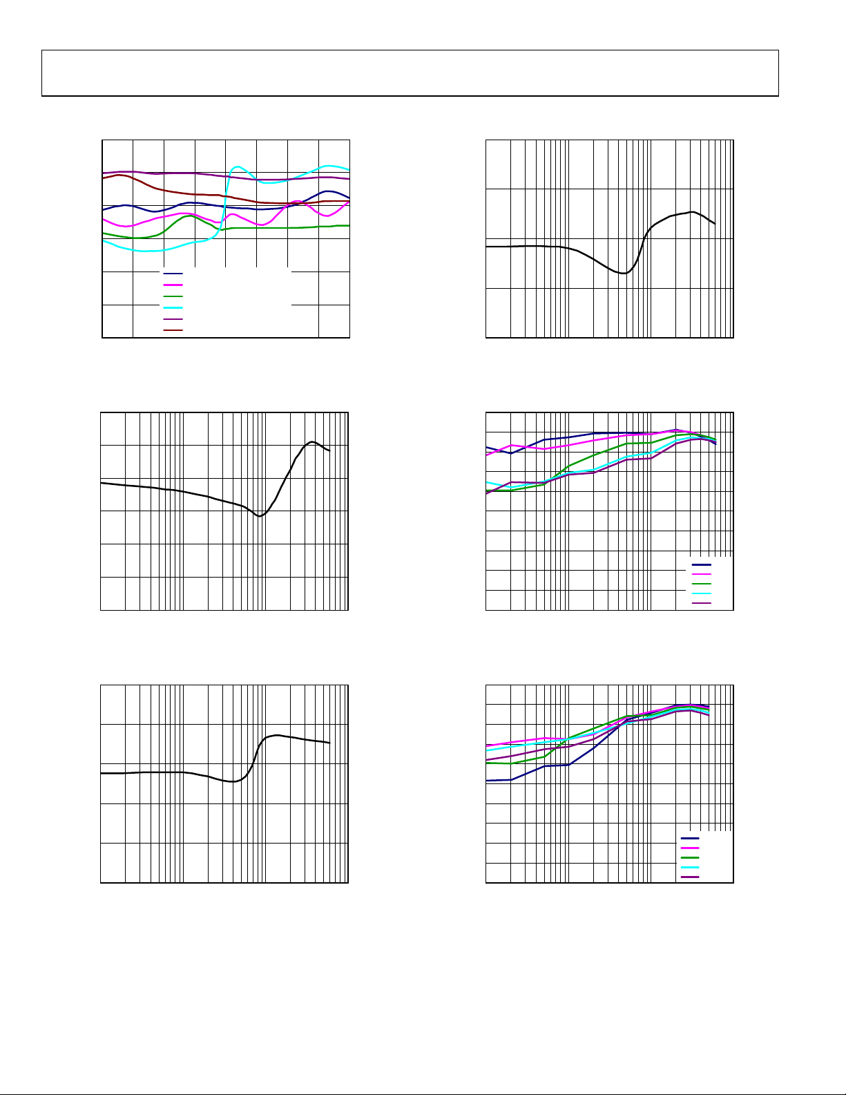
ADP2140
V
= 4 V, V
IN1
OUT
1.82
1.81
1.80
= 1.8 V, I
= 10 mA, CIN = C
OUT
= 10 µF, TA = 25°C, unless otherwise noted.
OUT
3.350
3.325
1.79
1.78
OUTPUT VOLTAGE (V)
1.77
1.76
2.3 5.55.14.74.33.93.53.12.7
Figure 10. Line Regulation, V
LOAD CURRENT = 1mA
LOAD CURRENT = 10mA
LOAD CURRENT = 50mA
LOAD CURRENT = 100mA
LOAD CURRENT = 300mA
LOAD CURRENT = 600mA
INPUT VOLTAG E ( V)
= 1.8 V, Different Loads
OUT
1.82
1.81
1.80
1.79
1.78
OUTPUT VOLTAGE (V)
1.77
1.76
1 10 100 1000
Figure 11. Load Regulation, V
LOAD CURRENT (mA)
= 1.8 V, V
OUT
IN1
1.22
1.21
1.20
1.19
OUTPUT VOLTAGE (V)
1.18
1.17
1 10 100 1000
Figure 12. Load Regulation, V
LOAD CURRENT (mA)
= 1.2 V, V
OUT
IN1
07932-010
07932-011
= 2.3 V
07932-012
= 2.3 V
3.300
OUTPUT VOLTAGE (V)
3.275
3.250
1 10 100 1000
LOAD CURRENT (mA)
Figure 13. Load Regulation, V
100
90
80
70
60
50
40
EFFICIENCY (%)
30
20
10
0
1 10 100 1000
LOAD CURRENT (mA)
Figure 14. Efficiency vs. Load Current, V
100
90
80
70
60
50
40
EFFICIENCY (%)
30
20
10
0
1 10 100 1000
LOAD CURRENT (mA)
Figure 15. Efficiency vs. Load Current, V
= 3.3 V
OUT
2.5V
3.0V
4.0V
5.0V
5.5V
= 1.8 V, Different Input Voltages
OUT
–40°C
–5°C
+25°C
+85°C
+125°C
= 1.8 V, Different Temperatures
OUT
07932-013
07932-014
07932-015
Rev. 0 | Page 8 of 32
ADP2140
V
= 4 V, V
IN1
100
90
80
70
60
50
40
EFFICIENCY (%)
30
20
10
Figure 16. Efficiency vs. Load Current, V
100
90
80
70
60
50
40
EFFICIENCY (%)
30
20
10
Figure 17. Efficiency vs. Load Current, V
= 1.8 V, I
OUT
0
1 10 100 1000
= 10 mA, CIN = C
OUT
LOAD CURRENT (mA)
= 1.2 V, Different Input Voltages
OUT
= 10 μF, TA = 25°C, unless otherwise noted.
OUT
2.5V
3.0V
4.0V
5.0V
5.5V
–40°C
–5°C
+25°C
+85°C
0
1 10 100 1000
LOAD CURRENT (mA)
= 1.2 V, Different Temperatures
OUT
+125°C
100
90
80
70
60
50
40
EFFICIENCY (%)
30
20
10
0
1 10 100 1000
07932-016
Figure 19. Efficiency vs. Load Current, V
LOAD CURRENT (mA)
= 3.3 V, Different Temperatures
OUT
–40°C
–5°C
+25°C
+85°C
+125°C
07932-019
100
90
80
70
60
50
40
EFFICIENCY (%)
30
20
10
0
1 10 100 1000
07932-017
Figure 20. Efficiency vs. Load Current, V
LOAD CURRENT (mA)
= 3.3 V, Different Input Voltages
OUT
4.0V
5.0V
5.5V
07932-018
T
2
1
3
CH1 1.00V CH2 50.0mV M20.0µs A CH1 4.68V
Figure 18. Line Transient, V
INPUT VOLTAGE
OUTPUT VOLTAGE
SWITCH NO DE
T 11.60%CH3 5.00V
= 1.8 V, Power Save Mode, 50 mA,
OUT
= 4 V to 5 V, 4 μs Rise Time
V
IN1
07932-020
Rev. 0 | Page 9 of 32
T
2
1
3
CH1 1.00V CH2 20.0mV M20. 0µ s A CH1 4.68V
Figure 21. Line Transient, V
INPUT VOLTAGE
OUTPUT VOLTAGE
SWITCH NO DE
T 11.60%CH3 5.00V
= 1.8 V, PWM Mode, 600 mA, V
OUT
4 μs Rise Time
= 4 V to 5 V,
IN1
07932-021
ADP2140
V
= 4 V, V
IN1
OUT
= 1.8 V, I
= 10 mA, CIN = C
OUT
= 10 µF, TA = 25°C, unless otherwise noted.
OUT
T
2
1
3
CH1 1.00V CH2 50.0mV M20.0µs A CH1 4.68V
Figure 22. Line Transient, V
INPUT VOLTAGE
OUTPUT VOLTAGE
SWITCH NO DE
T 11.60%CH3 5.00V
= 1.2 V, PSM Mode, 50 mA, V
OUT
4 s Rise Time
T
2
1
INPUT VOLTAGE
OUTPUT VOLTAGE
SWITCH NO DE
= 4 V to 5 V,
IN1
T
2
1
3
CH1 1.00V CH2 20.0mV M20. 0µ s A CH1 4.68V
07932-022
Figure 25. Line Transient, V
INPUT VOLTAGE
OUTPUT VOLTAGE
SWITCH NO DE
T 11.60%CH3 5.00V
= 3.3 V, PWM Mode, 600 mA, V
OUT
07932-025
= 4 V to 5 V,
IN1
4 s Rise Time
T
3
1
2
SWITCH NO DE
LOAD CURRENT
OUTPUT VOLTAGE
3
CH1 1.00V CH2 20.0mV M20. 0µ s A CH1 4.32V
Figure 23. Line Transient, V
T
2
1
3
CH1 1.00V CH2 50.0mV M20. 0µ s A CH1 4.68V
Figure 24. Line Transient, V
T 10.80%CH3 5.00V
= 1.2 V, PWM Mode, 600 mA, V
OUT
4 s Rise Time
INPUT VOLTAGE
OUTPUT VOLTAGE
SWITCH NO DE
T 11.60%CH3 5.00V
= 3.3 V, PSM Mode, 50 mA, V
OUT
4 s Rise Time
= 4 V to 5 V,
IN1
= 4 V to 5 V,
IN1
CH1 200mA CH2 50.0mV M20.0µs A CH1 288mA
07932-023
Figure 26. Load Transient, V
OUT
T 10.40%CH3 5.00V
07932-026
= 1.8 V, 200 mA to 600 mA, Load Current Rise
Time = 200 ns
T
3
1
2
CH1 100mA CH2 50.0mV M20.0µs A CH1 136mA
07932-024
Figure 27. Load Transient, V
SWITCH NO DE
LOAD OUTPUT
OUTPUT VOLTAGE
T 10.40%CH3 5.00V
= 1.8 V, 50 mA to 250 mA, Load Current Rise
OUT
07932-027
Time = 200 ns
Rev. 0 | Page 10 of 32

ADP2140
V
= 4 V, V
IN1
= 1.8 V, I
OUT
= 10 mA, CIN = C
OUT
= 10 µF, TA = 25°C, unless otherwise noted.
OUT
T
3
LOAD CURRENT
1
2
CH1 50.0mA CH2 50.0mV M20.0µs A CH1 51.0mA
Figure 28. Load Transient, V
SWITCH NO DE
OUTPUT VOLTAGE
T 10.40%CH3 5.00V
= 1.8 V,10 mA to 110 mA, Load Current Rise
OUT
Time = 200 ns
T
3
LOAD CURRENT
1
SWITCH NO DE
T
3
LOAD CURRENT
1
2
CH1 50.0mA CH2 100.0mV M20.0µs A CH1 50. 0 mA
07932-028
Figure 31. Load Transient, V
SWITCH NO DE
OUTPUT VO LTAGE
T 10.40%CH3 5.00V
= 3.3 V,10 mA to 110 mA, Load Current Rise
OUT
07932-031
Time = 200 ns
T
SWITCH NO DE
3
1
LOAD CURRENT
2
CH1 200mA CH2 100.0mV M20.0µs A CH1 292mA
Figure 29. Load Transient, V
T
3
LOAD CURRENT
1
2
CH1 100mA CH2 100.0mV M20.0µs A CH1 80.0mA
Figure 30. Load Transient, V
OUTPUT VOLTAGE
T 10.40%CH3 5.00V
= 3.3 V, 200 mA to 600 mA, Load Current Rise
OUT
Time = 200 ns
SWITCH NO DE
OUTPUT VOLTAGE
T 10.40%CH3 5.00V
= 3.3 V, 50 mA to 250 mA, Load Current Rise
OUT
Time = 200 ns
2
CH1 200.0mA CH2 50.0mV M20.0µ s A CH1 376mA
07932-029
Figure 32. Load Transient, V
OUTPUT VO LTAGE
T 10.40%CH3 5.00V
= 1.2 V, 200 mA to 600 mA, Load Current Rise
OUT
07932-032
Time = 200 ns
T
3
LOAD CURRENT
1
2
CH1 100.0mA CH2 50.0mV M20.0µ s A CH1 154mA
07932-030
Figure 33. Load Transient, V
SWITCH NO DE
OUTPUT VO LTAGE
T 10.40%CH3 5.00V
= 1.2 V, 50 mA to 250 mA, Load Current Rise
OUT
07932-033
Time = 200 ns
Rev. 0 | Page 11 of 32

ADP2140
V
= 4 V, V
IN1
OUT
= 1.8 V, I
= 10 mA, CIN = C
OUT
= 10 µF, TA = 25°C, unless otherwise noted.
OUT
T
3
LOAD CURRENT
1
2
CH1 50.0mA CH2 50.0mV M20.0µs A CH1 48.0mA
Figure 34. Load Transient, V
SWITCH NO DE
OUTPUT VOLTAGE
T 10.40%CH3 5.00V
= 1.2 V,10 mA to 110 mA, Load Current Rise
OUT
Time = 200 ns
T
3
1
SWITCH NO DE
INDUCTOR CURRENT
OUTPUT VOLTAGE
T
3
1
2
4
CH1 500mA CH2 2.00V
07932-034
CH4 5.00V
M40.0µs A CH4 2.70V
T 10.40%CH3 5.00V
Figure 37. Startup, V
T
3
1
SWITCH NO DE
INDUCTOR CURRENT
OUTPUT VO LTAGE
ENABLE 1
= 3.3 V, 10 mA
OUT
SWITCH NO DE
INDUCTOR CURRENT
OUTPUT VO LTAGE
07932-037
2
4
CH1 500mA CH2 1.00V
CH4 5.00V
Figure 35. Startup, V
ENABLE 1
M100µs A CH4 2.70V
T 10.40%CH3 5.00V
= 1.8 V, 10 mA
OUT
2
4
07932-035
CH1 500mA CH2 2.00V
CH4 5.00V
Figure 38. Startup, V
M40.0µs A CH4 2.70V
T 10.40%CH3 5.00V
OUT
ENABLE 1
07932-100
= 3.3 V, 600 mA
T
3
1
2
4
CH1 500mA CH2 1.00V
CH4 5.00V
Figure 36. Startup, V
SWITCH NO DE
INDUCTOR CURRENT
ENABLE 1
M40.0µs A CH4 2.70V
T 10.40%CH3 5.00V
= 1.8 V, 600 mA
OUT
OUTPUT VO LTAGE
07932-036
T
3
1
2
4
CH1 200mA CH2 1.00V
CH4 5.00V
Figure 39. Startup, V
SWITCH NO DE
INDUCTOR CURRENT
OUTPUT VO LTAGE
ENABLE 1
M100µs A CH4 2.30V
T 10.40%CH3 5.00V
= 1.2 V, 10 mA
OUT
07932-039
Rev. 0 | Page 12 of 32

ADP2140
V
= 4 V, V
IN1
= 1.8 V, I
OUT
= 10 mA, CIN = C
OUT
= 10 µF, TA = 25°C, unless otherwise noted.
OUT
T
3
1
2
4
CH1 500mA CH2 1.00V
CH4 5.00V
Figure 40. Startup, V
SWIT C H NODE
INDUCTOR CURRENT
OUTPUT VOLTAGE
ENABLE 1
M40.0µs A CH4 2.30V
T 10.00%CH3 5.00V
= 1.2 V, 600 mA
OUT
T
1
2
3
4
CH1 1.00V CH2 1.00V
07932-040
Figure 41. Startup, Autosequence Mode, V
CH4 5.00V
BUCK OUTPUT
LDO OUTPUT
PG SIGNAL
ENABLE 1
M2.00ms A CH4 2.30V
T 10.00%CH3 5.00V
= 1.8 V, V
OUT
OUT2
07932-041
= 1.2 V
Rev. 0 | Page 13 of 32

ADP2140
LDO OUTPUT
V
= 5 V, V
IN1
1.83
1.82
1.81
1.80
1.79
OUTPUT VOLTAGE (V)
1.78
1.77
Figure 42. Output Voltage vs. Junction Temperature, Different Loads
1.820
= 2.3 V, V
IN2
–40 1258525–5
= 1.8 V, I
OUT2
LOAD CURRENT = 1mA
LOAD CURRENT = 5mA
LOAD CURRENT = 10mA
LOAD CURRENT = 50mA
LOAD CURRENT = 100mA
LOAD CURRENT = 300mA
JUNCTION TEMPERATURE (°C)
= 10 mA, C
OUT2
IN2
= C
= 1 µF, TA = 25°C, unless otherwise noted.
OUT2
180
160
140
120
100
GROUND CURRENT (µA)
07932-242
LOAD CURRENT = 1mA
LOAD CURRENT = 5mA
LOAD CURRENT = 10mA
80
60
40
20
0
–40 1258525–5
JUNCTION TEM PERATURE (°C)
Figure 45. Ground Current vs. Junction Temperature, Different Loads
160
LOAD CURRENT = 50mA
LOAD CURRENT = 100mA
LOAD CURRENT = 300mA
07932-245
1.815
1.810
1.805
1.800
1.795
OUTPUT VOLTAGE (V)
1.790
1.785
1.780
1 10 100 1000
LOAD CURRENT (mA)
Figure 43. Output Voltage vs. Load Current
1.820
1.815
1.810
1.805
1.800
1.795
OUTPUT VOLTAGE (V)
1.790
1.785
1.780
2.2 2.6 3.0 3.4 3.8 4.2 4.6 5.0 5.4
LOAD CURRENT = 1mA
LOAD CURRENT = 5mA
LOAD CURRENT = 10mA
LOAD CURRENT = 50mA
LOAD CURRENT = 100mA
LOAD CURRENT = 300mA
INPUT VOLTAGE ( V)
Figure 44. Output Voltage vs. Input Voltage, Different Loads
140
120
100
80
60
GROUND CURRENT (µA)
40
20
0
1 10 100 1000
07932-243
LOAD CURRENT (mA)
07932-246
Figure 46. Ground Current vs. Load Current
160
140
120
100
80
60
GROUND CURRENT (µA)
40
20
0
2.2 2.6 3.0 3.4 3.8 4.2 4.6 5.0 5.4
07932-244
LOAD CURRENT = 1mA
LOAD CURRENT = 5mA
LOAD CURRENT = 10mA
LOAD CURRENT = 50mA
LOAD CURRENT = 100mA
LOAD CURRENT = 300mA
INPUT VOLTAGE ( V)
07932-247
Figure 47. Ground Current vs. Input Voltage, Different Loads
Rev. 0 | Page 14 of 32

ADP2140
V
= 5 V, V
IN1
SHUTDOWN CURRENT ( µA)
Figure 48. Shutdown Current vs. Temperature at Various Input Voltages
150
125
100
DROPOUT VOLTAGE (mV)
1.85
1.80
1.75
1.70
1.65
1.60
OUTPUT VOLTAGE (V)
1.55
1.50
1.45
= 2.3 V, V
IN2
1.0
2.2V
2.6V
0.9
3.4V
3.8V
0.8
4.6V
5.5V
0.7
0.6
0.5
0.4
0.3
0.2
0.1
0
–50 –25 0 25 50 75 100 125
= 1.8 V, I
OUT2
TEMPERATURE (°C)
= 10 mA, C
OUT2
75
50
25
0
1 10 100 1000
LOAD CURRENT (mA)
Figure 49. Dropout Voltage vs. Load Current
V
= 1mA
DROP
V
= 5mA
DROP
V
= 10mA
DROP
V
= 50mA
DROP
V
= 100mA
DROP
V
= 300mA
DROP
1.60 2.001.951.901.851.801.751.701.65
INPUT VOLTAGE (V)
Figure 50. Output Voltage vs. Input Voltage (in Dropout)
IN2
= C
= 1 μF, TA = 25°C, unless otherwise noted.
OUT2
200
180
160
140
120
100
80
60
I
= 1mA
GROUND CURRENT (µA)
07932-048
GND
I
= 5mA
GND
40
I
= 10mA
GND
I
= 50mA
GND
20
I
= 100mA
GND
I
= 300mA
GND
0
1.6 1.7 1.8 1.9 2.0
Figure 51. Ground Current vs. Input Voltage (in Dropout)
0
300mA
–10
–20
–30
–40
–50
PSRR (dB)
–60
–70
–80
–90
–100
07932-249
100mA
10mA
1mA
10 100 1k 10k 100k 1M 10M
Figure 52. Power Supply Rejection Ratio vs. Frequency V
0
300mA
–10
–20
–30
–40
–50
PSRR (dB)
–60
–70
–80
–90
–100
07932-250
200mA
100mA
10mA
1mA
10 100 1k 10k 100k 1M 10M
Figure 53. Power Supply Rejection Ratio vs. Frequency V
INPUT VOLTAGE (V)
FREQUENCY (Hz)
= 2.2 V
V
IN2
FREQUENCY (Hz)
= 1.7 V
V
IN2
OUT2
OUT2
= 1.2 V, V
= 1.2 V, V
IN1
IN1
07932-251
07932-252
= 5 V,
07932-253
= 5 V,
Rev. 0 | Page 15 of 32

ADP2140
V
= 5 V, V
IN1
–10
–20
–30
–40
–50
PSRR (dB)
–60
–70
–80
–90
–100
Figure 54. Power Supply Rejection Ratio vs. Frequency, V
–10
–20
–30
–40
–50
PSRR (dB)
–60
–70
–80
–90
–100
Figure 55. Power Supply Rejection Ratio vs. Frequency, V
(µV/ Hz)
0.1
0.01
Figure 56. Output Noise Spectrum, V
= 2.3 V, V
IN2
0
300mA
100mA
10mA
1mA
10 100 1k 10k 100k 1M 10M
0
300mA
100mA
10mA
1mA
10 100 1k 10k 100k 1M 10M
10
1
10 100 1k 10k 100k
= 1.8 V, I
OUT2
FREQUENCY (Hz)
= 5 V, V
V
IN1
FREQUENCY (Hz)
= 5 V, V
V
IN1
FREQUENCY (Hz)
OUT2
= 4.3 V
IN2
= 2.8 V
IN2
= 5 V, Load Current = 10 mA
IN2
= 10 mA, C
OUT2
OUT2
= C
IN2
= 3.3 V,
= 1.8 V,
1.2V
1.8V
2.5V
3.3V
= 1 µF, TA = 25°C, unless otherwise noted.
OUT2
0
300mA
–10
–20
–30
–40
–50
PSRR (dB)
–60
–70
–80
–90
–100
07932-254
200mA
100mA
10mA
1mA
10 100 1k 10k 100k 1M 10M
Figure 57. Power Supply Rejection Ratio vs. Frequency, V
V
0
300mA
–10
–20
–30
–40
–50
PSRR (dB)
–60
–70
–80
–90
–100
07932-255
200mA
100mA
10mA
1mA
10 100 1k 10k 100k 1M 10M
Figure 58. Power Supply Rejection Ratio vs. Frequency V
V
100
NOISE (µV rms)
07932-055
1.2V
1.8V
90
2.5V
3.3V
80
70
60
50
40
30
20
10
0
100n 1µ 10µ 100µ 1m 10m 1100m
Figure 59. Output Noise vs. Load Current and Output Voltage
FREQUENCY (Hz)
= 5 V, V
IN1
= 5 V, V
IN1
LOAD CURRENT (A)
= 3.8 V
IN2
FREQUENCY (Hz)
= 2.3 V
IN2
V
= 5 V
IN2
OUT2
OUT2
07932-256
= 3.3 V,
07932-257
= 1.8 V,
07932-261
Rev. 0 | Page 16 of 32

ADP2140
V
= 5 V, V
IN1
= 2.3 V, V
IN2
OUT2
= 1.8 V, I
= 10 mA, C
OUT2
IN2
= C
= 1 µF, TA = 25°C, unless otherwise noted.
OUT2
T
1
2
CH1 100mA CH2 100mV M 40.0µs A CH1 68mA
Figure 60. Load Transient Response, V
LOAD CURRENT
V
OUT2
T 10.40%
= 4 V, V
IN2
OUT2
1 mA to 300 mA, Load Current Rise Time = 200 ns
T
1
2
LOAD CURRENT
V
OUT2
= 1.2 V,
T
2
1
CH1 1.00V CH2 5.00mV M2.00µs A CH4 12mV
07932-259
Figure 63. Line Transient Response, V
= 4 V to 5 V, 1 s Rise Time
V
IN2
T
2
1
V
IN2
V
OUT2
T 10.20%
= 1.8 V, Load Current = 1 mA,
OUT2
V
IN2
V
OUT2
07932-263
CH1 100mA CH2 100mV M 40.0µs A CH1 68mA
Figure 61. Load Transient Response, V
1 mA to 300 mA, Load Current Rise Time = 200 ns
T
1
2
CH1 100mA CH2 100mV M 40.0µs A CH1 68mA
Figure 62. Load Transient Response, V
1 mA to 300 mA, Load Current Rise Time = 200 ns
T 10.40%
LOAD CURRENT
V
OUT2
T 10.40%
= 4 V, V
IN2
= 4 V, V
IN2
OUT2
OUT2
= 1.8 V,
= 3.3 V,
CH1 1.00V CH2 5.00mV M2.00µs A CH4 12mV
07932-260
Figure 64. Line Transient Response, V
= 4 V to 5 V, 1 s Rise Time
V
IN2
T
2
1
CH1 1.00V CH2 5.00mV M2.00µs A CH4 12mV
07932-262
Figure 65. Line Transient Response, V
V
= 4 V to 5 V, 1 s Rise Time
IN2
T 10.20%
= 1.2 V, Load Current = 1 mA,
OUT2
V
IN2
V
OUT2
T 10.20%
= 3.3 V, Load Current = 1 mA,
OUT2
07932-264
07932-265
Rev. 0 | Page 17 of 32

ADP2140
V
= 5 V, V
IN1
IN2
= 2.3 V, V
OUT2
= 1.8 V, I
= 10 mA, C
OUT2
IN2
= C
= 1 µF, TA = 25°C, unless otherwise noted.
OUT2
T
2
1
CH1 1.00V CH2 5.00mV M2.00µs A CH4 12mV
Figure 66. Line Transient Response, V
= 4 V to 5 V, 1 s Rise Time
V
IN2
T
2
V
IN2
V
OUT2
T 10.20%
= 1.8 V, Load Current = 300 mA,
OUT2
V
IN2
V
OUT2
T
2
1
CH1 1.00V CH2 5.00mV M2.00µs A CH4 12mV
07932-266
Figure 68. Line Transient Response, V
V
IN2
V
IN2
V
OUT2
T 10.20%
= 3.3 V, Load Current = 300 mA,
OUT2
= 4 V to 5 V, 1 s Rise Time
07932-268
1
CH1 1.00V CH2 5.00mV M2.00µs A CH4 12mV
Figure 67. Line Transient Response, V
= 4 V to 5 V, 1 s Rise Time
V
IN2
T 10.20%
= 1.2 V, Load Current = 300 mA,
OUT2
07932-267
Rev. 0 | Page 18 of 32

ADP2140
A
THEORY OF OPERATION
FB
VIN2
GND
EN1
EN2
R1
R2
REFERENCE
0.5V
ENABLE/
SEQUENCING
SOFT
START
OSCILLATOR
SHUTDOWN
UVLO
Gm ERROR
AMP
3MHz
THERMAL
Figure 69. Internal Block Diagram
BUCK SECTION
The ADP2140 contains a step-down dc-to-dc converter that
uses a fixed frequency, high speed current-mode architecture. The
high 3 MHz switching frequency and tiny 10-lead, 3 mm × 3 mm
LFCSP package allow for a small step-down dc-to-dc converter
solution.
The ADP2140 operates with an input voltage from 2.3 V to 5.5 V.
Output voltage options are 1.0 V, 1.1 V, 1.2 V, 1.5 V, 1.8 V, 1.875 V,
2.5 V, and 3.3 V.
CONTROL SCHEME
The ADP2140 operates with a fixed frequency, current-mode
PWM control architecture at medium to high loads for high
efficiency, but shifts to a variable frequency control scheme at
light loads for lower quiescent current. When operating in fixed
frequency PWM mode, the duty cycle of the integrated switches
adjust to regulate the output voltage, but when operating in power
saving mode (PSM) at light loads, the switching frequency adjusts
to regulate the output voltage.
The ADP2140 operates in the PWM mode only when the load
current is greater than the pulse skipping threshold current. At
load currents below this value, the converter smoothly transitions
to the PSM mode of operation.
PWM OPERATION
In PWM mode, the ADP2140 operates at a fixed frequency of
3 MHz set by an internal oscillator. At the start of each oscillator
cycle, the P-channel MOSFET switch is turned on, putting a
PWM/
PSM
CONTROL
FB
VIN1
CURRENT
SENSE AMP
CURRENT
LIMIT
DRIVER
AND
ANTISHOOT
POWER
GOOD
THROUGH
ZERO-CROSS
COMPARATOR
SW
PGND
PG
EPAD
7932-068
positive voltage across the inductor. Current in the inductor
increases until the current sense signal crosses the peak inductor
current level that turns off the P-channel MOSFET switch and
turns on the N-channel MOSFET synchronous rectifier. This
puts a negative voltage across the inductor, causing the inductor
current to decrease. The synchronous rectifier stays on for the
remainder of the cycle, unless the inductor current reaches zero,
which causes the zero-crossing comparator to turn off the
N-channel MOSFET.
PSM OPERATION
The ADP2140 has a smooth transition to the variable frequency
PSM mode of operation when the load current decreases below
the pulse skipping threshold current, switching only as necessary to
maintain the output voltage within regulation. When the output
voltage dips below regulation, the ADP2140 enters PWM mode
for a few oscillator cycles to increase the output voltage back to
regulation. During the wait time between bursts, both power
switches are off, and the output capacitor supplies the entire
load current. Because the output voltage occasionally dips and
recovers, the output voltage ripple in this mode is larger than the
ripple in the PWM mode of operation.
PULSE SKIPPING THRESHOLD
The output current at which the ADP2140 transitions from
variable frequency PSM control to fixed frequency PWM control
is called the pulse skipping threshold. The pulse skipping threshold
has been optimized for excellent efficiency over all load currents.
Rev. 0 | Page 19 of 32

ADP2140
SELECTED FEATURES
SHORT-CIRCUIT PROTECTION
The ADP2140 includes frequency foldback to prevent output
current runaway on a hard short. When the voltage at the feedback pin falls below 50% of the nominal output voltage, indicating
the possibility of a hard short at the output, the switching frequency
is reduced to 1/2 of the internal oscillator frequency. The reduction in the switching frequency gives more time for the inductor
to discharge, preventing a runaway of output current.
UNDERVOLTAGE LOCKOUT
To protect against battery discharge, undervoltage lockout
circuitry is integrated on the ADP2140. If the input voltage
drops below the 2.15 V UVLO threshold, the ADP2140 shuts
down and both the power switch and synchronous rectifier turn
off. When the voltage rises again above the UVLO threshold,
the soft start period initiates and the part is enabled.
THERMAL PROTECTION
In the event that the ADP2140 junction temperatures rises above
150°C, the thermal shutdown circuit turns off the converter.
Extreme junction temperatures can be the result of high current
operation, poor circuit board design, and/or high ambient temperature. A 20°C hysteresis is included; thus, when thermal
shutdown occurs, the ADP2140 does not return to operation
until the on-chip temperature drops below 130°C. When
emerging from a thermal shutdown, soft start initiates.
SOFT START
The ADP2140 has an internal soft start function that ramps the
output voltage in a controlled manner upon startup, thereby
limiting the inrush current. This prevents possible input voltage
drops when a battery or a high impedance power source is connected to the input of the converter.
CURRENT LIMIT
The ADP2140 has protection circuitry to limit the direction and
amount of current to 1000 mA flowing through the power switch
and synchronous rectifier. The positive current limit on the power
switch limits the amount of current that can flow from the input
to the output, and the negative current limit on the synchronous
rectifier prevents the inductor current from reversing direction
and flowing out of the load.
The ADP2140 also provides a negative current limit to prevent
an excessive reverse inductor current when the switching section
sinks current from the load in forced continuous conduction
mode. Under negative current limit conditions, both the highside and low-side switches are disabled.
POWER-GOOD PIN
The ADP2140 has a dedicated pin (PG) to signal the state of the
monitored output voltages. The voltage monitor circuit has an
active high, open-drain output requiring an external pull-up
resistor typically supplied from the I/O supply rail, as shown
in Figure 1. The voltage monitor circuit has a small amount
of hysteresis and is deglitched to ensure that noise or external
perturbations do not trigger the PG line.
LDO SECTION
The ADP2140 low dropout linear regulator uses an advanced
proprietary architecture to achieve low quiescent current, and
high efficiency regulation. It also provides high power supply
rejection ratio (PSRR), low output noise, and excellent line and
load transient response with just a small 1 F ceramic output capacitor. The wide input voltage range of 1.65 V to 5.5 V allows it to
operate from either the input or output of the buck. Supply current
in shutdown mode is typically 0.3 µA.
Internally, the LDO consists of a reference, an error amplifier, a
feedback voltage divider, and a pass device. The output current
is delivered via the pass device, which is controlled by the error
amplifier, forming a negative feedback system ideally driving
the feedback voltage to be equal to the reference voltage. If the
feedback voltage is lower than the reference voltage, the negative
feedback drives more current, increasing the output voltage. If
the feedback voltage is higher than the reference voltage, the
negative feedback drives less current, decreasing the output
voltage. The positive supply for all circuitry, except the pass
device, is the VIN1 pin.
The LDO has an internal soft start that limits the output voltage
ramp period to approximately 130 µs.
The LDO is available in 0.8 V, 1.0 V, 1.1 V, 1.2 V, 1.3 V, 1.5 V, 2.5 V,
2.8 V, 3.0 V, and 3.3 V output voltage options.
Rev. 0 | Page 20 of 32

ADP2140
V
APPLICATIONS INFORMATION
POWER SEQUENCING
The ADP2140 has a flexible power sequencing system
supporting two distinct activation modes:
• Individual activation control is where EN1 controls only
the buck regulator and EN2 controls only the LDO. A high
level on Pin EN1 turns on the buck and a high level on
Pin EN2 turns on the LDO. A logic low level turns off the
respective regulator.
• Autosequencing is where the two regulators turn on in a
specified order and delay after a low-to-high transition on
the EN1 pin.
Select the activation mode (individual or autosequence) by
decoding the state of Pin EN2. The individual activation mode
is selected when the EN2 pin is driven externally or hardwired
to a voltage level (VIN1 or PGND). The autosequencing mode
is selected when the EN2 pin remains unconnected (floating).
To minimize quiescent current consumption, the mode selection
executes one time only during the rising edge of VIN1. The
detection circuit then activates for the time needed to assess the
EN2 state, after which time the circuit is disabled until VIN1 falls
below 0.5 V.
When EN2 is unconnected, the internal control circuit provides
a termination resistance to ground. The 100 k termination
resistance is low enough to guarantee insensitivity to noise and
transients. The termination resistor is disabled in the event that
the EN2 pin is driven externally to a logic level high (individual
activation mode assumed) to reduce the quiescent current consumption.
When the autosequencing mode is selected, the EN1 pin is used to
start the on/off sequence of the regulators. A logic high sequences
the regulators on whereas a logic low sequences the regulators
off. The regulator activation order is associated with the voltage
selected for the buck regulator and the LDO.
When the turn on or turn off autosequence starts, the start-up
delay between the first and the second regulator is fixed to 5 ms
in PWM mode (t
When the application requires activating and deactivating the
regulators at the same time, use the individual activation mode,
which connects the EN1 and EN2 pins together, as shown in
Figure 75.
, as shown in Figure 71 and Figure 72).
REG12
Table 6. Power Sequencing Modes
EN21 EN1 Description
0 0 Individual mode: both regulators are off.
0 1 Individual mode: buck regulator is on.
1 0 Individual mode: LDO regulator is on.
1 1 Individual mode: both regulators are on.
NC Rising edge
Autosequence: Buck regulator turns on,
then the LDO regulator turns on. The LDO
voltage is less than the buck voltage.
NC Rising edge
Autosequence: LDO regulator turns on,
then the buck regulator turns on. The LDO
voltage is greater than the buck voltage.
NC Rising edge
Autosequence: If the buck voltage is 1.875 V,
then the LDO regulator always turns on first.
NC Falling edge
Autosequence: The LDO and buck regulators turn off at the same time.
1
NC means not connected.
Figure 70 to Figure 75 use the following symbols, as described in
Tabl e 7.
Table 7. Timing Symbols
Typ ic al
Symbol Description
t
START
Time needed for the internal circuitry
Value
60 s
to activate the first regulator
tSS Regulator soft start time 330 s
t
RESET
Time delay from power-good
5 ms
condition to the release of PG
t
REG12
Delay time between buck and LDO
5 ms
activation
EN1
92% V
BUCK
V
BUCK
t
SS
EN2
92% V
V
PG
LDO
LDO
t
SS
t
RESET
Figure 70. Individual Activation Mode
85% V
LDO
TIME
7932-069
Rev. 0 | Page 21 of 32

ADP2140
V
V
EN2 = UNCONNECTED
EN1
92% V
BUCK
V
BUCK
t
START
t
t
REG12
SS
V
PG
LDO
Figure 71. Autosequencing Mode, Buck First Then LDO
EN2 = UNCONNECTED
EN1
V
LDO
t
START
t
t
REG12
SS
V
PG
BUCK
Figure 72. Autosequencing Mode, LDO First Then Buck
The PG responds to the last activated regulator. As described in
the Power Sequencing section, the regulator order in the autosequencing mode is defined by the voltage option combination.
Therefore, if the sequence is buck first, the LDO and the PG
signal are active low for t
output voltage, at which time PG goes high and remains high
for as long as V
LDO
When the sequencing is LDO first then buck, V
PG. This control scheme also applies when the individual
activation mode is selected.
As soon as either regulator output voltage drops below 86% of
the respective nominal level, the PG pin is forced low.
EN1
92% V
V
BUCK
EN2
V
LDO
PG
Figure 73. Individual Activation Mode, Both Regulators Sensed
BUCK
92% V
LDO
85% V
LDO
t
SS
t
RESET
92% V
LDO
92% V
RESET
t
SS
t
RESET
after V
BUCK
reaches 92% of the rated
LDO
85% V
BUCK
is above 86% of the rated output voltage.
controls
BUCK
95%
V
BUCK
85% V
V
85%
BUCK
LDO
t
RESET
92% V
LDO
85% V
BUCK
t
RESET
TIME
TIME
Rev. 0 | Page 22 of 32
EN1
92% V
V
EN2
V
PG
BUCK
LDO
t
RESET
BUCK
92% V
LDO
85% V
85% V
BUCK
LDO
07932-073
Figure 74. Individual Activation Mode, One Regulator Only (Buck) Sensed
07932-111
EN1
EN2
V
BUCK
V
LDO
PG
92% V
92% V
t
RESET
BUCK
LDO
85% V
85% V
BUCK
LDO
7932-075
Figure 75. Individual Activation Mode, No Activation/Deactivation Delay
Between Regulators, EN1 and EN2 Pins Tied Together
T
7932-112
1
2
3
CH1 500mV CH2 500mV M1.00ms A CH3 1.16V
BUCK OUTPUT
LDO OUTPUT
EN1
T 10.00%CH3 2.00V
07932-101
Figure 76. Autosequence Mode Turn On Behavior, Buck Voltage = 1.8 V,
LDO Voltage = 1.2 V, Buck Load = 500 mA, LDO Load = 100 mA
T
BUCK OUTPUT
1
2
7932-072
3
CH1 500mV CH2 500mV M40.0µs A CH3 1.16V
LDO OUTPUT
EN1
T 10.00%CH3 2.00V
07932-102
Figure 77. Autosequence Mode Turn On Behavior, Buck Voltage = 1.8 V,
LDO Voltage = 1.2 V, Buck Load = 500 mA, LDO Load = 100 mA

ADP2140
T
BUCK OUTPUT
T
LDO OUTPUT
1
2
3
CH1 500mV CH2 500mV M40.0µs A CH3 1.16V
LDO OUTPUT
EN1
T 10.00%CH3 2.00V
07932-103
Figure 78. Autosequence Mode Turn On Behavior, Buck Voltage = 1.8 V,
LDO Voltage = 1.2 V, Buck Load = 500 mA, LDO Load = 100 mA
BUCK OUTPUT
1
2
3
CH1 1.00V CH2 1.0 0V M100ms A CH3 3.04V
CH3 2.00V
LDO OUTPUT
EN1
07932-104
Figure 79. Autosequence Mode Turn On Behavior, Buck Voltage =1.8 V,
LDO Voltage = 1.2 V, Buck Load = 1 mA, LDO Load = 100 mA
2
1
3
CH1 500mV CH2 1.00V M 40.0µs A CH3 2.04V
BUCK OUTPUT
EN1
T 10.00%CH3 2.00V
07932-106
Figure 81. Autosequence Mode Turn On Behavior, Buck Voltage = 1.0 V,
LDO Voltage = 3.3 V, Buck Load = 500 mA, LDO Load = 100 mA
(Expanded Version of Figure 80)
T
LDO OUTPUT
2
1
3
CH1 500mV CH2 1.00V M 40.0µs A CH3 2.04V
BUCK OUTPUT
EN1
T 10.00%CH3 2.00V
07932-107
Figure 82. Autosequence Mode Turn Off Behavior, Buck Voltage = 1.0 V,
LDO Voltage = 3.3 V, Buck Load = 500 mA, LDO Load = 100 mA
T
2
1
3
CH1 500mV CH2 1.00V M 2 .00ms A CH3 2.04V
LDO OUTPUT
BUCK OUTPUT
EN1
T 10.00%CH3 2.00V
Figure 80. Autosequence Mode Turn On Behavior, Buck Voltage = 1.0 V,
LDO Voltage = 3.3 V, Buck Load = 500 mA, LDO Load = 100 mA
07932-105
Rev. 0 | Page 23 of 32
T
2
1
3
CH1 500mV CH2 1.00V M 2 .00ms A CH3 3.04V
LDO OUTPUT
BUCK OUTPUT
EN1
T 10.00%CH3 2.00V
07932-108
Figure 83. Autosequence Mode Turn On Behavior, Buck Voltage = 1.0 V,
LDO Voltage = 3.3 V, Buck Load = 1 mA, LDO Load = 100 mA

ADP2140
−
×
T
1
2
3
CH1 500mV CH2 500mV M40.0µs A CH3 1.16V
Figure 84. Individual Activation Mode, EN1 and EN2 Pins Tied Together
POWER-GOOD FUNCTION
The ADP2140 power-good (PG) pin indicates the state of the
monitored output voltages. The PG function is the logical AND
of the state of both outputs. The PG function is an active high,
open-drain output, requiring an external pull-up resistor typically
supplied from the I/O supply rail, as shown in Figure 1. When the
sensed output voltages are below 92% of their nominal value, the
PG pin is held low. When the sensed output voltages rise above
92% of the nominal levels, the PG line is pulled high after t
The PG pin remains high as long as the sensed output voltages
are above 86% of the nominal output voltage levels.
The typical PG delay when the buck is in PWM mode is 5 ms.
When the part is in PSM mode, the PG delay is load dependent
because the internal clock is disabled to reduce quiescent current
during the sleep stage. PG delay varies from hundreds of microseconds at 10 mA, up to seconds at current loads of less than 10 A.
T
1
2
3
4
CH1 2.00V CH2 2.00V
EXTERNAL COMPONENT SELECTION
The external component selection for the ADP2140 application
circuit that is shown in Tabl e 8 , Ta bl e 9, and Figure 86 is dependent
on input voltage, output voltage, and load current requirements.
Additionally, trade-offs between performance parameters such
as efficiency and transient response can be made by varying the
choice of external components.
BUCK OUTPUT
LDO OUTPUT
EN1
T 10.00%CH3 2.00V
EN1
BUCK
LDO
PG
CH4 2.00V
Figure 85. Typical PG Timing
M2.00ms A CH1 2.20V
T 10.20%CH3 2.00V
07932-109
RESET
07932-285
.
SELECTING THE INDUCTOR
The high frequency switching of the ADP2140 allows the selection
of small chip inductors. The inductor value affects the transition between CFM to PSM, efficiency, output ripple, and current
limit values. Use the following equation to calculate the inductor
ripple current:
)(
VVV
IN
OUT
=
I
L
IN
OUT
LfV
××
sw
where:
f
is the switching frequency (3 MHz typical).
SW
L is the inductor value.
The dc resistance (DCR) value of the selected inductor affects
efficiency, but a decrease in this value typically means an increase
in root mean square (rms) losses in the core and skin. As a
minimum requirement, the dc current rating of the inductor
should be equal to the maximum load current plus half of the
inductor current ripple, as shown by the following equation:
I
II +=
PK
)(LMAXLOAD
)
(
2
OUTPUT CAPACITOR
Output capacitance is required to minimize the voltage overshoot and ripple present on the output. Capacitors with low
equivalent series resistance (ESR) values produce the lowest
output ripple; therefore, use capacitors such as the X5R dielectric.
Do not use the Y5V and Z5U capacitors; they are not suitable
for this application because of their large variation in capacitance
over temperature and dc bias voltage. Because ESR is important,
select the capacitor using the following equation:
V
ESR≤
COUT
RIPPLE
I
L
where:
ESR
V
is the ESR of the chosen capacitor.
COUT
is the peak-to-peak output voltage ripple.
RIPPLE
Use the following equations to determine the output
capacitance:
V
SW
IN
×××
2)2(
SW
I
L
Vf
8
××
OUT
VLfπ
RIPPLE
C
≥
OUT
C
≥
OUT
Increasing the output capacitor has no effect on stability and
increasing the output capacitance may further reduce output
ripple and enhance load transient response. When choosing this
value, it is also important to account for the loss of capacitance
due to output voltage dc bias.
INPUT CAPACITOR
Input capacitance is required to reduce input voltage ripple; therefore, place the input capacitor as close as possible to the VINx
pins. As with the output capacitor, a low ESR X7R- or X5R-type
Rev. 0 | Page 24 of 32

ADP2140
V
V
V
capacitor is recommended to help minimize the input voltage
ripple. Use the following equation to determine the minimum
input capacitance:
−
VVV
CIN
IN
≥
II
OUT
)(
MAXLOAD
V
IN
OUT
)(
EFFICIENCY
Efficiency is defined as the ratio of output power to input power.
The high efficiency of the ADP2140 has two distinct advantages.
First, only a small amount of power is lost in the dc-to-dc converter package, which in turn, reduces thermal constraints. In
addition, high efficiency delivers the maximum output power
for the given input power, thereby extending battery life in
portable applications.
Power Switch Conduction Losses
Power switch dc conduction losses are caused by the flow of
output current through the P-channel power switch and the
N-channel synchronous rectifier, which have internal resistances (
R
) associated with them. The amount of power
DS(ON)
loss can be approximated by
2
))1((
CONDSW
where
_
D
=
V
OUT
V
IN
NONDSPONDS
_)(_)(
The internal resistance of the power switches increases with
temperature but decreases with higher input voltage.
Inductor Losses
Inductor conduction losses are caused by the flow of current
through the inductor, which has an internal resistance (DCR)
associated with it. Larger size inductors have smaller DCR,
which can decrease inductor conduction losses. Inductor core
losses relate to the magnetic permeability of the core material.
Because the ADP2140 is a high switching frequency dc-to-dc
converter, shielded ferrite core material is recommended for its
low core losses and low EMI.
To estimate the total amount of power lost in the inductor, use
the following equation:
P
= DCR × I
L
2
+ Core Losses
OUT
IDRDRP ×−×+×=
OUT
Switching Losses
Switching losses are associated with the current drawn by the
driver to turn on and turn off the power devices at the switching
frequency. Each time a power device gate is turned on and
turned off, the driver transfers a charge, Q, from the input
supply to the gate, and then from the gate to ground.
Estimate switching losses using the following equation:
P
SW
= (C
GATE_P
+ C
GATE_N
) × V
2
IN
× fSW
where:
C
is the gate capacitance of the internal high-side switch.
GATE_P
C
is the gate capacitance of the internal low-side switch.
GATE_N
f
is the switching frequency.
SW
Transition Losses
Transition losses occur because the P-channel switch cannot
turn on or turn off instantaneously. In the middle of an SW
node transition, the power switch provides all of the inductor
current. The source-to-drain voltage of the power switch is half
the input voltage, resulting in power loss. Transition losses
increase with both load current and input voltage and occur
twice for each switching cycle.
Use the following equation to estimate transition losses:
P
= VIN/2 × I
TRAN
× (tr + tf) × fSW
OUT
where:
tr is the rise time of the SW node.
is the fall time of the SW node.
t
f
RECOMMENDED BUCK EXTERNAL COMPONENTS
The recommended buck external components for use with the
ADP2140 are listed in Tabl e 8 (inductors) and Tab l e 9 (capacitors).
= 3.6
IN1
+
CIN
10µF
100kΩ
PG
EN1
EN2 FB
V
= 1.8V
OUT2
+
COUT2
1µF
Figure 86. Typical Application Circuit with LDO Connected to Input Voltage
10
VIN1 PGND
9
PG SW
8
EN1 AGND
7
EN2
6
VOUT2
ADP2140
VIN2
1
1µH
V
= 1.2
+
OUT
COUT
10µF
2
3
4
5
07932-076
Table 8. 1.0 μH Inductors
Vendor Model Case Size Dimensions ISAT (mA) DCR (mΩ)
Murata LQM21PN1R0MC0D 0805 2.0 mm × 1.25 mm × 0.5 mm 800 190
Murata LQM31PN1R0M00L 1206 3.2 mm × 1.6 mm × 0.95 mm 1200 120
Murata LQM2HPN1R0MJ0 1008 2.5 mm × 2.0 mm × 0.95 mm 1500 90
FDK MIPSA2520D1R0 2.5 mm × 2.0 mm × 1.0 mm 1200 90
Table 9. 10 μF Capacitors
Vendor Type Model Case Size Voltage Rating
Murata X5R GRM219R60J106 0805 6.3 V
Taiyo Yuden X5R JMK212BJ106 0805 6.3 V
TDK X5R C1608X5R0J106 0603 6.3 V
Rev. 0 | Page 25 of 32

ADP2140
LDO CAPACITOR SELECTION
Output Capacitor
The ADP2140 LDO is designed for operation with small, spacesaving ceramic capacitors, but functions with most commonly
used capacitors as long as care is taken about the effective series
resistance (ESR) value. The ESR of the output capacitor affects
stability of the LDO control loop. A minimum of 0.70 µF capacitance with an ESR of 1 Ω or less is recommended to ensure
stability of the ADP2140. Transient response to changes in load
current is also affected by output capacitance. Using a larger
value of output capacitance improves the transient response of
the ADP2140 to large changes in load current. Figure 87 shows
the transient response for an output capacitance value of 1 µF.
T
1
2
CH1 100mA CH2 100mV M 40.0µs A CH1 68mA
Figure 87. Output Transient Response, V
1 mA to 300 mA, Load Current Rise Time = 200 ns
Input Bypass Capacitor
Connecting a 1 µF capacitor from VIN to GND reduces the circuit sensitivity to the PCB layout, especially when long input
traces or high source impedance are encountered. If greater than
1 µF of output capacitance is required, increase the input
capacitor to match it.
Input and Output Capacitor Properties
Use any good quality ceramic capacitors with the ADP2140, as
long as they meet the minimum capacitance and maximum ESR
requirements. Ceramic capacitors are manufactured with a variety
of dielectrics, each with different behavior over temperature and
applied voltage. Capacitors must have a dielectric adequate to
ensure the minimum capacitance over the necessary temperature
range and dc bias conditions. X5R or X7R dielectrics with a voltage
rating of 6.3 V or 10 V are recommended for best performance.
Y5V and Z5U dielectrics are not recommended for use with any
LDO because of their poor temperature and dc bias characteristics.
Figure 88 depicts the capacitance vs. voltage bias characteristic
of a 0402 1 µF, 10 V, X5R capacitor. The voltage stability of a
capacitor is strongly influenced by the capacitor size and voltage
rating. In general, a capacitor in a larger package or higher voltage
LOAD CURRENT
V
OUT2
T 10.40%
= 1.8 V, C
OUT2
OUT
= 1 µF,
07932-286
rating exhibits better stability. The temperature variation of the
X5R dielectric is about ±15% over the −40°C to +85°C temperature range and is not a function of package or voltage rating.
1.2
1.0
0.8
0.6
0.4
CAPACITANCE (µF)
0.2
0
024681
Figure 88. Capacitance vs. Voltage Characteristic
MURATA PART NUMBER:
GRM155R61A105KE15
VOLTAGE (V)
0
07932-077
Use Equation 1 to determine the worst-case capacitance accounting
for capacitor variation over temperature, component tolerance, and
voltage.
C
= C
EFF
× (1 − TEMPCO) × (1 − TOL) (1)
BIAS
where:
C
is the effective capacitance at the operating voltage.
BIAS
TEMPCO is the worst-case capacitor temperature coefficient.
TOL is the worst-case component tolerance.
In this example, the worst-case temperature coefficient
(TEMPCO) over −40°C to +85°C is assumed to be 15% for an
X5R dielectric. The tolerance of the capacitor (TOL) is assumed
to be 10%, and C
is 0.94 F at 1.8 V as shown in Figure 88.
BIAS
Substituting these values in Equation 1 yields
C
= 0.94 F × (1 − 0.15) × (1 − 0.1) = 0.719 F
EFF
Therefore, the capacitor chosen in this example meets the
minimum capacitance requirement of the LDO over temperature and tolerance at the chosen output voltage.
To guarantee the performance of the ADP2140, it is imperative
that the effects of dc bias, temperature, and tolerances on the
behavior of the capacitors are evaluated for each application.
LDO AS A POSTREGULATOR TO REDUCE BUCK OUTPUT NOISE
The output of the buck regulator may not be suitable for many
noise sensitive applications because of its inherent switching
noise. This is particularly true when the buck is operating in
PSM mode because the switching noise may be in the audio
range. The ADP2140 LDO can greatly reduce the noise at the
output of the buck at high efficiency because of the load dropout
voltage of the LDO and the high PSRR of the LDO. Figure 89
and Figure 90 show the noise reduction that is possible when
the LDO is used as a post regulator.
Rev. 0 | Page 26 of 32

ADP2140
T
BUCK OUTPUT VOL T AG E
BUCK OUTPUT VOL T AG E
1
1
T
2
CH1 50.0mV CH2 10.0mV M40.0µs A CH1 –27.0 mV
Figure 89. LDO as a Postregulator (see Figure 2), V
Load Current = 50 mA, V
LDO OUTPUT VOLTAGE
T 48.00%
= 1.2 V, Load Current = 50 mA
OUT2
OUT
= 1.8 V,
2
CH1 10.0mV CH2 10.0mV M2.00µs A CH1 800µV
07932-066
Figure 90. LDO as a Postregulator (see Figure 2), V
Load Current = 500 mA, V
LDO OUTPUT VOLTAGE
T 48.00%
= 1.2 V, Load Current = 50 mA
OUT2
= 1.8 V,
OUT
07932-067
Rev. 0 | Page 27 of 32

ADP2140
THERMAL CONSIDERATIONS
In most applications, the ADP2140 does not dissipate much
heat due to its high efficiency. However, in applications with
high ambient temperature and high supply voltage-to-output
voltage differential, the heat dissipated in the package is large
enough that it can cause the junction temperature of the die to
exceed the maximum junction temperature of 125°C.
When the junction temperature exceeds 150°C, the converter
enters thermal shutdown. It recovers only after the junction
temperature has decreased below 130°C to prevent any permanent
damage. Therefore, thermal analysis for the chosen application
is very important to guarantee reliable performance over all
conditions. The junction temperature of the die is the sum of
the ambient temperature of the environment and the temperature rise of the package due to the power dissipation, as shown
in Equation 2.
To guarantee reliable operation, the junction temperature of the
ADP2140 must not exceed 125°C. To ensure the junction temperature stays below this maximum value, the user needs to be aware
of the parameters that contribute to junction temperature changes.
These parameters include ambient temperature, power dissipation in the power device, and thermal resistances between the
junction and ambient air (θ
). The θJA number is dependent on
JA
the package assembly compounds that are used and the amount of
copper used to solder the package GND pins to the PCB. Tab le 1 0
shows typical θ
values of the 10-lead, 3 mm × 3 mm LFCSP for
JA
various PCB copper sizes.
Table 10. Typical θJA Values
Copper Size (mm2) θJA (°C/W)
01 42.5
50 40.0
100 38.8
300 37.2
500 36.2
1
The device is soldered to minimum size pin traces.
The junction temperature of the ADP2140 can be calculated
from the following equation:
T
= TA + (PD × θJA) (2)
J
where:
T
is the ambient temperature.
A
P
is the total power dissipation in the die, given by
D
= P
+ P
P
D
LDO
BUCK
where:
= [(VIN − V
P
LDO
P
BUCK
= PSW + P
OUT
TRAN
) × I
+ P
] + (VIN × I
LOAD
(4)
SW_COND
) (3)
AGND
where:
I
is the LDO load current.
LOAD
I
is the analog ground current.
AGND
V
and V
IN
OUT
respectively.
P
, P
TRAN
, and P
SW
For a given ambient temperature and total power dissipation,
there exists a minimum copper size requirement for the PCB to
ensure the junction temperature does not rise above 125°C. The
following figures show junction temperature calculations for
different ambient temperatures, total power dissipation, and
areas of PCB copper.
145
135
125
115
105
95
85
75
65
55
JUNCTION TEMPERATURE (° C)
45
35
25
0 0.250.500.751.001.251.501.752.002.252.502.753.00
Figure 91. Junction Temperature vs. Power Dissipation, T
140
130
120
110
100
90
80
70
JUNCTION TEMPERATURE (° C)
60
50
0 0.250.500.751.001.251.501.752.002.252.50
Figure 92. Junction Temperature vs. Power Dissipation, T
are the LDO input and output voltages,
are defined in the Efficiency section.
SW_COND
500mm
50mm
0mm
T
TOTA L POW ER DISSIPATION (W )
500mm
50mm
0mm
T
TOTA L POW ER DISSIPATION (W )
J MAX
= 25°C
A
J MAX
= 50°C
A
2
2
2
07932-078
2
2
2
07932-079
Rev. 0 | Page 28 of 32

ADP2140
145
135
125
115
105
95
85
JUNCTION TEMPERATURE (° C)
75
65
0 0.20.40.60.81.01.21.41.61.82.0
TOTAL P OWER DISSI PATION (W)
Figure 93. Junction Temperature vs. Power Dissipation, T
135
125
115
105
500mm
50mm
0mm
T
J MAX
= 65°C
A
2
2
2
07932-080
PCB LAYOUT CONSIDERATIONS
Improve heat dissipation from the package by increasing
the amount of copper attached to the pins of the ADP2140.
However, as listed in Tab l e 10 , a point of diminishing returns
is eventually reached, beyond which an increase in the copper
size does not yield significant heat dissipation benefits.
Poor layout can affect the ADP2140 buck performance causing
electromagnetic interference (EMI) and electromagnetic compatibility (EMC) performance, ground bounce, and voltage losses;
thus, regulation and stability can be affected. Implement a good
layout using the following rules:
• Place the inductor, input capacitor, and output capacitor
close to the IC using short tracks. These components carry
high switching frequencies and long, large tracks act like
antennas.
• Route the output voltage path away from the inductor and
SW node to minimize noise and magnetic interference.
• Use a ground plane with several vias connected to the
component-side ground to reduce noise interference on
sensitive circuit nodes.
• Use of 0402- or 0603-size capacitors achieves the smallest
possible footprint solution on boards where area is limited.
2
95
JUNCTION TEMPERATURE (° C)
85
011.41.31.21.11.00.90.80.70.60.50.40.30.20.1
TOTAL P OWER DISSI PATION (W)
Figure 94. Junction Temperature vs. Power Dissipation, T
500mm
2
50mm
2
0mm
T
J MAX
.5
07932-081
= 85°C
A
In cases where the board temperature is known, use the thermal
characterization parameter, Ψ
ature rise. Maximum junction temperature (T
from the board temperature (T
, to estimate the junction temper-
JB
) is calculated
J
) and power dissipation (PD)
B
using the formula
T
= TB + (PD × ΨJB) (5)
J
The typical Ψ
value for the 10-lead, 3 mm × 3 mm LFCSP is
JB
16.9°C/W.
140
120
100
80
60
JUNCTION TEMPERATURE (° C)
40
20
0 0.5 1.0 1.5 2.0 2.5 3.0 3.5 4.0 4.5 5.0
Figure 95. Junction Temperature vs. Power Dissipation
TOTA L POW ER DISSIPATION (W )
TB = 25°C
TB = 50°C
TB = 65°C
TB = 85°C
T
J MAX
07932-082
Rev. 0 | Page 29 of 32
Figure 96. PCB Layout, Top
Figure 97. PCB Layout, Bottom
07932-083
07932-084

ADP2140
OUTLINE DIMENSIONS
3.00
BSC SQ
0.30
0.23
0.18
0.50 BSC
PIN 1 INDEX
AREA
0.80
0.75
0.70
SEATING
PLANE
6
*
EXPOSED
0.50
0.40
0.30
TOP VIEW
0.80 MAX
0.55 NOM
*
FOR PROPER CONNECTION OF THE EXPOSED PAD PLEASE REFER TO
THE PIN CONFIGURATION AND FUNCTIO N DE S CRIPTIONS SE CTION
OF THIS DATA SHEET.
0.05 MAX
0.02 NOM
0.20 REF
(BOTTOM VIEW)
5
PAD
2.48
2.38
2.23
10
1.74
1.64
1.49
1
N
I
1
P
A
R
O
T
N
D
C
I
I
)
0
2
R
.
0
(
031208-B
Figure 98. 10-Lead Lead Frame Chip Scale Package [LFCSP_WD]
3 mm × 3 mm Body, Very Very Thin, Dual Lead
(CP-10-9)
Dimensions shown in millimeters
ORDERING GUIDE
Model1
Voltage (V)
ADP2140ACPZ1218R7 1.2 1.8 −40°C to +125°C 10-Lead LFCSP_WD CP-10-9
ADP2140ACPZ1228R7 1.2 2.8 −40°C to +125°C 10-Lead LFCSP_WD CP-10-9
ADP2140ACPZ1233R7 1.2 3.3 −40°C to +125°C 10-Lead LFCSP_WD CP-10-9
ADP2140ACPZ1528R7 1.5 2.8 −40°C to +125°C 10-Lead LFCSP_WD CP-10-9
ADP2140ACPZ1533R7 1.5 3.3 −40°C to +125°C 10-Lead LFCSP_WD CP-10-9
ADP2140ACPZ1812R7 1.8 1.2 −40°C to +125°C 10-Lead LFCSP_WD CP-10-9
ADP2140ACPZ1815R7 1.8 1.5 −40°C to +125°C 10-Lead LFCSP_WD CP-10-9
ADP2140ACPZ1833R7 1.8 3.3 −40°C to +125°C 10-Lead LFCSP_WD CP-10-9
ADP2140ACPZ18812R7 1.875 1.2 −40°C to +125°C 10-Lead LFCSP_WD CP-10-9
ADP2140ACPZ2518R7 2.5 1.8 −40°C to +125°C 10-Lead LFCSP_WD CP-10-9
ADP2140ACPZ3312R7 3.3 1.2 −40°C to +125°C 10-Lead LFCSP_WD CP-10-9
ADP2140ACPZ3315R7 3.3 1.5 −40°C to +125°C 10-Lead LFCSP_WD CP-10-9
ADP2140ACPZ3318R7 3.3 1.8 −40°C to +125°C 10-Lead LFCSP_WD CP-10-9
ADP2140ACPZ3325R7 3.3 2.5 −40°C to +125°C 10-Lead LFCSP_WD CP-10-9
ADP2140ACPZ3328R7 3.3 2.8 −40°C to +125°C 10-Lead LFCSP_WD CP-10-9
ADP2140CP-EVALZ Evaluation Board
Buck Output
ADP2140CPZ-REDYKIT
1
Z = RoHS Compliant Part.
Evaluation Board
LDO Output
Voltage (V)
Temperature Range Package Description
Package
Option
Branding
LET
LEQ
LER
LES
LEX
LEU
LEY
LEZ
LH8
LGE
LF0
LF1
LF2
LF4
LF3
Rev. 0 | Page 30 of 32

ADP2140
NOTES
Rev. 0 | Page 31 of 32

ADP2140
NOTES
©2010 Analog Devices, Inc. All rights reserved. Trademarks and
registered trademarks are the property of their respective owners.
D07932-0-6/10(0)
Rev. 0 | Page 32 of 32
 Loading...