ANALOG DEVICES ADP2138 Service Manual

Step-Down DC-to-DC Converter
ADP2138/ADP2139
Rev. B
Information furnished by Analog Devices is believed to be accurate and reliable. However, no
Trademarks and registered trademarks are the property of their respective owners.
Fax: 781.461.3113 ©2011–2012 Analog Devices, Inc. All rights reserved.
ON
OFF
FORCE
PWM
AUTO
VIN SW
EN
MODE
GND
VOUT
ADP2138/
ADP2139
4.7µF 4.7µF
2.3V TO 5.5V
V
OUT
1.0µH
09496-001
Data Sheet
FEATURES
Input voltage: 2.3 V to 5.5 V
Peak efficiency: 95%
3 MHz fixed frequency operation
Typical quiescent current: 24 μA
Very small solution size
6-lead, 1 mm × 1.5 mm WLCSP package
Fast load and line transient response
100% duty cycle low dropout mode
Internal synchronous rectifier, compensation, and soft start
Current overload and thermal shutdown protections
Ultralow shutdown current: 0.2 μA (typical)
Forced PWM and automatic PWM/PSM modes
Supported by ADIsimPower™ design tool
APPLICATIONS
PDAs and palmtop computers
Wireless handsets
Digital audio, portable media players
Digital cameras, GPS navigation units
Compact, 800 mA, 3 MHz,
GENERAL DESCRIPTION
The ADP2138 and ADP2139 are high efficiency, low quiescent
current, synchronous step-down dc-to-dc converters. The
ADP2139 has the additional feature of an internal discharge
switch. The total solution requires only three tiny external
components. When the MODE pin is set high, the buck
regulator operates in forced PWM mode, which provides low
peak-to-peak ripple for power supply noise sensitive loads at
the expense of light load efficiency. When the MODE pin is set
low, the buck regulator automatically switches operating modes,
depending on the load current level. At higher output loads, the
buck regulator operates in PWM mode. When the load current
falls below a predefined threshold, the regulator operates in power
save mode (PSM), improving light load efficiency.
The ADP2138/ADP2139 operate on input voltages of 2.3 V to
5.5 V, which allows for single lithium or lithium polymer cell,
multiple alkaline or NiMH cell, PCMCIA, USB, and other
standard power sources. The maximum load current of 800 mA
is achievable across the input voltage range.
The ADP2138/ADP2139 are available in fixed output voltages of
3.3 V, 3.0 V, 2.8 V, 2.5 V, 1.8 V, 1. 5 V, 1.2 V, 1.0 V, and 0.8 V. All
versions include an internal power switch and synchronous rectifier for minimal external part count and high efficiency. The
ADP2138/ADP2139 have internal soft start and they are internally
compensated. During logic controlled shutdown, the input is
disconnected from the output and the ADP2138/ADP2139
draw 0.2 μA (typical) from the input source.
Other key features include undervoltage lockout to prevent deep
battery discharge, and soft start to prevent input current overshoot at startup. The ADP2138/ADP2139 are available in a 6-ball
wafer level chip scale package (WLCSP).
responsi bility is as sumed by Analog Devices for its use, nor for any infringements of patents or other
rights of third parties that may result from its use. Specifications subject to change without notice. No
license is granted by implication or otherwise under any patent or patent rights of Analog Device s.
TYPICAL APPLICATIONS CIRCUIT
Figure 1.
One Technology Way, P.O. Box 9106, Norwood, MA 02062-9106, U.S.A.
Tel: 781.329.4700
www.analog.com

ADP2138/ADP2139 Data Sheet
TABLE OF CONTENTS
Features .............................................................................................. 1
Applications ....................................................................................... 1
General Description ......................................................................... 1
Typical Applications Circuit ............................................................ 1
Revision History ............................................................................... 2
Specifications ..................................................................................... 3
Input and Output Capacitor, Recommended Specifications .. 3
Absolute Maximum Ratings ............................................................ 4
Thermal Resistance ...................................................................... 4
ESD Caution .................................................................................. 4
Pin Configuration and Function Descriptions ............................. 5
Typical Performance Characteristics ............................................. 6
Theory of Operation ...................................................................... 11
Control Scheme .......................................................................... 11
PWM Mode ................................................................................. 11
Power Save Mode ........................................................................ 11
Enable/Shutdown ....................................................................... 11
Short-Circuit Protection............................................................ 12
Undervoltage Lockout ............................................................... 12
Thermal Protection .................................................................... 12
Soft Start ...................................................................................... 12
Current Limit .............................................................................. 12
100% Duty Operation ................................................................ 12
Discharge Switch ........................................................................ 12
Applications Information .............................................................. 13
ADIsimPower Design Tool ....................................................... 13
External Component Selection ................................................ 13
Thermal Considerations ............................................................ 14
PCB Layout Guidelines.............................................................. 14
Evaluation Board ............................................................................ 15
Evaluation Board Layout ........................................................... 15
Outline Dimensions ....................................................................... 16
Ordering Guide .......................................................................... 17
REVISION HISTORY
6/12—Rev. A to Rev. B
Change to Features Section ............................................................. 1
Added ADIsimPower Design Tool Section ................................. 13
Changes to Ordering Guide .......................................................... 17
4/11—Rev. 0 to Rev. A
Change to Features Section ............................................................. 1
Added Figure 32, Renumbered Figures Sequentially ................ 10
Changes to Ordering Guide .......................................................... 16
1/11—Revision 0: Initial Version
Rev. B | Page 2 of 20

Data Sheet ADP2138/ADP2139
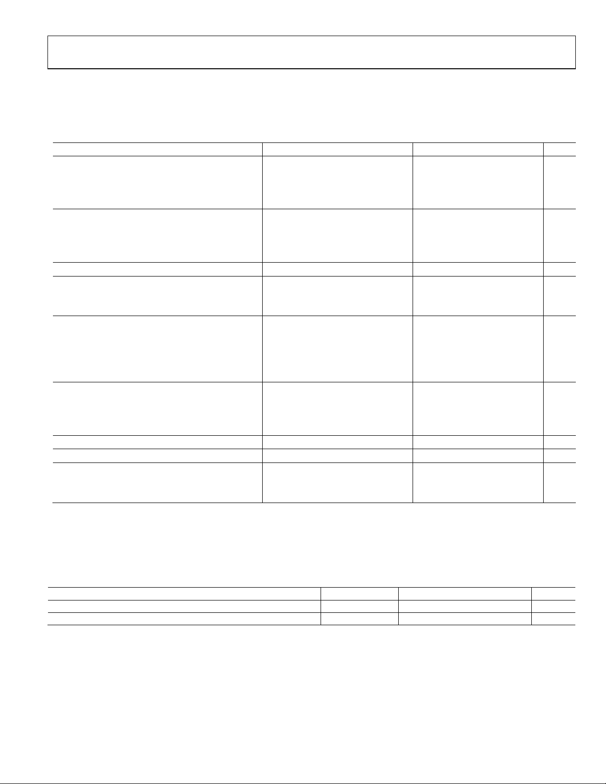
INPUT CHARACTERISTICS
VIN falling
2.00
2.15
2.25
V
Output Voltage Accuracy
PWM mode
−2 +2
%
SW On Resistance
PFET
155
240
mΩ
THERMAL CHARACTERISTICS
Parameter
Symbol
Min
Typ
Max
Unit
SPECIFICATIONS
VIN = 3.6 V, V
unless otherwise noted. All limits at temperature extremes are guaranteed via correlation using standard statistical quality control (SQC).
Table 1.
Parameter Test Conditions/Comments Min Typ Max Unit
Input Voltage Range 2.3 5.5 V
Undervoltage Lockout Threshold VIN rising 2.3 V
OUTPUT CHARACTERISTICS
Line Regulation VIN = 2.3 V to 5.5 V, PWM mode 0.25 %/V
Load Regulation I
PWM TO POWER SAVE MODE CURRENT THRESHOLD 100 mA
INPUT CURRENT CHARACTERISTICS
DC Operating Current I
Shutdown Current EN = 0 V, TA = TJ = −40°C to +85°C 0.2 1.0 μA
SW CHARACTERISTICS
= 0.8 V − 3.3 V, TJ = −40°C to +125°C for minimum/maximum specifications, and TA = 25°C for typical specifications,
OUT
= 0 mA − 800 mA −0.95 %/A
LOAD
= 0 mA, device not switching 23 30 μA
LOAD
NFET 115 200 mΩ
Current Limit PFET switch peak current limit 1100 1500 1650 mA
Discharge Switch (ADP2139) 100 Ω
ENABLE AND MODE CHARACTERISTICS
Input High Threshold 1.2 V
Input Low Threshold 0.4 V
Input Leakage Current EN/MODE = 0 V (min), 3.6 V (max ) −1 0 +1 μA
OSCILLATOR FREQUENCY 2.6 3.0 3.4 MHz
STAR T-UP TIME 250 μs
Thermal Shutdown Threshold 150 °C
Thermal Shutdown Hysteresis 20 °C
INPUT AND OUTPUT CAPACITOR, RECOMMENDED SPECIFICATIONS
TA = −40°C to +125°C, unless otherwise specified. All limits at temperature extremes are guaranteed via correlation using standard
statistical quality control (SQC).
Table 2.
MINIMUM INPUT AND OUTPUT CAPACITANCE C
CAPACITOR ESR R
4.7 µF
MIN
0.001 1 Ω
ESR
Rev. B | Page 3 of 20

ADP2138/ADP2139 Data Sheet
Machine
±100 V
ABSOLUTE MAXIMUM RATINGS
Table 3.
Parameter Rating
VIN, EN, MODE −0.4 V to +6.5 V
VOUT, SW to GND −1.0 V to (VIN + 0.2 V)
Temperature Range
Operating Ambient −40°C to +85°C
Operating Junction −40°C to +125°C
Storage Temperature −65°C to +150°C
Lead Temperature Range −65°C to +150°C
Soldering (10 sec) 300°C
Vapor Phase (60 sec) 215°C
Infrared (15 sec) 220°C
ESD Model
Human Body ±1500 V
Charged Device ±500 V
Stresses above those listed under Absolute Maximum Ratings
may cause permanent damage to the device. This is a stress
rating only; functional operation of the device at these or any
other conditions above those indicated in the operational
section of this specification is not implied. Exposure to absolute
maximum rating conditions for extended periods may affect
device reliability.
THERMAL DATA
Absolute maximum ratings apply individually only, not in
combination.
ADP2138/ADP2139 can be damaged when the junction temperature limits are exceeded. Monitoring ambient temperature does
not guarantee that the junction temperature (T
specified temperature limits. In applications with high power
dissipation and poor thermal resistance, the maximum ambient
temperature may need to be derated. In applications with moderate power dissipation and low printed circuit board (PCB)
thermal resistance, the maximum ambient temperature can
exceed the maximum limit for as long as the junction temperature
is within specification limits. The junction temperature (T
the device is dependent on the ambient temperature (T
power dissipation of the device (P
thermal resistance of the package (θ
temperature (T
(T
) and power dissipation (PD) using the formula
A
T
= TA + (PD × θJA)
J
) is calculated from the ambient temperature
J
), and the junction-to-ambient
D
). Maximum junction
JA
) is within the
J
) of
J
), the
A
Junction-to-ambient thermal resistance (θ
based on modeling and calculation using a 4-layer board. The
junction-to-ambient thermal resistance is highly dependent on
the application and board layout. In applications where high
maximum power dissipation exists, close attention to thermal
board design is required. The value of θ
PCB material, layout, and environmental conditions. The specified
values of θ
are based on a 4-layer, 4 in. × 3 in., circuit board. Refer
JA
to JEDEC JESD 51-9 for detailed information pertaining to board
construction. For additional information, see AN-617 Application Note, MicroCSP
Ψ
is the junction-to-board thermal characterization parameter
JB
measured in units of °C/ W. Ψ
TM
Wafer Level Chip Scale Package.
of the package is based on modeling
JB
and calculation using a 4-layer board. The JESD51-12, Guidelines
for Reporting and Using Package Thermal Information, states that
thermal characterization parameters are not the same as thermal
resistances. Ψ
measures the component power flowing through
JB
multiple thermal paths rather than through a single path, which
is the procedure for measuring thermal resistance, θ
fore, Ψ
thermal paths include convection from the top of the
JB
package as well as radiation from the package; factors that make
Ψ
more useful in real-world applications than θJB. Maximum
JB
junction temperature (T
(T
) and power dissipation (PD) using the formula
B
T
= TB + (PD × ΨJB)
J
) is calculated from the board temperature
J
Refer to JEDEC JESD51-8 and JESD51-12 for more detailed
information about Ψ
.
JB
THERMAL RESISTANCE
θJA and ΨJB are specified for the worst-case conditions, that is, a
device soldered in a circuit board for surface-mount packages.
Table 4. Thermal Resistance
Package Type θJA ΨJB Unit
6-Ball WLCSP 170 80 °C/W
ESD CAUTION
) of the package is
JA
may vary, depending on
JA
. There-
JB
Rev. B | Page 4 of 20

Data Sheet ADP2138/ADP2139
PIN CONFIGURATION AND FUNCTION DESCRIPTIONS
VIN EN
1
4
SW
MODE
2
5
GND VOUT
3
6
TOP VIEW
(BALL SI DE DOWN)
Not to Scale
Figure 2. Pin Configuration (Top View)
Table 5. Pin Function Descriptions
Pin No. Mnemonic Description
1 VIN
Power Source Input. VIN is the source of the PFET high-side switch. Bypass VIN to GND with a 4.7 μF or greater
capacitor as close to the ADP2138/ADP2139 as possible.
2 SW
Switch Node Output. SW is the drain of the P-channel MOSFET switch and N-channel synchronous rectifier.
Connect the output LC filter between SW and the output voltage.
3 GND Ground. Connect the input and output capacitors to GND.
4 EN Buck Activation. To turn on the buck, set EN to high. To turn off the buck, set EN to low.
5 MODE
Mode Input. Drive the MODE pin high for the operating mode to force continuous PWM switching. Drive the MODE
pin low to allow automatic PWM/PSM operating mode.
6 VOUT Output Voltage Sensing Input.
9496-002
Rev. B | Page 5 of 20

ADP2138/ADP2139 Data Sheet
100
90
80
70
60
50
40
30
20
10
0
0.001 0.01 0.1 1
I
OUT
(A)
EFFICIENCY (%)
09496-003
VIN = 2.3V
V
IN
= 3.6V
V
IN
= 4.2V
V
IN
= 5.5V
100
90
80
70
60
50
40
30
20
10
0
0.001 0.01 0.1 1
I
OUT
(A)
EFFICIENCY (%)
09496-004
VIN = 2.3V
V
IN
= 3.6V
V
IN
= 4.2V
VIN = 5.5V
100
90
80
70
60
50
40
30
20
10
0
0.001 0.01 0.1 1
I
OUT
(A)
EFFICIENCY (%)
09496-005
VIN = 2.3V
V
IN
= 3.6V
V
IN
= 4.2V
V
IN
= 5.5V
100
90
80
70
60
50
40
30
20
10
0
0.001 0.01 0.1 1
I
OUT
(A)
EFFICIENCY (%)
09496-006
V
IN
= 2.3V
V
IN
= 3.6V
V
IN
= 4.2V
V
IN
= 5.5V
100
90
80
70
60
50
40
30
20
10
0
0.001 0.01 0.1 1
I
OUT
(A)
EFFICIENCY (%)
09496-007
VIN = 3.9V
V
IN
= 4.2V
V
IN
= 5.5V
100
90
80
70
60
50
40
30
20
10
0
0.001 0.01 0.1 1
I
OUT
(A)
EFFICIENCY (%)
09496-008
VIN = 3.9V
V
IN
= 4.2V
V
IN
= 5.5V
TYPICAL PERFORMANCE CHARACTERISTICS
VIN = 3.6 V, TA = 25°C, VEN = VIN, unless otherwise noted.
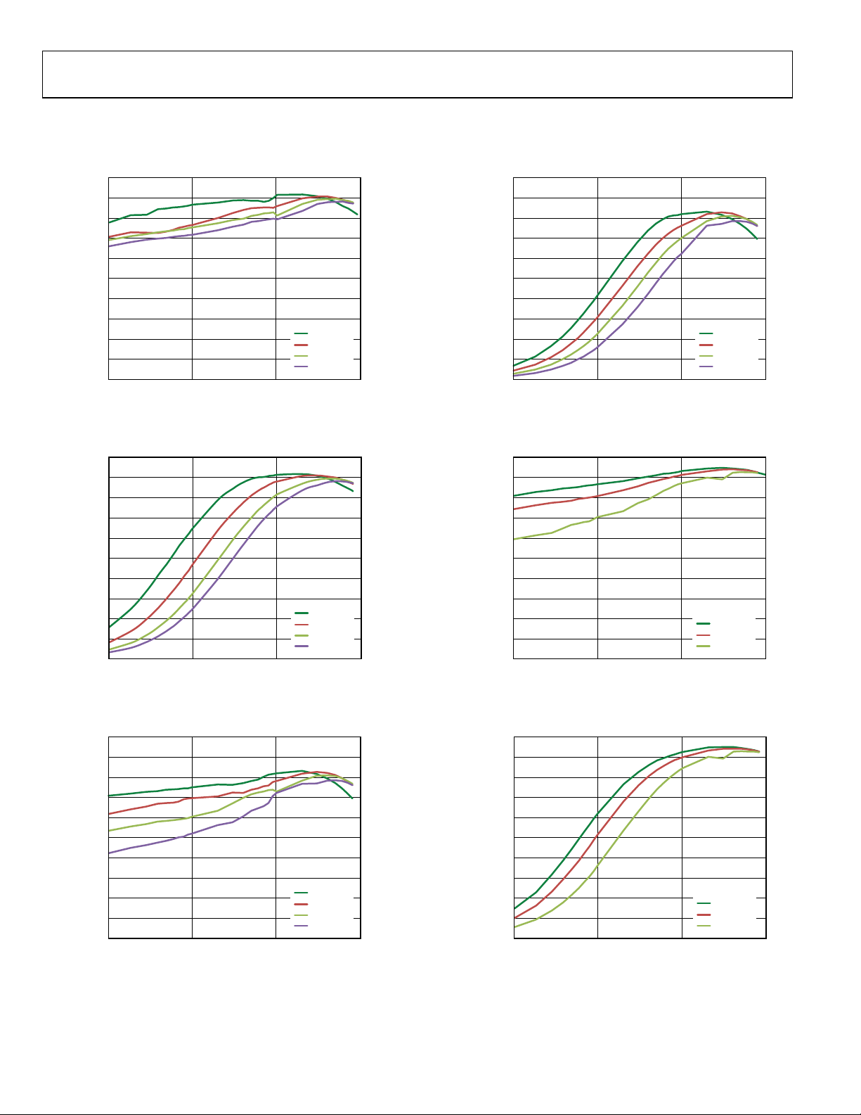
Figure 3. Efficiency vs. Load Current, Across Input Voltage,
V
= 1.8 V, PSM Mode
OUT
Figure 4. Efficiency vs. Load Current, Across Input Voltage,
V
= 1.8 V, PWM Mode
OUT
Figure 6. Efficiency vs. Load Current, Across Input Voltage,
V
= 0.8 V, PWM Mode
OUT
Figure 7. Efficiency vs. Load Current, Across Input Voltage,
V
= 3.3 V, PSM Mode
OUT
Figure 5. Efficiency vs. Load Current, Across Input Voltage,
V
= 0.8 V, PSM Mode
OUT
Figure 8. Efficiency vs. Load Current, Across Input Voltage,
V
= 3.3 V, PWM Mode
OUT
Rev. B | Page 6 of 20
 Loading...