

500 mA, 6 MHz, Synchronous
www.BDTIC.com/ADI
Preliminary Technical Data
FEATURES
92 % peak efficiency
6 MHz operating frequency
38 µA (typical) no load quiescent current in PFM mode
1.80 V, 1.82 V, 1.85V, 1.875V fixed output voltage
500 mA continuous output current
Input voltage :2.3 V to 5.5 V
0.28 µA (typical) shutdown supply current
Automatic power-saving mode
Compatible with tiny multilayer inductors
Internal synchronous rectifier
Internal compensation
Internal soft start
Output to ground short circuit protection
Current-limit protection
Enable/shutdown logic input
Undervoltage lockout
Thermal shutdown
Ultra small 6-ball 1.17 mm
APPLICATIONS
Mobile phones
Digital cameras
Digital audio
Portable equipment
1-cell Li+/Li-polymer and 3-cell alkaline/nickel
2
WLCSP
Step-Down, DC-to-DC Converter
ADP2121
GENERAL DESCRIPTION
The ADP2121 is a high frequency, low quiescent current, stepdown, dc-to-dc converter optimized for portable applications in
which board area and battery life are critical constraints. Fixed
frequency operation at 6 MHz enables the use of tiny ceramic
inductors and capacitors. Additionally the synchronous rectification
improves efficiency and results in fewer external components. At
high load currents, the device uses a voltage regulating pulse-width
modulation (PWM) mode that maintains a constant frequency
with excellent stability and transient response. At light load
conditions, the ADP2121 can automatically enter a power saving
mode that utilizes pulse-frequency modulation (PFM) to reduce
the effective switching frequency and ensure the longest battery
life in portable applications. During logic controlled shutdown
(EN = 0), the input is disconnected from the output and draws less
than 0.28 A (typical) from the source.
The ADP2121 has an input voltage range of 2.3 V to 5.5 V allowing the
use of a single Li+/Li-polymer cell, multiple alkaline/Ni-MH cell,
PCMCIA, and other standard power sources. The converter is
internally compensated to minimize external components, and its 1.80
V, 1.82 V, 1.85 V, or 1.875 V fixed output can source up to 500 mA.
Other key features include undervoltage lockout (UVLO) to prevent
deep-battery discharge and soft start to prevent input current
overshoot at startup.
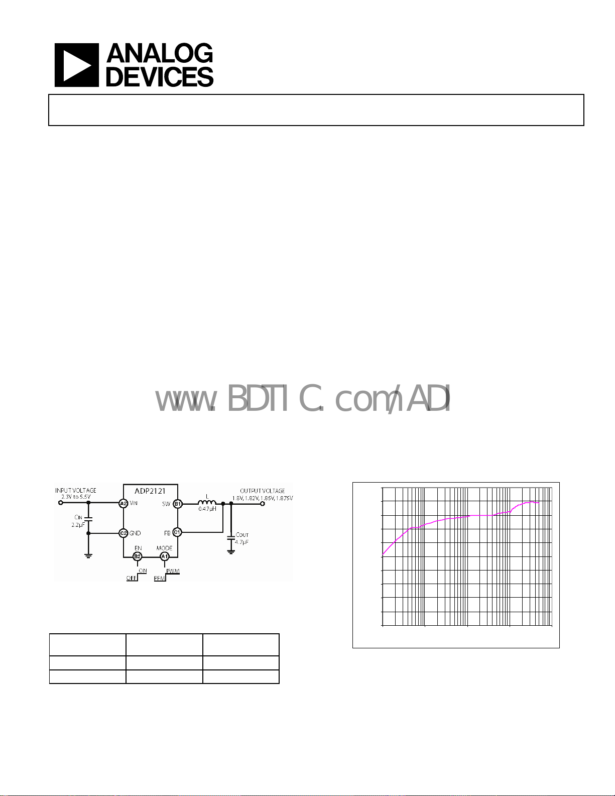
TYPICAL APPLICATION CIRCUIT
Figure 1. Circuit Configuration of ADP2121
OUTPUT VOLTAGE OPTIONS
Table 1.
Input Voltage
Range (V)
2.3 - 5.5 100 1.800, 1.850, 1.875
2.3 - 5.5 300 1.820
Rev. PrA
Information furnished by Analog Devices is believed to be accurate and reliable. However, no
responsibility is assumed by Analog Devices for its use, nor for any infringements of patents or other
rights of third parties that may result from its use. Specifications subject to change without notice. No
license is granted by implication or otherwise under any patent or patent rights of Analog Devices.
Trademarks and registered trademarks are the property of their respective owners.
Maximum Start-
up Time (s)
Fixed Output
Voltage (V)
TYPICAL PERFORMANCE
10 0 %
90%
80%
70%
60%
50%
40%
Efficiency
30%
20%
10 %
0%
0 .1 1 10 10 0 10 0 0
Figure 2. Efficiency vs. Load Current (V
One Technology Way, P.O. Box 9106, Norwood, MA 02062-9106, U.S.A.
Tel: 781.329.4700 www.analog.com
Fax: 781.461.3113 ©2008 Analog Devices, Inc. All rights reserved.
Load C urre nt ( mA )
= 3.6 V, V
IN
= 1.82 V, Auto Mode)
OUT

ADP2121 Preliminary Technical Data
www.BDTIC.com/ADI
TABLE OF CONTENTS
Features.............................................................................................. 1
Applications....................................................................................... 1
General Description ......................................................................... 1
Typical Application Circuit ............................................................. 1
Typical Performance......................................................................... 1
Revision History ............................................................................... 2
Specifications..................................................................................... 3
Absolute Maximum Ratings............................................................ 4
Thermal Resistance ...................................................................... 4
ESD Caution.................................................................................. 4
Pin Configuration and Function Descriptions............................. 5
Typical Performance Characteristics ............................................. 6
REVISION HISTORY
11/08—Revision PrA: Preliminary Version
Theory of Operation .........................................................................8
Overview ........................................................................................8
Mode Selection ..............................................................................8
Enable/Shutdown..........................................................................9
Internal Control Features.............................................................9
Applications Information.............................................................. 11
Inductor Selection...................................................................... 11
Input Capacitor Selection.......................................................... 11
Output Capacitor Selection ...................................................... 11
PCB Layout Guide.......................................................................... 13
Outline Dimensions....................................................................... 14
Ordering Guide .......................................................................... 14
Rev. PrA | Page 2 of 14

Preliminary Technical Data ADP2121
www.BDTIC.com/ADI
SPECIFICATIONS1
VIN = EN = 3.6 V, all values are at TA = 25°C.
Table 2.
Parameters Conditions Min Typ Max Unit
SUPPLY
Input Voltage Range I
I
Quiescent Current VIN = 3.6 V (PFM mode), no load, TA = 85°C 38 55 µA
V
Shutdown Current VEN = 0 V 0.28 0.5 µA
UNDERVOLTAGE LOCKOUT
Undervoltage Lockout Threshold VIN rising 2.2 V
V
OUTPUT
Continuous Output Current VIN = 2.3 V 400 mA
V
2
Feedback Bias Current VFB = 1.8 V 3.8 µA
SWITCHING CHARACTERISTICS
)
DSon
SW Leakage Current VIN = 5.5 V, V
SW Current Limit P-channel switch 850 1000 1150 mA
Oscillator Frequency 5.4 6 6.6 MHz
EFFICIENCY (VIN = 3.6 V, V
= 1.82 V) L = 0.47 H, C
OUT
I
I
I
I
I
EN/MODE INPUT LOGIC
High Threshold Voltage 1.2 V
Low Threshold Voltage 0.4 V
Leakage Current VEN = V
SOFT START
3
C
Soft Start Period V
THERMAL SHUTDOWN
Thermal Shutdown Threshold 150 °C
Thermal Shutdown Hysteresis 30 °C
= 0 mA to 400 mA 2.3 5.5 V
LOAD
= 0 mA to 500 mA 2.5 5.5
LOAD
= 3.6 V (PWM mode), no load 10 mA
IN
falling 1.8 V
IN
= 2.5 V to 5.5V 500 mA
IN
Auto mode - 2% V
PWM mode - 2% V
+ 3% V Output Accuracy (1.82 V, VIN = 3.6)
NOM
+ 3% V
NOM
P-channel switch 225 440 m SW On Resistance (R
N-channel synchronous rectifier 290 810 m
= 0 V, 5.5 V 1 µA
SW
= 4.7 F
OUT
= 10 mA (PFM mode) 79 %
LOAD
= 50 mA (PFM mode) 81 %
LOAD
= 150 mA (PWM mode) 87 %
LOAD
= 250 mA (PWM mode) 89 %
LOAD
= 500 mA (PWM mode) 89 %
LOAD
= 0.5 V, 5.5 V 0.01 1 µA
MODE
= 4.7 F, VIN = 3.6 V (time from EN = 0 to stable
OUT
V
)
OUT
= 1.82 V
OUT
V
= 1.8 V, 1.85 V, 1.875 V
OUT
270
80
300
100
µs
µs
1
All limits are subject to change upon final temperature characterization and release.
2
Transients not included in voltage accuracy specifications. For PFM mode, the V
3
Guaranteed by design.
accuracy specification is for the lower point of the ripple.
OUT
Rev. PrA | Page 3 of 14
ADP2121 Preliminary Technical Data
www.BDTIC.com/ADI
ABSOLUTE MAXIMUM RATINGS
Table 3.
Parameter Rating
VIN −0.3 V to +6 V
VEN/V
VFB/VSW −0.3 V to VIN + 0.2 V
Operating Ambient Temperature –40°C to +85°C
Operating Junction Temperature –40°C to + 125°C @ 500 mA
Storage Temperature –45°C to +150°C
Soldering (10 sec) 300°C
Vapor Phase (60 sec) 215°C
Infrared (15 sec) 220°C
ESD (electrostatic discharge)
Stresses above those listed under Absolute Maximum Ratings
may cause permanent damage to the device. This is a stress
rating only; functional operation of the device at these or any
other conditions above those indicated in the operational
section of this specification is not implied. Exposure to absolute
maximum rating conditions for extended periods may affect
device reliability.
−0.3 V to +6 V
MODE
Machine Model −100 V to +100 V
Human Body Model −2000 V to +2000 V
Charged Device Model −500 V to +500 V
THERMAL RESISTANCE
The thermal resistance of the system, θJA, is specified for the
worst-case conditions, that is, a device soldered in a circuit
board for surface-mount packages. The junction-to-ambient
thermal resistance is highly dependent on the application and
board layout. In applications where high maximum power
dissipation exists, attention to thermal board design is required.
The value of θ
and environmental conditions.
Table 4.
Package Type θ
6-Ball WLCSP
2-Layer Board 105 °C/W
4-Layer Board 198 °C/W
Maximum Power Dissipation
2-Layer Board 380 mW
4-Layer Board 202 mW
may vary, depending on PCB material, layout,
JA
Unit
JA
ESD CAUTION
Rev. PrA | Page 4 of 14
Preliminary Technical Data ADP2121
www.BDTIC.com/ADI
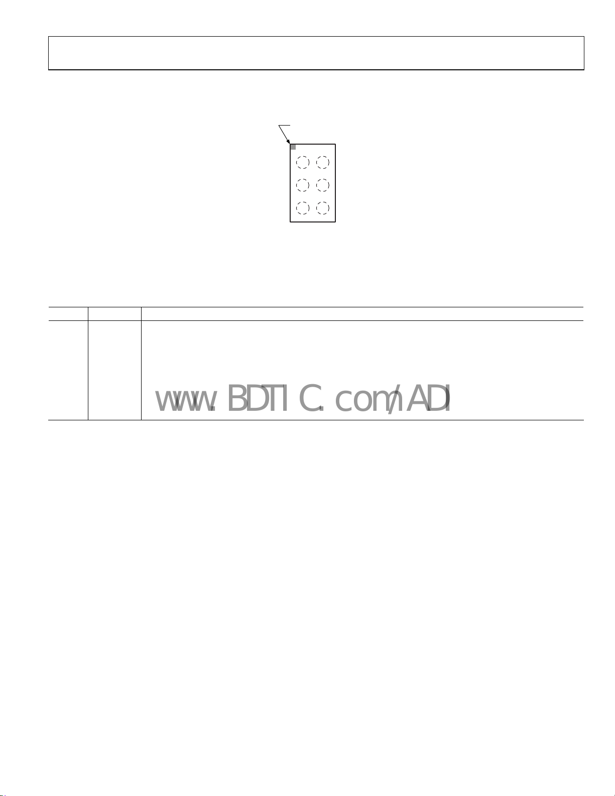
PIN CONFIGURATION AND FUNCTION DESCRIPTIONS
BALLA1
INDICATOR
1
2
MODE VIN
A
SW
B
C
(BALL SIDE DOW N)
(BUMPS ON OPPOSITE SIDE)
Figure 3. Pin Configuration
Table 5. Pin Function Descriptions
Pin No. Mnemonic Description
A1 MODE Mode Select. This pin toggles between auto (PFM and PWM switching) and PWM modes. Set MODE low to allow
the part to operate in auto mode. Pull MODE high to force the part to operate in PWM mode.
B1 SW Switch Node.
C1 FB Feedback Divider Input. Connect the output capacitor from FB to GND to set the output voltage ripple and to
complete the control loop.
A2 VIN Power Supply Input.
B2 EN Enable. Pull this pin high to enable the part. Set this pin low to disable the part. Do not leave this pin floating.
C2 GND Ground Pin.
EN
FB GND
TOP VIEW
Not to Scale
07407-003
Rev. PrA | Page 5 of 14

ADP2121 Preliminary Technical Data
(
)
www.BDTIC.com/ADI
TYPICAL PERFORMANCE CHARACTERISTICS
10 0 %
90%
80%
70%
60%
50%
40%
Efficiency
30%
20%
10 %
0%
0 .1 1 10 10 0 10 0 0
VIN = 3.6 V
VIN = 2.3 V
Load C urre nt ( mA )
VIN = 4.2 V
Figure 4. Efficiency vs. Load Current (Auto Mode, V
1.9 0 0
1.8 9 0
1.8 8 0
1.8 70
1.8 6 0
1.8 50
1.8 4 0
VIN = 2.3 V
1.8 3 0
Output Voltage (V)
1.8 2 0
1.8 10
1.8 0 0
0.1 1 10 100 1000
VIN = 3.6 V
Load C urre nt ( mA)
VIN = 5.5 V
Figure 5. Output Voltage Accuracy (Auto Mode, V
VIN = 5.5 V
= 1.82 V)
OUT
VIN = 4.2 V
= 1.82 V)
OUT
10 0 %
90%
VIN = 2.3 V
80%
70%
60%
50%
40%
Efficiency
30%
20%
10 %
0%
1 10 100 1000
Load C urre nt ( mA)
VIN = 5.5 V
VIN = 3.6 V
VIN = 4.2 V
Figure 7. Efficiency vs. Load Current (PWM Mode, V
1.9 0 0
1.8 9 0
1.8 8 0
1.8 70
1.8 6 0
1.8 50
1.8 4 0
1.8 3 0
VIN = 4.2 V
1.8 2 0
Output Voltage (V)
1.8 10
VIN = 2.3 V
1.8 0 0
1 10 100 1000
VIN = 5.5 V
= 1.82 V)
OUT
VIN = 3.6 V
Load C urrent ( mA )
Figure 8. Output Voltage Accuracy (PWM Mode, V
= 1.82 V)
OUT
V
(20m V/DIV, 1.82 V Offs et)
OUT
SW
(2V/DIV)
= 3.6 V
V
IN
= 1.82 V
V
OUT
I
= 25 mA
OUT
I
L
(200m A/DIV)
t (1.0µs/DIV)
Figure 6. PFM Mode Operation
Rev. PrA | Page 6 of 14
VIN = 3.6 V, V
V
(20m V /DIV, 1.82 V DC Offs e t)
OUT
SW (5V/DIV)
I
(200m A/DIV)
L
t
100ns /DIV
Figure 9. PWM Mode Operation
= 1.82 V, I
OUT
= 200 mA
OUT
Preliminary Technical Data ADP2121
www.BDTIC.com/ADI
= 1.82 V
V
OUT
V
OUT
(1V/DIV)
EN
(2V/DIV)
I
L
(200m A/DIV)
= 3.6 V
V
IN
= 1.82 V
V
OUT
No L o ad
V
(100m V/DIV)
OUT
(1A/DIV)
I
L
t (40µs/DIV)
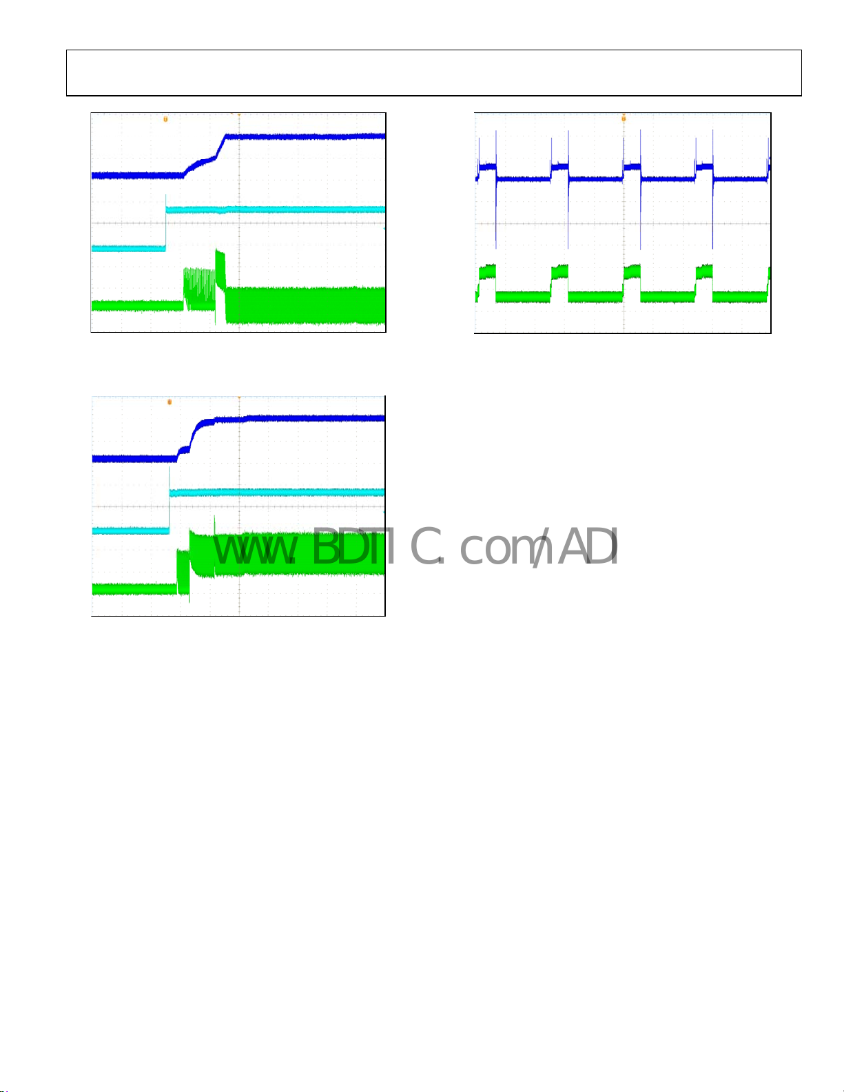
Figure 10. Start-Up Waveform (No Load, VIN = 3.6 V, V
V
OUT
(1V/DIV)
EN
(2V/DIV)
I
L
(200m A/DIV)
t (100µs/DIV)
Figure 11. Start-Up Waveform (R
= 5.1 Ω, VIN = 3.6 V, V
LOAD
V
V
R
IN
OUT
LOAD
= 1.82 V)
OUT
= 3.6 V
= 1.82 V
= 5.1 Ω
= 1.82 V)
OUT
t (1.0ms/DIV)
Figure 12. Output Short Circuit Response
Rev. PrA | Page 7 of 14

ADP2121 Preliminary Technical Data
V
V
www.BDTIC.com/ADI
THEORY OF OPERATION
BAT
OUT
FB
C1
R1
R2
AGND
REF
BANDGAP
EAMP
BG
COMPENSATION
PFM
COMPARATOR
BG
B2
PFM
EN
ANGD
6MHz
OSCILLATOR
THRESHOLD
DETECT
RAMP
V(V
SHUTDOWN
SOFT ST ART
A1
MODE
PWM
COMP
EAMP
IN)
THERMAL
THRESHOLD
DETECT
2.3 TO 5. 5V
SHOOTTHROUG H
CONTROL
LOGIC
AND
PWM/PFM
CONTROL
PLLIM
ZXCOMP
DETECT
2.2µF
X5R
6V3
PDRIVE
NDRIVE
PFM
AV
PV
IN
IN
PREF
NREF
VIN
V
FB
A2
SW
470nH
B1
PGND
GND
C2
AGND
IN
4.7µF
X5R
6V3
V
OUT
Figure 13. Internal Block Diagram
OVERVIEW
The ADP2121 is a high efficiency, synchronous, step-down, dcto-dc converter that operates from a 2.3 V to 5.5 V input voltage.
It provides up to 500 mA of continuous output current at a fixed
1.80 V, 1.82 V, 1.85 V, or 1.875 V (typical) output voltage. The 6
MHz operating frequency enables the use of tiny external
components. The internal control schemes of the ADP2121 give
excellent stability and transient response. External control for
mode selection and part enabling provides power-saving options
that are aided by internal features such as synchronous
rectification and compensation. Other internal features such as
current limit, soft start, undervoltage lockout, output-to-ground
short circuit protection, and thermal shutdown provide
protection for internal and external circuit components.
MODE SELECTION
The ADP2121 has two modes of operation, determined by the
state of the MODE pin: auto and PWM.
Pull the MODE pin high to force the converter to operate in
PWM mode, regardless of the output current. Otherwise, set
MODE low to allow the converter to automatically enter the
power saving PFM mode at light load currents. Do not leave this
pin floating.
07407-034
Pulse-Width Modulation (PWM) Mode
The PWM mode forces the part to maintain a fixed frequency
of 6 MHz (typical) over all load conditions. The converter
controls the amount of power delivered to the load by varying
the duty cycle of the internal oscillator. This control provides
excellent stability, transient response, and output regulation,
but results in lower efficiencies at light load currents.
= 3.6 V, V
V
IN
V
(20m V /DIV, 1.82 V DC Offs e t)
OUT
SW (5V/DIV)
I
(200m A/DIV)
L
t (100ns /DIV)
Figure 14. Typical PWM Operation (V
= 1.82 V, I
OUT
= 3.6 V, V
IN
= 1.82V, I
OUT
= 200 mA
OUT
LOAD
= 150 mA)
Rev. PrA | Page 8 of 14

Preliminary Technical Data ADP2121
www.BDTIC.com/ADI
Auto Mode (PFM-PWM Switching)
Auto mode is a power saving feature that enables the converter to
switch between PWM and PFM in response to the output load.
The ADP2121 operates in PFM mode for light load currents and
switches to PWM mode for medium and heavy load currents
(Figure 15).
V
(20m V/DIV, 1.82 V Offs et)
OUT
SW
(2V/DIV)
I
L
(200m A/DIV)
= 3.6 V
V
IN
V
OUT
I
= 25 mA
OUT
= 1.82 V
Figure 15. PFM-to-PWM Transition Point
Pulse-Frequency Modulation
When the converter is operating under light load conditions, the
effective switching frequency and supply current are decreased
and varied using PFM to regulate the output voltage. This results
in improved efficiencies and lower quiescent currents. In PFM
mode, as shown in Figure 16, the converter only switches when
necessary to keep the output voltage within the PFM limits set by
an internal comparator. Switching stops when the upper limit is
reached and resumes when the lower limit is reached.
Once the upper level is reached, the output stage and oscillator
turn off to reduce the quiescent current. During this stage, the
output capacitor supplies the current to the load. As the output
capacitor discharges and the output voltage reaches the lower
PFM comparator threshold, switching resumes and the process
repeats. The output voltage, switching node voltage, and inductor
current during this process are shown in Figure 16.
t (1.0µs/DIV)
Figure 16. Typical PFM Operation (V
= 3.6 V, V
IN
= 1.82V, I
OUT
LOAD
= 25 mA)
Mode Transition
The converter switches between PFM and PWM automatically
to maintain optimal transient response and efficiency. The
mode transition point depends on input voltage. Hysteresis
exists in the transition point to prevent instability and
decreased efficiencies that could result if the converter were
able to oscillate between PFM and PWM for a fixed input
voltage and load current.
A switch from PFM to PWM occurs when the output voltage
dips below the lower PFM comparator threshold. Switching to
PWM allows the converter to maintain efficiency and supply a
heavier current to the load.
A switch from PWM to PFM occurs when the converter
outputs a decreased peak current for multiple consecutive
switching cycles. Switching to PFM allows the converter to
save power and supply a lighter load current with fewer
switching cycles.
Figure 16 shows the threshold voltage in PFM mode is slightly
higher to ensure that the converter is able to supply enough
current when transitioning into PWM mode.
ENABLE/SHUTDOWN
The EN input turns the ADP2121 on or off. Connect EN to
PGND or logic low to shut down the part and reduce the
current consumption to 0.1 µA (typical). Connect EN to VIN
or logic high to enable the part. Do not leave this pin floating.
INTERNAL CONTROL FEATURES
Overcurrent Protection
To ensure that excessively high currents do not damage the
inductor, the ADP2121 incorporates cycle-by-cycle overcurrent
protection. This function is accomplished by monitoring the
instantaneous peak current on the power PMOS switch. If this
current exceeds the maximum level (1 A typical), then the
PMOS is immediately turned off. This minimizes the potential
Rev. PrA | Page 9 of 14

ADP2121 Preliminary Technical Data
www.BDTIC.com/ADI
for damage to power components during certain faults and
transient events.
Soft Start
To prevent excessive input inrush current at startup, the
ADP2121 operates with an internal soft start. When EN goes
high, or when the part recovers from a fault (UVLO, TSD, or
short-circuit protection), a soft start timer begins. The soft start
timer corresponds to the maximum soft start period for the given
fixed output voltage. During this time, the peak current limit is
gradually increased to its maximum. As seen in the start-up
waveforms in the Typical Performance Characteristics, the output
voltage passes through several stages to ensure that each stages of
the converter is able to startup effectively and in proper sequence.
After the soft start period has expired, the peak current limit
remains at 1 A (typical) and the part enters the operating mode
determined by the MODE pin.
Synchronous Rectification
In addition to the P-channel MOSFET switch, the ADP2121
includes an N-channel MOSFET synchronous rectifier. The
synchronous rectifier improves efficiency, especially for small
load currents, and reduces cost and board space by eliminating
the need for an external rectifier.
erratic operation at low input voltages. The UVLO levels have
approximately 100 mV of hysteresis to ensure glitch-free
startup.
Output Short Circuit Protection
If the output voltage is inadvertently shorted to GND, a
standard dc-to-dc controller would deliver maximum power
into that short. This could result in a potentially catastrophic
failure. To prevent this, the ADP2121 senses when the output
voltage is below the SCP threshold (typically 1.2 V). At this
point, the controller turns off for approximately 1.8 ms and
then automatically initiates a soft start sequence. This cycle
repeats until the short is removed or the part is disabled. This
dramatically reduces the power delivered into the short circuit,
yet still allows the converter to recover if the fault is removed.
= 1.82 V
V
(100m V/DIV)
OUT
V
OUT
Compensation
The control loop is internally compensated to deliver maximum
performance with no additional external components. The error
amplifier compares the regulated output voltage on the feedback
pin (FB) to an internal reference voltage. The ADP2121 has been
designed to work with 0.47 H chip inductors and 4.7 F
capacitors (see
performance and/or stability.
Table 6 and Ta b le 7.) Other values may reduce
Undervoltage Lockout (UVLO)
If the input voltage is below the UVLO threshold, the ADP2121
automatically turns off the power switches and places the part
into a low power consumption mode. This prevents potentially
(1A/DIV)
I
L
t (1.0ms/DIV)
Figure 17. Output Short Circuit Protection
Thermal Shutdown (TSD) Protection
The ADP2121 also includes TSD protection. If the die
temperature exceeds 150°C (typical), the TSD protection
activates and turn off the power devices. They remain off until
the die temperature falls below 120°C (typical), at which point
Rev. PrA | Page 10 of 14

Preliminary Technical Data ADP2121
(
)
−
www.BDTIC.com/ADI
APPLICATIONS INFORMATION
The external component selection for the ADP2121
applications circuit is driven by the load requirement and
begins with the selection of Inductor L (see ). Once
the inductor is chosen, C
and C
IN
can be selected.
OUT
INDUCTOR SELECTION
The high switching frequency of the ADP2121 allows for minimal
output voltage ripple, even with small inductors. Inductor sizing
is a trade-off between efficiency and transient response. A small
inductor leads to a larger inductor current ripple that provides
excellent transient response, but degrades efficiency. Due to the
high switching frequency of the ADP2121, multilayer ceramic
inductors can be used for an overall smaller solution size. Shielded
ferrite core inductors are recommended for their low core losses
and low electromagnetic interference (EMI).
As a guideline, the inductor peak-to-peak current ripple is
typically set to
I
= 0.45 × I
L
where I
LOAD
current, I
L
IDEAL
where f
SW
is the maximum output current. The largest ripple
, occurs at the maximum input voltage.
L
=
is the switching frequency.
(1)
LOAD
()
VVV
−×
IN
OUT
() ()
SW
MAXIN
OUT
IfV
×××
45.0
(2)
MAXLOAD
It is important that the inductor be capable of handling the
maximum peak inductor current, I
, determined by the
PK
following equation:
I
PK
= I
LOAD(MAX)
+ IL/2 (3)
The dc current rating of the inductor should be at least equal
to the maximum load current plus half the ripple current to
prevent core saturation.
Table 6 shows some typical surface
mount inductors that work well in ADP2121 applications.
INPUT CAPACITOR SELECTION
The input capacitor must be able to support the maximum
input operating voltage and the maximum rms input current.
The maximum rms input current flowing through the input
capacitor is at maximum I
capable of withstanding the rms input current for the maximum
load current in the application using the following equation:
IrmsI
OUTMAX
The input capacitor reduces the input voltage ripple caused by
the switch currents on the VIN pin. Place the input capacitor as
close as possible to the VIN pin.
/2. Select an input capacitor
OUT
()
VVV
−×
OUT
×=
IN
V
IN
OUT
(4)
In principle, different types of capacitors can be considered,
but for battery-powered applications, the best choice is the
multilayer ceramic capacitor, due to its small size and
equivalent series resistance (ESR).
Table 7 offers input capacitor
suggestions.
It is recommended that the VIN pin be bypassed with a 2.2 µF
or larger ceramic input capacitor if the supply line has a
distributed capacitance of at least 10 F. If not, at least a 10 F
capacitor is recommended on the input supply pin. The input
capacitor can be increased without any limit for better input
voltage filtering. X5R or X7R dielectrics are recommended, with a
voltage rating of 6.3 V or 10 V. Y5U and Z5U dielectrics are not
recommended, due to their poor temperature and dc bias
characteristics.
OUTPUT CAPACITOR SELECTION
The output capacitor selection affects both the output voltage
ripple and the loop dynamics of the converter. For a given loop
crossover frequency (the frequency at which the loop gain
drops to 0 dB), the maximum voltage transient excursion
(overshoot) is inversely proportional to the value of the output
capacitor. The ADP2121 has been designed to operate with
small ceramic capacitors in the 4.7 µF to 10 µF range that have
low ESR and equivalent series inductance (ESL) and are able,
therefore, to meet tight output voltage ripple specifications. X5R
or X7R dielectrics are recommended with a voltage rating of 6.3
Table 7 shows a list of input and output MLCC capacitors
V.
recommended for ADP2121 applications.
When choosing output capacitors, it is also important to
account for the loss of capacitance due to output voltage dc bias.
This may result in using a capacitor with a higher rated voltage
to achieve the desired capacitance value. Additionally, if
ceramic output capacitors are used, the capacitor rms ripple
current rating should always meet the application requirements.
The rms ripple current is calculated as:
rmsI
()
COUT
1
32
×
OUT
×= (5)
SW
At nominal load currents, the converter operates in forced
frequency (PWM) mode, and the overall output voltage ripple is
the sum of the voltage spike caused by the output capacitor ESR
plus the voltage ripple caused by charging and discharging the
output capacitor.
= IL × (ESR + 1/(8 × C
V
OUT
OUT
The largest voltage ripple occurs at the highest input voltage,
V
. At light load currents, if MODE is set low, then the
IN
converter operates in power save (PFM) mode and the output
voltage ripple increases.
VVV
OUT
)(
MAXIN
××
VfL
)(
MAXIN
× fSW)) (6)
Rev. PrA | Page 11 of 14

ADP2121 Preliminary Technical Data
www.BDTIC.com/ADI
Table 6. Recommended Inductor Selection
Manufacturer Series Inductance (µH) DCR (Ω) Current Rating (mA) Size (L × W × H) (mm) Package
Murata LQM2HP_G0 0.47 ± 20% 0.040 ± 25% 1800 2.5 × 2.0 × 0.90 1008
LQM21PNR47MC0D 0.47 ± 20% 0.120 ± 25% 1100 2.0 × 1.25 × 0.50 0805
Taiyo Yuden
Table 7. Recommended Input and Output Capacitor Selection
Manufacturer Capacitance (F) Voltage Rating (V)
Input
Murata 2.2 6.3 X5R GRM155R60J225M 1.0 × 0.5 × 0.5 0402
Taiyo Yuden 2.2 6.3 X5R JMK105BJ225MV-F 1.0 × 0.5 × 0.5 0402
Panasonic 2.2 6.3 X5R ECJ-0EB0J225M 1.0 × 0.5 × 0.5 0402
Output
Murata 4.7 6.3 X5R GRM188R60J475K 1.6 × 0.8 × 0.8 0603
Taiyo Yuden 4.7 4 X5R AMK105BJ475MV-F 1.0 × 0.5 × 0.5 0402
Panasonic 4.7 6.3 5R
BRC1608TR45M
0.45 ± 20% 0.117 ± 30% 800 1.6 × 0.8 × 0.8 0603
Temperature
Coefficient Part Number Size (L × W × H) (mm) Package
ECJ-0EB0J475M
1.0 × 0.5 × 0.5 0402
Rev. PrA | Page 12 of 14

Preliminary Technical Data ADP2121
www.BDTIC.com/ADI
PCB LAYOUT GUIDE
MODE
ADP2121
2.0mm
Figure 18. Example Layout for an ADP2121 Application
SW
L1
VOUT
C2
2.65mm
VIN
GND
C1EN
07407-039
For high efficiency, good regulation, and stability with the
ADP2121, a well-designed printed circuit board layout is
required.
Use the following guidelines when designing printed
circuit boards:
• Keep the low ESR input capacitor, C
, close to VIN and GND.
IN
• Keep high current traces as short and as wide as possible.
• Avoid routing high impedance traces near any node
connected to SW or near the inductor to prevent radiated
noise injection.
Rev. 0 | Page 13 of 14
www.BDTIC.com/ADI
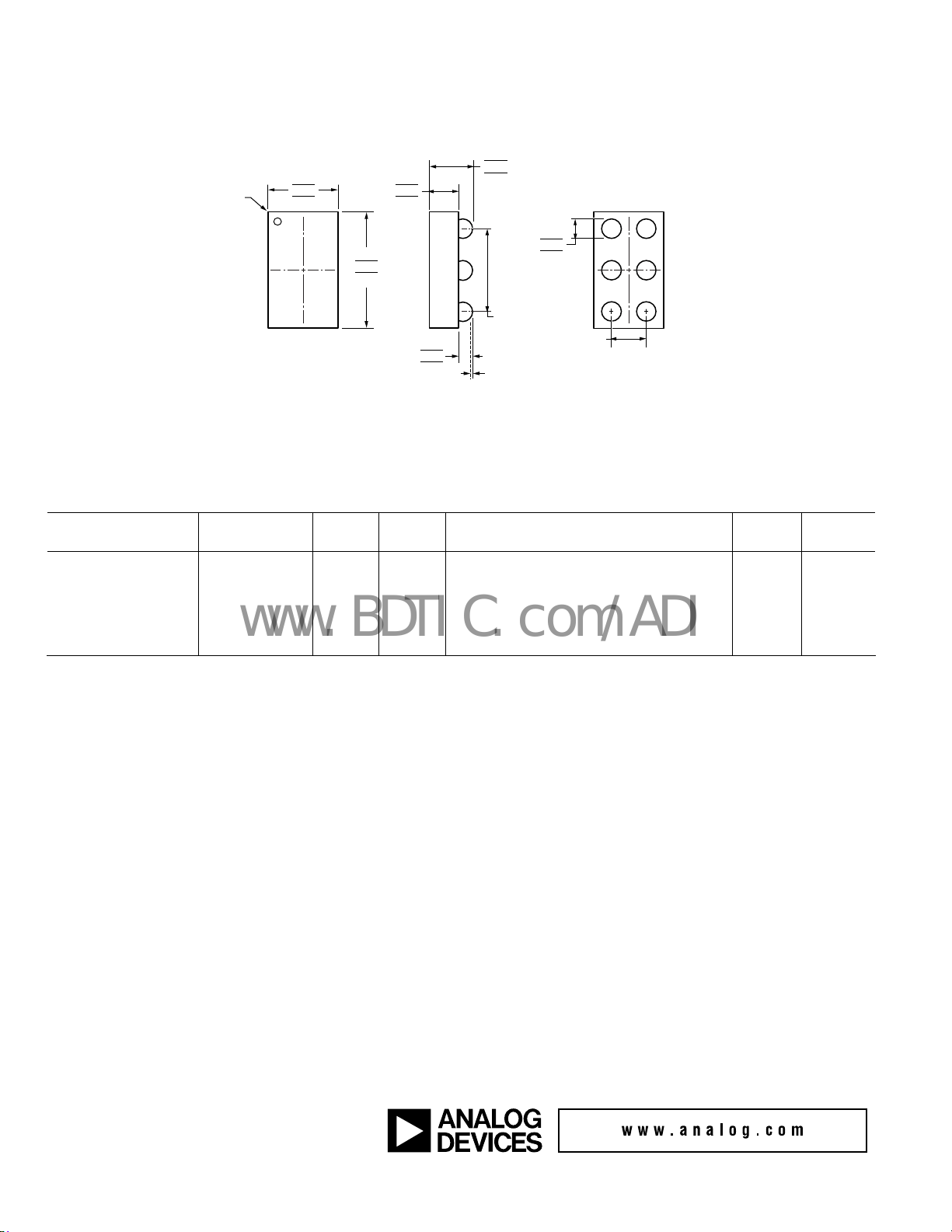
OUTLINE DIMENSIONS
A1 BALL
CORNER
0.940
0.900
0.860
1.340
1.300
1.260
0.430
0.400
0.370
0.660
0.600
0.540
0.280
0.260
0.240
12
A
B
C
021908-A
TOP VIEW
(BALL SI DE DOWN)
0.230
0.200
0.170
0.800
BSC
0.075 NOM
COPLANARITY
0.400 BSC
BALL PITCH
BOTTOM VIEW
(BALL SIDE UP)
Figure 19. 6-Ball Wafer Level Chip Scale Package (WLCSP)
(CB-6-4)
Dimensions shown in millimeters
ORDERING GUIDE
Te mp e ra tu r e
Model
ADP2121YCBZ-1.80R7
ADP2121YCBZ-1.82R7
ADP2121YCBZ-1.85R7
ADP2121YCBZ- −40 °C to +85 °C 1.875 V 80 s 6-Ball Wafer Level Chip Scale Package [WLCSP] CB-6-4 L95
4
1.875R7
Range
1
−40 °C to +85 °C 1.800 V 80 s 6-Ball Wafer Level Chip Scale Package [WLCSP] CB-6-4 L92
2
−40 °C to +85 °C 1.820 V 270 s 6-Ball Wafer Level Chip Scale Package [WLCSP] CB-6-4 L93
3
−40 °C to +85 °C 1.850 V 80 s 6-Ball Wafer Level Chip Scale Package [WLCSP] CB-6-4 L94
1
Z = RoHS Compliant Part.
2
Z = RoHS Compliant Part.
3
Z = RoHS Compliant Part.
4
Z = RoHS Compliant Part.
Output
Voltage
Startup
Time Package Description
Package
Option Branding
©2008 Analog Devices, Inc. All rights reserved. Trademarks and
registered trademarks are the property of their respective owners.
PR07407-0-11/08(PrA)
Rev. PrA | Page 14 of 14
 Loading...