1 Amp/1.5 Amp/2 Amp Synchronous,
F
www.BDTIC.com/ADI
FEATURES
Extremely high 97% efficiency
Ultralow quiescent current: 20 μA
1.2 MHz switching frequency
0.1 μA shutdown supply current
Maximum load current
ADP2105: 1 A
ADP2106: 1.5 A
ADP2107: 2 A
Input voltage: 2.7 V to 5.5 V
Output voltage: 0.8 V to V
Maximum duty cycle: 100%
Smoothly transitions into low dropout (LDO) mode
Internal synchronous rectifier
Small 16-lead 4 mm × 4 mm LFCSP_VQ package
Optimized for small ceramic output capacitors
Enable/shutdown logic input
Undervoltage lockout
Soft start
APPLICATIONS
Mobile handsets
PDAs and palmtop computers
Telecommunication/networking equipment
Set top boxes
Audio/video consumer electronics
TYPICAL OPERATING CIRCUIT
FB
16 15 14 13
FB PWIN1
ON
OFF
1
2
3
4
120pF
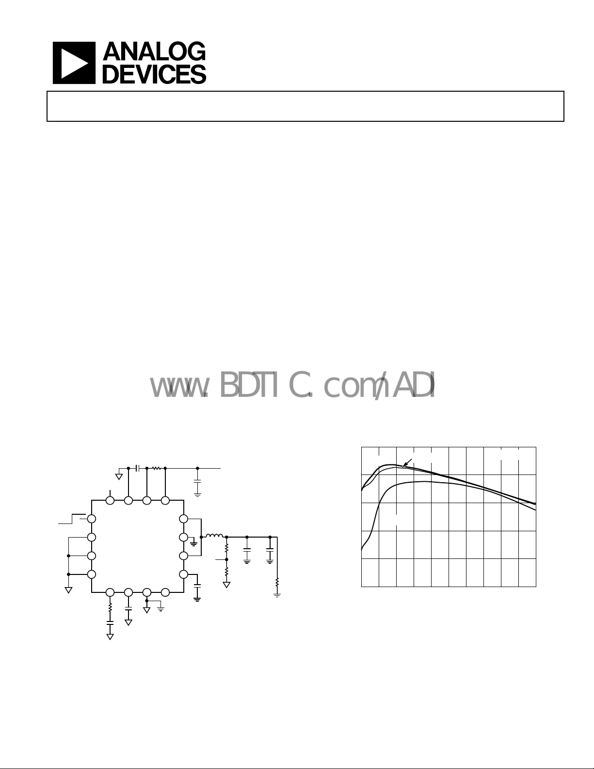
Figure 1. Circuit Configuration of ADP2107 with V
GND
EN
GND
ADP2107-ADJ
GND
GND
SS
COMP
5 6 7 8
70k
0.1
1nF
IN
AGND
IN
VININPUT VOLTAGE = 2.7V TO 5.5V
10
10F
OUTPUT VO LTAGE = 2.5V
12
LX2
2H
11
PGND
85k
10
LX1
PWIN2
NC
FB
V
IN
40k
9
10F
NC = NO CONNECT
10F
OUT
= 2.5 V
4.7F
LOAD
0A TO 2A
Step-Down DC-to-DC Converters
ADP2105/ADP2106/ADP2107
GENERAL DESCRIPTION
The ADP2105/ADP2106/ADP2107 are low quiescent current,
synchronous, step-down dc-to-dc converters in a compact 4 mm ×
4 mm LFCSP_VQ package. At medium to high load currents,
these devices use a current mode, constant frequency pulsewidth modulation (PWM) control scheme for excellent stability
and transient response. To ensure the longest battery life in portable
applications, the ADP2105/ADP2106/ADP2107 use a pulse
frequency modulation (PFM) control scheme under light load
conditions that reduces switching frequency to save power.
The ADP2105/ADP2106/ADP2107 run from input voltages of
2.7 V to 5.5 V, allowing single Li+/Li− polymer cell, multiple
alkaline/NiMH cells, PCMCIA, and other standard power sources.
The output voltage of ADP2105/ADP2106/ADP2107 is adjustable
from 0.8 V to the input voltage (indicated by ADJ), whereas the
ADP2105/ADP2106/ADP2107 are available in preset output
voltage options of 3.3 V, 1.8 V, 1.5 V, and 1.2 V (indicated by x.x V).
Each of these variations is available in three maximum current
levels: 1 A (ADP2105), 1.5 A (ADP2106), and 2 A (ADP2107). The
power switch and synchronous rectifier are integrated for minimal
external part count and high efficiency. During logic controlled
shutdown, the input is disconnected from the output, and it
draws less than 0.1 µA from the input source. Other key features
include undervoltage lockout to prevent deep battery discharge
and programmable soft start to limit inrush current at startup.
100
VIN = 3.3V
95
90
VIN = 5V
85
EFFICIENCY (%)
80
75
02
200 400 600 800 1000 1200 1400 1600 1800
VIN = 3.6V
LOAD CURRENT (mA)
Figure 2. Efficiency vs. Load Current for the ADP2107 with V
06079-002
V
OUT
= 2.5V
06079-001
000
= 2.5 V
OUT
Rev. C
Information furnished by Analog Devices is believed to be accurate and reliable. However, no
responsibility is assumed by Analog Devices for its use, nor for any infringements of patents or other
rights of third parties that may result from its use. Specifications subject to change without notice. No
license is granted by implication or otherwise under any patent or patent rights of Analog Devices.
Trademarks and registered trademarks are the property of their respective owners.
One Technology Way, P.O. Box 9106, Norwood, MA 02062-9106, U.S.A.
Tel: 781.329.4700 www.analog.com
Fax: 781.461.3113 ©2006–2008 Analog Devices, Inc. All rights reserved.

ADP2105/ADP2106/ADP2107
www.BDTIC.com/ADI
TABLE OF CONTENTS
Features .............................................................................................. 1
Applications ....................................................................................... 1
General Description ......................................................................... 1
Typical Operating Circuit ................................................................ 1
Revision History ............................................................................... 2
Functional Block Diagram .............................................................. 3
Specifications ..................................................................................... 4
Absolute Maximum Ratings ............................................................ 6
Thermal Resistance ...................................................................... 6
Boundary Condition .................................................................... 6
ESD Caution .................................................................................. 6
Pin Configuration and Function Descriptions ............................. 7
Typical Performance Characteristics ............................................. 8
Theory of Operation ...................................................................... 14
Control Scheme .......................................................................... 14
PWM Mode Operation .............................................................. 14
PFM Mode Operation ................................................................ 14
Pulse-Skipping Threshold ......................................................... 14
100% Duty Cycle Operation (LDO Mode) ............................. 14
Slope Compensation .................................................................. 15
Design Features ........................................................................... 15
Applications Information .............................................................. 16
REVISION HISTORY
9/08—Rev. B to Rev. C
Changes to Table Summary Statement .......................................... 4
Changes to LX Minimum On-Time Parameter, Table 1 ............. 5
7/08—Rev. A to Rev. B
Changes to General Description Section ...................................... 1
Changes to Figure 3 .......................................................................... 3
Changes to Table 1 ............................................................................ 4
Changes to Table 2 ............................................................................ 6
Changes to Figure 4 .......................................................................... 7
Changes to Table 4 ............................................................................ 7
Changes to Figure 26 ...................................................................... 11
Changes to Figure 31 Through Figure 34 .................................... 12
Changes to Figure 35 ...................................................................... 13
Changes to PMW Mode Operation Section and Pulse Skipping
Threshold Section ........................................................................... 14
Changes to Slope Compensation Section .................................... 15
Changes to Setting the Output Voltage Section ........................ 16
Changes to Figure 37 ...................................................................... 16
External Component Selection ................................................ 16
Setting the Output Voltage ........................................................ 16
Inductor Selection ...................................................................... 17
Output Capacitor Selection ....................................................... 18
Input Capacitor Selection .......................................................... 18
Input Filter ................................................................................... 19
Soft Start Period .......................................................................... 19
Loop Compensation .................................................................. 19
Bode Plots .................................................................................... 20
Load Transient Response .......................................................... 21
Efficiency Considerations ......................................................... 22
Thermal Considerations ............................................................ 22
Design Example .............................................................................. 24
External Component Recommendations .................................... 25
Circuit Board Layout Recommendations ................................... 27
Evaluation Board ............................................................................ 28
Evaluation Board Schematic for ADP2107 (1.8 V) ............... 28
Recommended PCB Board Layout (Evaluation Board Layout)
....................................................................................................... 28
Application Circuits ....................................................................... 30
Outline Dimensions ....................................................................... 33
Ordering Guide .......................................................................... 33
Changes to Inductor Selection Section ........................................ 17
Changes to Input Capacitor Selection Section ........................... 18
Changes to Figure 47 through Figure 52 ..................................... 21
Changes to Transition Losses Section and Thermal
Considerations Section .................................................................. 22
Changes to Table 11 ....................................................................... 25
Changes to Circuit Board Layout Recommendations Section..27
Changes to Table 12 ....................................................................... 26
Changes to Figure 53 ...................................................................... 28
Changes to Figure 56 Through Figure 57.................................... 30
Changes to Figure 58 Through Figure 59.................................... 31
Changes to Outline Dimensions .................................................. 33
3/07—Rev. 0 to Rev. A
Updated Format .................................................................. Universal
Changes to Output Characteristics and
LX (Switch Node) Characteristics Sections ................................... 3
Changes to Typical Performance Characteristics Section ........... 7
Changes to Load Transient Response Section ............................ 21
7/06—Revision 0: Initial Version
Rev. C | Page 2 of 36
ADP2105/ADP2106/ADP2107
www.BDTIC.com/ADI
FUNCTIONAL BLOCK DIAGRAM
COMP
SS
FB
FB
AGND
GND
GND
GND
NC
GND
EN
5
SOFT
6
START
16
16
7
FOR PRESET
VOLTAGE
OPTIONS ONLY
2
3
4
8
15
1
REFERENCE
SLOPE
COMPENSATION
OSCILLATOR
0.8V
GM ERROR
AMP
PWM/
PFM
CONTROL
CURRENT SENSE
AMPLI FIER
CURRENT
LIMIT
DRIVER
AND
ANTI-
SHOOT
THROUGH
ZERO CROSS
COMPARATOR
THERMAL
SHUTDOWN
14
9
13
10
12
11
IN
PWIN2
PWIN1
LX1
LX2
PGND
06079-037
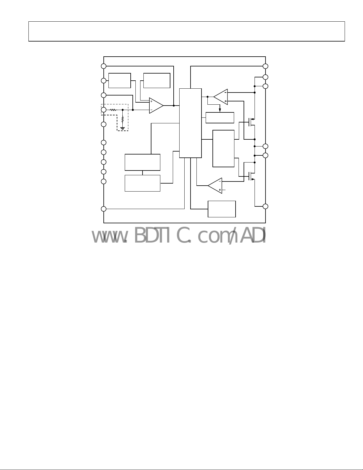
Figure 3.
Rev. C | Page 3 of 36

ADP2105/ADP2106/ADP2107
www.BDTIC.com/ADI
SPECIFICATIONS
VIN = 3.6 V @ TA = 25°C, unless otherwise noted.1
Table 1.
Parameter Min Typ Max Unit Conditions
INPUT CHARACTERISTICS
Input Voltage Range 2.7 5.5 V −40°C ≤ TJ ≤ +125°C
Undervoltage Lockout Threshold 2.4 V VIN rising
2.2 2.6 V VIN rising, −40°C ≤ TJ ≤ +125°C
2.2 V VIN falling
2.0 2.5 V VIN falling, −40°C ≤ TJ ≤ +125°C
Undervoltage Lockout Hysteresis
OUTPUT CHARACTERISTICS
Output Regulation Voltage 3.267 3.3 3.333 V 3.3 V, load = 10 mA
3.3 V 3.3 V, VIN = 3.6 V to 5.5 V, no load to full load
3.201 3.399 V
1.782 1.8 1.818 V 1.8 V, load = 10 mA
1.8 V 1.8 V, VIN = 2.7 V to 5.5 V, no load to full load
1.746 1.854 V
1.485 1.5 1.515 V 1.5, load = 10 mA
1.5 V ADP210x-1.5 V, VIN = 2.7 V to 5.5 V, no load to full load
1.455 1.545 V
1.188 1.2 1.212 V 1.2 V, load = 10 mA
1.2 V 1.2 V, VIN = 2.7 V to 5.5 V, no load to full load
1.164 1.236 V
Load Regulation 0.4 %/A ADP2105
0.5 %/A ADP2106
0.6 %/A ADP2107
Line Regulation
3
0.1 0.33 %/V ADP2105, measured in servo loop
0.1 0.3 %/V ADP2106 and ADP2107, measured in servo loop
Output Voltage Range 0.8 VIN V ADJ
FEEDBACK CHARACTERISTICS
FB Regulation Voltage 0.8 V ADJ
0.784 0.816 V ADJ, −40°C ≤ TJ ≤ +125°C
FB Bias Current −0.1 +0.1 µA ADJ, −40°C ≤ TJ ≤ +125°C
20 µA 3.3 V output voltage, −40°C ≤ TJ ≤ +125°C
2
200 mV V
3 µA 1.2 V output voltage
6 µA 1.2 V output voltage, −40°C ≤ TJ ≤ +125°C
4 µA 1.5 V output voltage
8 µA 1.5 V output voltage, −40°C ≤ TJ ≤ +125°C
5 µA 1.8 V output voltage
10 µA 1.8 V output voltage, −40°C ≤ TJ ≤ +125°C
10 µA 3.3 V output voltage
falling
IN
3.3 V, V
−40°C ≤ T
1.8 V, V
−40°C ≤ T
= 3.6 V to 5.5 V, no load to full load,
IN
≤ +125°C
J
= 2.7 V to 5.5 V, no load to full load,
IN
≤ +125°C
J
ADP210x-1.5 V, V
−40°C ≤ T
1.2 V, V
−40°C ≤ T
≤ +125°C
J
= 2.7 V to 5.5 V, no load to full load,
IN
≤ +125°C
J
= 2.7 V to 5.5 V, no load to full load,
IN
Rev. C | Page 4 of 36

ADP2105/ADP2106/ADP2107
www.BDTIC.com/ADI
Parameter Min Typ Max Unit Conditions
INPUT CURRENT CHARACTERISTICS
IN Operating Current 20 µA ADP210x(ADJ), VFB = 0.9 V
30 µA ADP210x(ADJ), VFB = 0.9 V, −40°C ≤ TJ ≤ +125°C
20 µA
30 µA
IN Shutdown Current
4
0.1 1 µA V
LX (SWITCH) NODE CHARACTERISTICS
LX On Resistance
4
190 mΩ P-channel switch, ADP2105
270 mΩ P-channel switch, ADP2105, −40°C ≤ TJ ≤ +125°C
100 mΩ P-channel switch, ADP2106 and ADP2107
165 mΩ
160 mΩ N-channel synchronous rectifier, ADP2105
230 mΩ
90 mΩ N-channel synchronous rectifier, ADP2106 and ADP2107
140 mΩ
LX Leakage Current
LX Peak Current Limit
4, 5
0.1 1 µA V
5
2.9 A P-channel switch, ADP2107
2.6 3.3 A P-channel switch, ADP2107, −40°C ≤ TJ ≤ +125°C
2.25 A P-channel switch, ADP2106
2.0 2.6 A P-channel switch, ADP2106, −40°C ≤ TJ ≤ +125°C
1.5 A P-channel switch, ADP2105
1.3 1.8 A P-channel switch, ADP2105, −40°C ≤ TJ ≤ +125°C
LX Minimum On-Time 110 ns In PWM mode of operation, −40°C ≤ TJ ≤ +125°C
ENABLE CHARACTERISTICS
EN Input High Voltage 2 V VIN = 2.7 V to 5.5 V, −40°C ≤ TJ ≤ +125°C
EN Input Low Voltage 0.4 V VIN = 2.7 V to 5.5 V, −40°C ≤ TJ ≤ +125°C
EN Input Leakage Current −0.1 µA VIN = 5.5 V, VEN = 0 V, 5.5 V
−1 +1 µA VIN = 5.5 V, VEN = 0 V, 5.5 V, −40°C ≤ TJ ≤ +125°C
OSCILLATOR FREQUENCY 1.2 MHz VIN = 2.7 V to 5.5 V
1 1.4 MHz VIN = 2.7 V to 5.5 V, −40°C ≤ TJ ≤ +125°C
SOFT START PERIOD 750 1000 1200 µs CSS = 1 nF
THERMAL CHARACTERISTICS
Thermal Shutdown Threshold 140
Thermal Shutdown Hysteresis 40
COMPENSATOR
TRANSCONDUCTANCE (g
)
m
CURRENT SENSE AMPLIFIER GAIN (GCS)
50 µA/V
2
1.875 A/V ADP2105
°C
°C
2.8125 A/V ADP2106
3.625 A/V ADP2107
1
All limits at temperature extremes are guaranteed via correlation using standard statistical quality control (SQC). Typical values are at TA = 25°C.
2
Guaranteed by design.
3
The ADP2105/ADP2106/ADP2107 line regulation was measured in a servo loop on the automated test equipment that adjusts the feedback voltage to achieve a
specific COMP voltage.
4
All LX (switch) node characteristics are guaranteed only when the LX1 pin and LX2 pin are tied together.
5
These specifications are guaranteed from −40°C to +85°C.
ADP210x(x.x V) output voltage 10% above regulation
voltage
ADP210x(x.x V) output voltage 10% above regulation
voltage, −40°C ≤ TJ ≤ +125°C
= 0 V
EN
P-channel switch, ADP2106 and ADP2107,
−40°C ≤ TJ ≤ +125°C
N-channel synchronous rectifier, ADP2105,
−40°C ≤ T
≤ +125°C
J
N-channel synchronous rectifier, ADP2106 and ADP2107,
−40°C ≤ T
IN
≤ +125°C
J
= 5.5 V, VLX = 0 V, 5.5 V
Rev. C | Page 5 of 36
ADP2105/ADP2106/ADP2107
www.BDTIC.com/ADI
ABSOLUTE MAXIMUM RATINGS
Table 2.
Parameter Rating
IN, EN, SS, COMP, FB to AGND −0.3 V to +6 V
LX1, LX2 to PGND −0.3 V to (VIN + 0.3 V)
PWIN1, PWIN2 to PGND −0.3 V to +6 V
PGND to AGND −0.3 V to +0.3 V
GND to AGND −0.3 V to +0.3 V
PWIN1, PWIN2 to IN −0.3 V to +0.3 V
Operating Junction Temperature Range −40°C to +125°C
Storage Temperature Range −65°C to +150°C
Soldering Conditions JEDEC J-STD-020
Stresses above those listed under Absolute Maximum Ratings
may cause permanent damage to the device. This is a stress
rating only; functional operation of the device at these or any
other conditions above those indicated in the operational
section of this specification is not implied. Exposure to absolute
maximum rating conditions for extended periods may affect
device reliability.
THERMAL RESISTANCE
θJA is specified for the worst-case conditions, that is, a device
soldered in a circuit board for surface-mount packages.
Table 3. Thermal Resistance
Package Type θ
16-Lead LFCSP_VQ/QFN 40 °C/W
Maximum Power Dissipation 1 W
BOUNDARY CONDITION
Natural convection, 4-layer board, exposed pad soldered to the PCB.
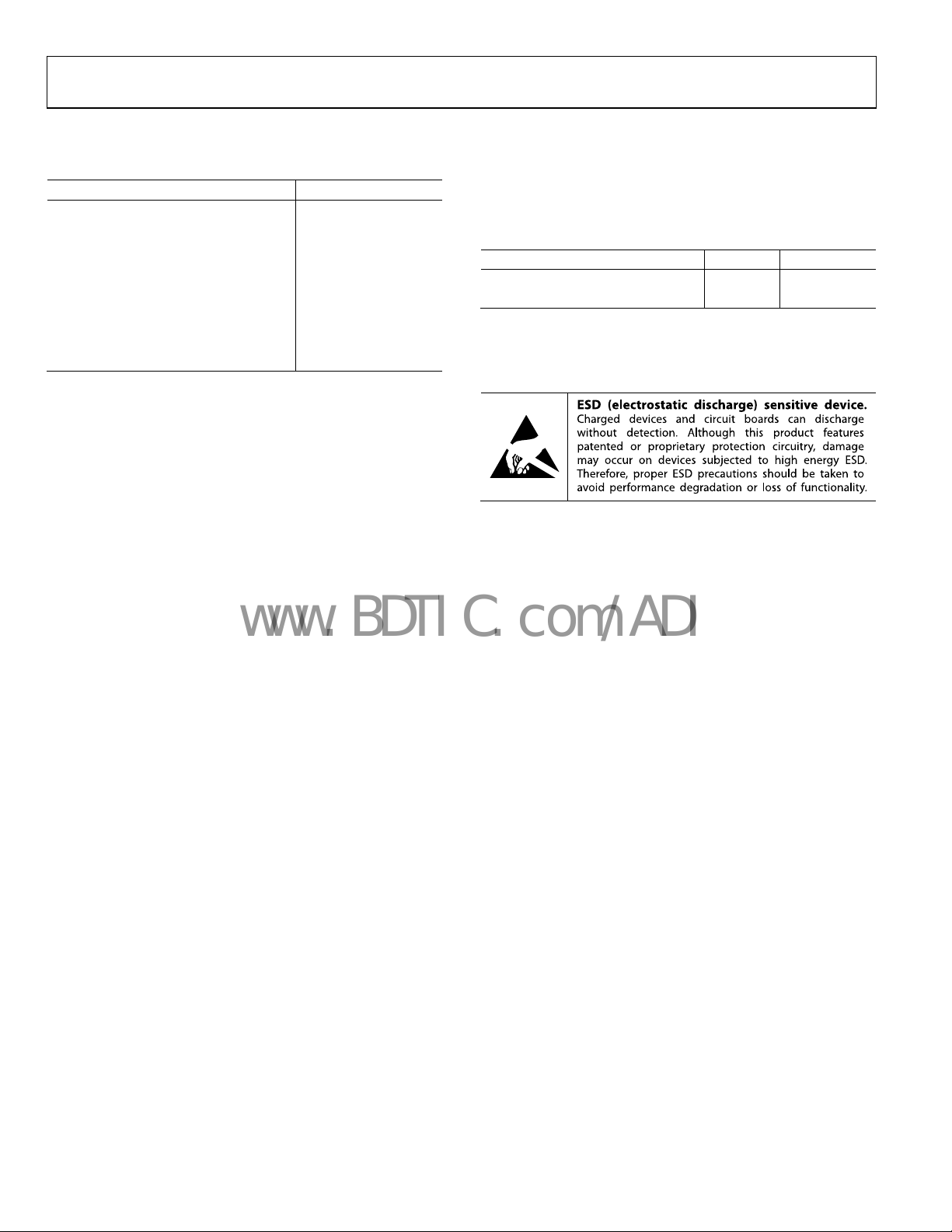
ESD CAUTION
JA
Unit
Rev. C | Page 6 of 36

ADP2105/ADP2106/ADP2107
www.BDTIC.com/ADI
PIN CONFIGURATION AND FUNCTION DESCRIPTIONS
15 GND
16 FB
14 IN
13 PWIN1
PIN 1
EN 1
GND 2
GND 3
GND 4
INDICATO R
ADP2105/
ADP2106/
ADP2107
TOP VIEW
(Not to Scale)
6
SS
AGND 7
COMP 5
NC = NO CONNECT
Figure 4. Pin Configuration
Table 4. Pin Function Descriptions
Pin No. Mnemonic Description
1 EN
Enable Input. Drive EN high to turn on the device. Drive EN low to turn off the device and reduce the input
current to 0.1 µA.
2, 3, 4, 15 GND
Test Pins. These pins are used for internal testing and are not ground return pins. These pins are to be tied to the
AGND plane as close as possible to the ADP2105/ADP2106/ADP2107.
5 COMP
Feedback Loop Compensation Node. COMP is the output of the internal transconductance error amplifier. Place
a series RC network from COMP to AGND to compensate the converter. See the Loop Compensation section.
6 SS
Soft Start Input. Place a capacitor from SS to AGND to set the soft start period. A 1 nF capacitor sets a 1 ms soft
start period.
7 AGND
Analog Ground. Connect the ground of the compensation components, the soft start capacitor, and the voltage
divider on the FB pin to the AGND pin as close as possible to the ADP2105/ ADP2106/ADP2107. The AGND is
also to be connected to the exposed pad of ADP2105/ADP2106/ADP2107.
8 NC No Connect. This is not internally connected and can be connected to other pins or left unconnected.
9, 13
PWIN2,
PWIN1
Power Source Inputs. The source of the PFET high-side switch. Bypass each PWIN pin to the nearest PGND plane with a
4.7 µF or greater capacitor as close as possible to the ADP2105/ADP2106/ ADP2107. See the Input Capacitor
Selection section.
10, 12 LX1, LX2
Switch Outputs. The drain of the P-channel power switch and N-channel synchronous rectifier. These pins are to
be tied together and connected to the output LC filter between LX and the output voltage.
11 PGND
Power Ground. Connect the ground return of all input and output capacitors to the PGND pin using a power
ground plane as close as possible to the ADP2105/ADP2106/ADP2107. The PGND is then to be connected to the
exposed pad of the ADP2105/ADP2106/ADP2107.
14 IN
Power Input. The power source for the ADP2105/ADP2106/ADP2107 internal circuitry. Connect IN and PWIN1
with a 10 Ω resistor as close as possible to the ADP2105/ADP2106/ADP2107. Bypass IN to AGND with a 0.1 µF or
greater capacitor. See the Input Filter section.
16 FB
Output Voltage Sense or Feedback Input. For fixed output versions, connect to the output voltage. For
adjustable versions, FB is the input to the error amplifier. Drive FB through a resistive voltage divider to set the
output voltage. The FB regulation voltage is 0.8 V.
12 LX2
11 PGND
10 LX1
9 PWIN2
NC 8
06079-003
Rev. C | Page 7 of 36
ADP2105/ADP2106/ADP2107
www.BDTIC.com/ADI
TYPICAL PERFORMANCE CHARACTERISTICS
100
100
95
90
85
80
75
EFFICIENCY (%)
70
65
60
11
VIN = 2.7V
VIN = 5.5V
VIN = 3.6V
VIN = 4.2V
INDUCTOR: SD14, 2.5µH
DCR: 60m
T
= 25°C
A
10 100
LOAD CURRENT (mA)
06079-084
000
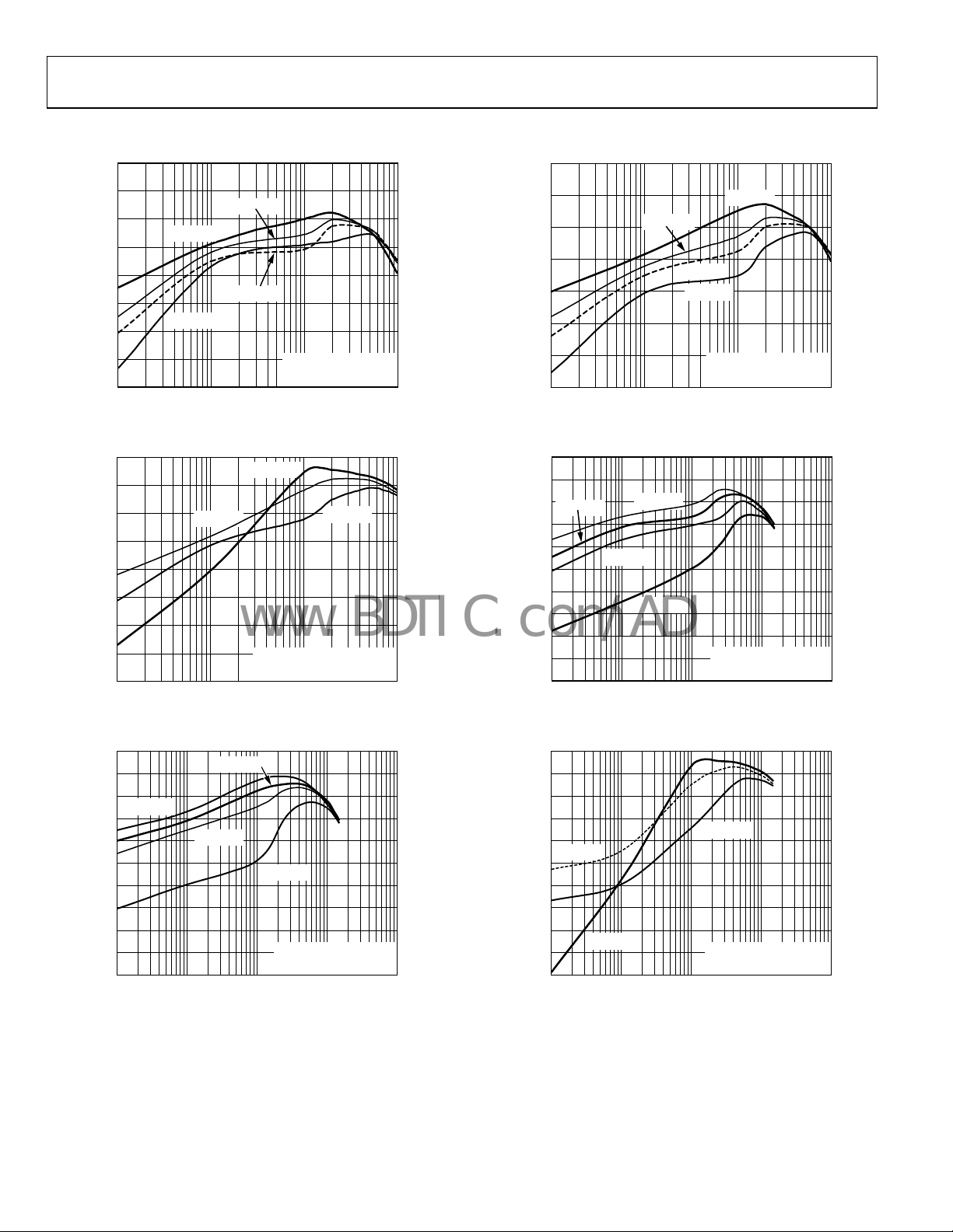
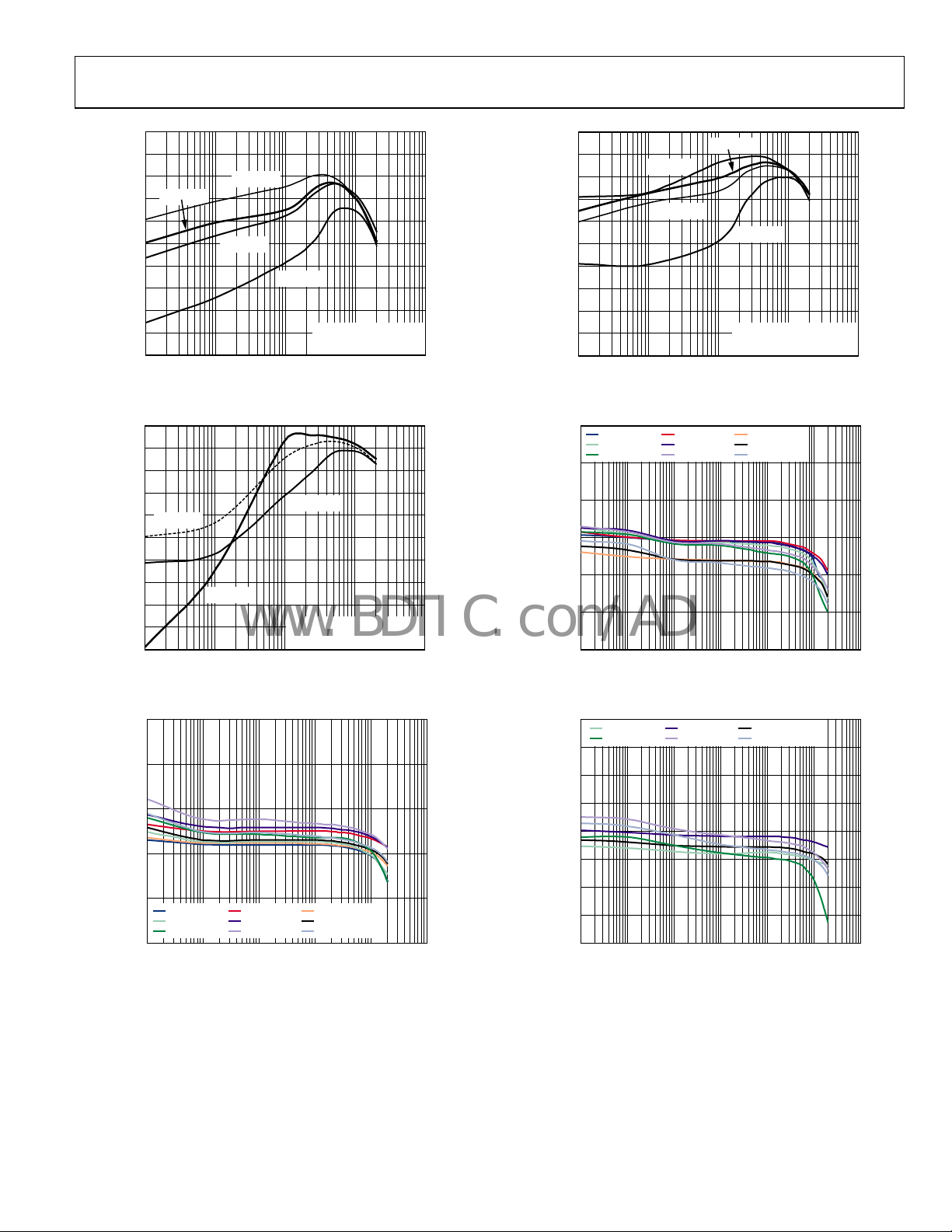
Figure 5. Efficiency—ADP2105 (1.2 V Output)
100
95
90
85
80
75
EFFICIENCY (%)
70
65
60
1 1000
VIN = 4.2V
10 100
LOAD CURRENT (mA)
VIN = 3.6V
VIN = 5.5V
INDUCTOR: CDRH5D18, 4.1H
DCR: 43m
T
= 25°C
A
06079-085
Figure 6. Efficiency—ADP2105 (3.3 V Output)
100
95
90
VIN = 2.7V
85
80
75
70
EFFICIENCY (%)
65
60
55
50
1 10k
VIN = 3.6V
VIN = 4.2V
VIN = 5.5V
INDUCTOR: D62L CB, 2µH
DCR: 28m
T
= 25°C
A
10 100 1k
LOAD CURRENT (mA)
06079-062
Figure 7. Efficiency—ADP2106 (1.8 V Output)
95
90
85
80
EFFICIE NCY (%)
75
70
65
1 1000
Figure 8. Efficiency—ADP2105 (1.8 V Output)
100
95
90
VIN = 3.6V
85
80
75
70
EFFICIENCY (%)
65
60
55
50
1 10k
Figure 9. Efficiency—ADP2106 (1.2 V Output)
100
95
90
85
80
VIN = 4.2V
75
70
EFFICIENCY (%)
65
60
55
50
VIN = 3.6V
1 10k
Figure 10. Efficiency—ADP2106 (3.3 V Output)
VIN = 2.7V
VIN = 3.6V
VIN = 4.2V
VIN = 5.5V
INDUCTOR: SD3814, 3.3µH
DCR: 93m
T
= 25°C
A
10 100
LOAD CURRENT (mA)
VIN = 2.7V
VIN = 4.2V
VIN = 5.5V
INDUCTOR: D62L CB, 2µH
DCR: 28m
T
= 25°C
A
10 100 1k
LOAD CURRENT (mA)
VIN = 5.5V
INDUCTOR: D62L CB, 3.3µH
DCR: 47m
T
= 25°C
A
10 100 1k
LOAD CURRENT (mA)
06079-086
06079-008
06079-053
Rev. C | Page 8 of 36
ADP2105/ADP2106/ADP2107
www.BDTIC.com/ADI
100
95
90
VIN = 3.6V
85
80
75
70
EFFICIENCY (%)
65
60
55
50
1 10k
VIN = 2.7V
VIN = 4.2V
VIN = 5.5V
INDUCTOR: SD12, 1.2µH
DCR: 37m
T
= 25°C
A
10 100 1k
LOAD CURRENT (mA)
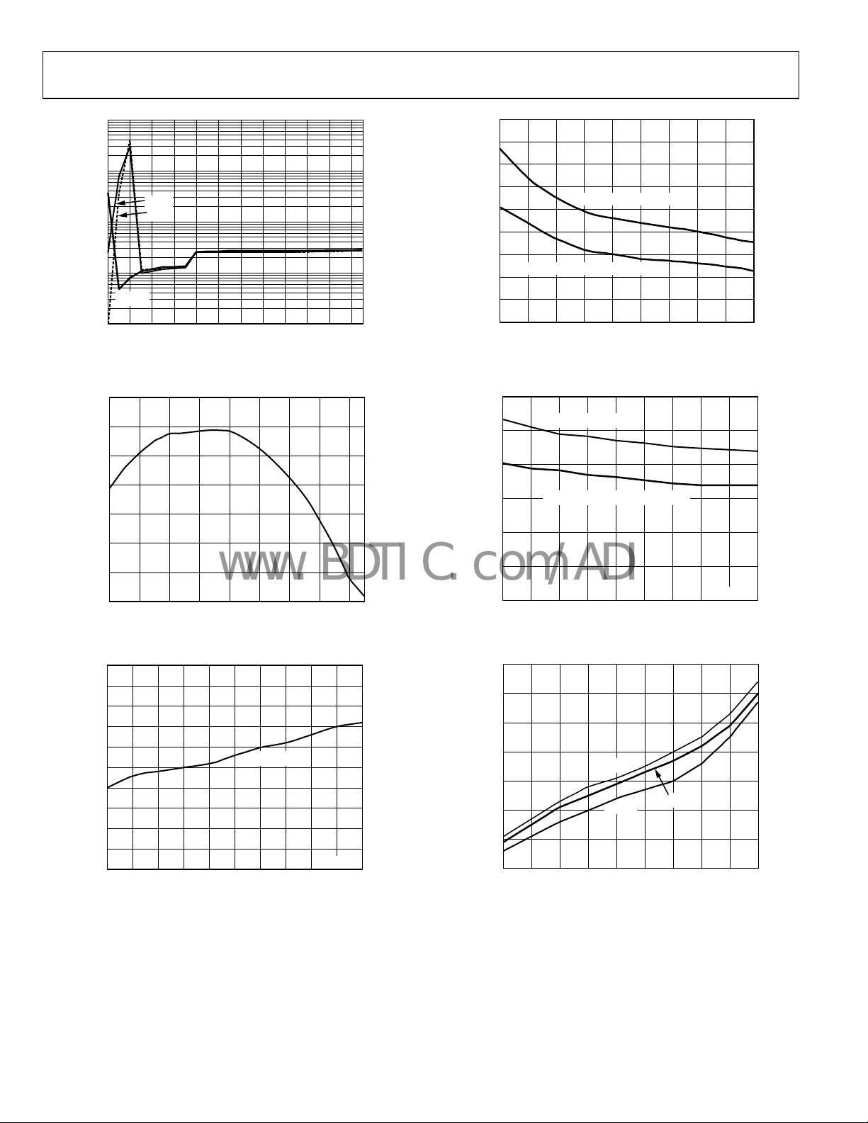
Figure 11. Efficiency—ADP2107 (1.2 V)
100
95
90
85
80
VIN = 4.2V
75
70
EFFICIENCY (%)
65
60
55
50
1 10k
VIN = 3.6V
10 100 1k
LOAD CURRENT (mA)
VIN = 5.5V
INDUCTOR: CDRH5D28, 2. 5µH
DCR: 13m
T
= 25°C
A
Figure 12. Efficiency—ADP2107 (3.3 V)
1.85
1.83
06079-010
06079-054
100
95
90
85
80
75
70
EFFICIENCY (%)
65
60
55
50
1 10k
VIN = 2.7V
VIN = 4.2V
10 100 1k
VIN = 3.6V
VIN = 5.5V
INDUCTOR: D62L CB, 1.5µH
DCR: 21m
T
= 25°C
A
LOAD CURRENT (mA)
Figure 14. Efficiency—ADP2107 (1.8 V)
1.23
2.7V, –40° C 2.7V, +25°C 2. 7V, +125°C
3.6V, –40° C 3.6V, +25°C 3. 6V, +125°C
5.5V, –40° C 5.5V, +25°C
1.22
1.21
1.20
1.19
OUTPUT VOLTAGE (V)
1.18
1.17
0.01 10k
0.1 1 10 100 1k
LOAD CURRENT (mA)
5.5V, +125° C
Figure 15. Output Voltage Accuracy—ADP2107 (1.2 V)
3.38
3.6V, –40°C 3.6V, +25°C 3.6V, +125° C
5.5V, –40°C 5.5V, +25°C
3.36
3.34
5.5V, +125° C
06079-063
06079-082
1.81
1.79
OUTPUT VOLTAGE (V)
1.77
2.7V, –40°C 2.7V, +25°C 2.7V, +125° C
3.6V, –40°C 3.6V, +25°C 3.6V, +125° C
5.5V, –40°C 5.5V, +25°C
1.75
0.1 10k
1 10 100 1k
LOAD CURRENT (mA)
5.5V, +125° C
06079-064
Figure 13. Output Voltage Accuracy—ADP2107 (1.8 V)
Rev. C | Page 9 of 36
3.32
3.30
3.28
OUTPUT VOLTAGE (V)
3.26
3.24
3.22
0.01 10k
0.1 1 10 100 1k
LOAD CURRENT (mA)
Figure 16. Output Voltage Accuracy—ADP2107 (3.3 V)
06079-081
ADP2105/ADP2106/ADP2107
www.BDTIC.com/ADI
10k
1k
+25°C
–40°C
+125°C
1.2 1.6 2. 0 2.4 2. 8 3.2 3.6 4.0 4.4 4.8 5.2
INPUT VOLTAG E (V)
Figure 17. Quiescent Current vs. Input Voltage
QUIESCENT CURRENT (µA)
100
0.802
0.801
10
1
0.8
190
180
170
160
150
140
130
NMOS SYNCHRONOUS RECTIFI ER
120
SWITCH ON RESISTANCE (m)
110
06079-016
100
2.7 3.0 3.3 3.6 3.9 4.2 4.5 5.1 5.44.8
PMOS POWER SWITCH
INPUT VOLTAGE (V)
06079-093
Figure 20. Switch On Resistance vs. Input Voltage—ADP2105
120
100
PMOS POWER SWITCH
0.800
0.799
0.798
0.797
FEEDBACK VOLT AGE (V)
0.796
0.795
–40 125
–20 0 20 40 60 80 100 120
TEMPERATURE ( °C)
Figure 18. Feedback Voltage vs. Temperature
1.75
1.70
1.65
1.60
1.55
1.50
1.45
1.40
PEAK CURRENT LIMIT (A)
1.35
1.30
1.25
2.7 5.7
3.0 3.3 3.6 3.9 4.2 4.5 4.8 5.1 5.4
INPUT VOLTAGE (V)
ADP2105 (1A)
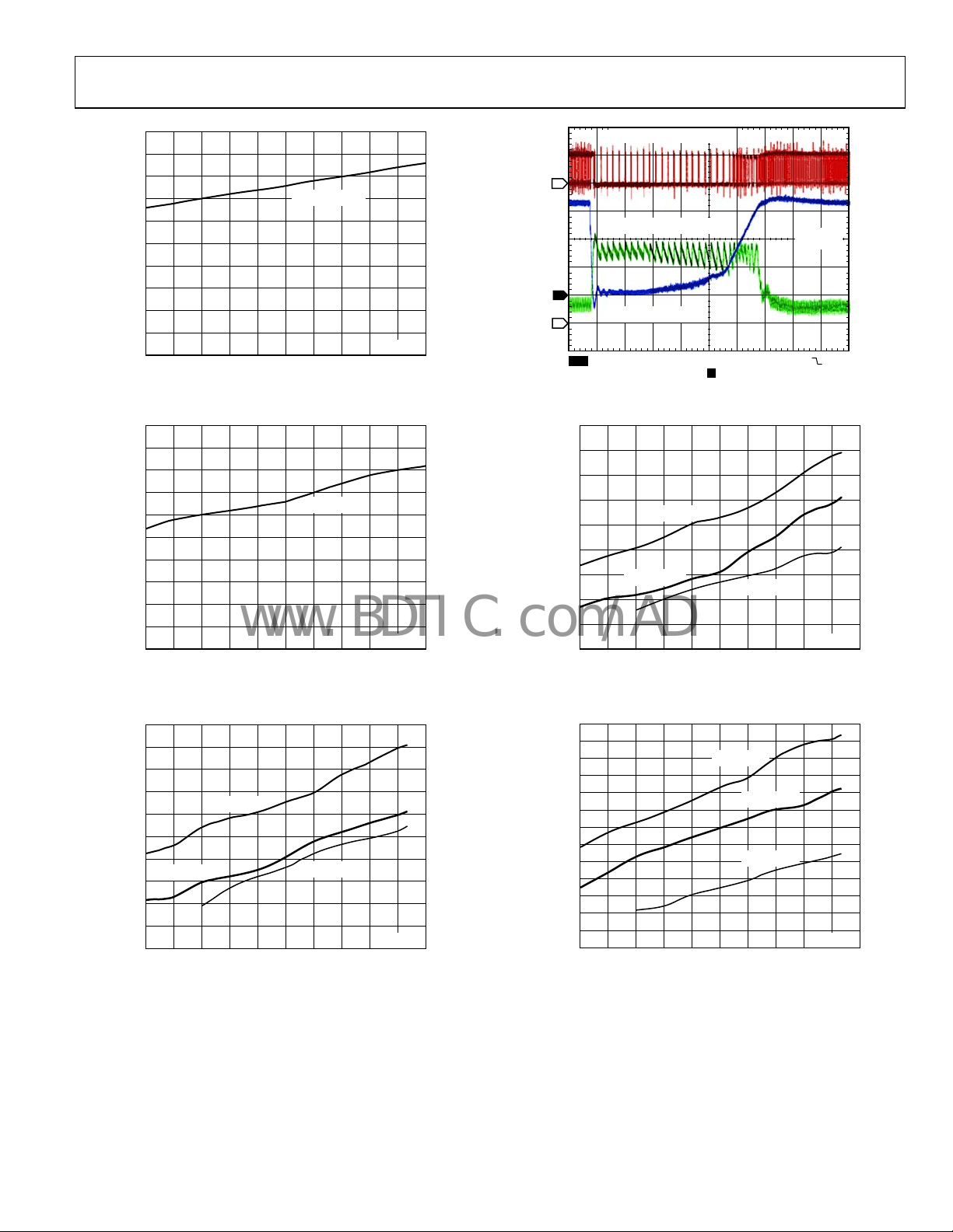
Figure 19. Peak Current Limit of ADP2105
TA = 25°C
80
60
40
SWITCH ON RESISTANCE (m)
20
06079-017
0
2.7 5.4
NMOS SYNCHRONOUS RECTIFIER
TA = 25°C
3.0 3.3 3.6 3.9 4.2 4.5 4. 8 5.1
INPUT VOLTAGE (V)
06079-018
Figure 21. Switch On Resistance vs. Input Voltage—ADP2106 and ADP2107
1260
1250
1240
1230
1220
1210
SWITCHING FREQUENCY ( kHz)
1200
06079-073
1190
2.7 5.4
3.0 3.3 3.6 3.9 4.2 4.5 4. 8 5.1
+125°C
–40°C
INPUT VOLTAG E (V)
+25°C
06079-021
Figure 22. Switching Frequency vs. Input Voltage
Rev. C | Page 10 of 36
ADP2105/ADP2106/ADP2107
www.BDTIC.com/ADI
2.35
2.30
2.25
2.20
2.15
2.10
2.05
2.00
PEAK CURRENT LIMIT (A)
1.95
1.90
1.85
2.7 5.7
3.0 3.3 3.6 3.9 4.2 4.5 4.8 5.1 5.4
INPUT VOLTAGE (V)
ADP2106 (1.5A)
TA = 25°C
Figure 23. Peak Current Limit of ADP2106
3.00
2.95
2.90
2.85
2.80
2.75
2.70
2.65
PEAK CURRENT LIMIT (A)
2.60
2.55
2.50
2.7 5.7
3.0 3.3 3.6 3.9 4.2 4.5 4.8 5.1 5.4
INPUT VOLTAGE (V)
ADP2107 (2A)
TA = 25°C
Figure 24. Peak Current Limit of ADP2107
150
135
120
105
90
75
60
V
45
30
15
PULSE-SKIP PING THRESHO LD CURRENT (mA)
0
2.7 5.7
V
= 1.2V
OUT
V
= 2.5V
= 1.8V
OUT
3.0 3.3 3.6 3.9 4.2 4.5 4.8 5.1 5.4
INPUT VOLTAGE (V)
OUT
TA = 25°C
Figure 25. Pulse-Skipping Threshold vs. Input Voltage for ADP2106
3
1
4
06079-072
135
120
105
90
75
60
45
30
15
06079-071
PULSE-SKIP PING THRESHO LD CURRENT (mA)
Figure 27. Pulse-Skipping Threshold vs. Input Voltage for ADP2105
195
180
165
150
135
120
105
90
75
60
45
30
15
06079-067
PULSE-SKIP PING THRESHO LD CURRENT (mA)
Figure 28. Pulse-Skipping Threshold vs. Input Voltage for ADP2107
LX (SWITCH) NODE
CH1 1V
INDUCTOR CURRENT
OUTPUT VOLTAGE
M 10µs A CH1 1.78V
45.8%CH4 1ACH3 5V
T
: 260mV
@: 3.26V
Figure 26. Short -Circuit Response at Output
V
= 1.2V
OUT
V
= 1.8V
OUT
0
2.7 5.7
3.0 3.3 3.6 3.9 4.2 4.5 4.8 5.1 5.4
INPUT VOLTAGE (V)
0
2.7 5.7
3.0 3.3 3.6 3.9 4.2 4.5 4.8 5.1 5.4
INPUT VOLTAGE (V)
V
= 2.5V
OUT
TA = 25°C
V
= 1.2V
OUT
V
= 1.8V
OUT
V
= 2.5V
OUT
TA = 25°C
06079-074
06079-066
06079-068
Rev. C | Page 11 of 36
 Loading...