Low Duty Cycle, 600 mA, 3 MHz Synchronous
www.BDTIC.com/ADI
FEATURES
Input voltage range: 2.7 V to 5.5 V
600 mA maximum load current
95% efficiency
Low duty cycle operation
Only 3 tiny external ceramic components
3 MHz typical operating frequency
Fixed output voltage from 0.8 V to 1.875 V
Adjustable output voltage up to 3.3 V
0.01 μA shutdown supply current
Automatic power save mode
Internal synchronous rectifier
Internal soft start
Internal compensation
Enable/shutdown logic input
Undervoltage lockout
Current limit protection
Thermal shutdown
Small 8-lead, 3 mm × 3 mm LFCSP package
APPLICATIONS
USB powered devices
WLAN and gateways
Point of loads
Processor core power from 5 V
Digital cameras
PDAs and palmtop computers
Portable media players, GPS
Step-Down DC-to-DC Converter
ADP2102
GENERAL DESCRIPTION
The ADP2102 is a synchronous step-down dc-to-dc converter
that converts a 2.7 V to 5.5 V unregulated input voltage to a lower
regulated output voltage with up to 95% efficiency and 1%
accuracy. The low duty cycle capability of the ADP2102 is ideal for
USB applications or 5 V systems that power up submicron subvolt
processor cores. Its 3 MHz typical operating frequency and excellent transient response allow the use of small, low cost 1 µH
inductors and 2.2 µF ceramic capacitors. At medium-to-high
load currents, it uses a current mode, pseudofixed frequency pulsewidth modulation to extend battery life. To ensure the longest
batter y life in portable applications, the ADP2102 has a power save
mode (PSM) that reduces the switching frequency under light
load conditions to significantly reduce quiescent current.
The ADP2102 is available in both fixed and adjustable output
v
oltage options with 600 mA maximum output current. The preset
output voltage options voltage are 1.875 V, 1.8 V, 1.5 V, 1.375 V,
1.25 V, 1.2 V, 1.0 V, and 0.8 V. The adjustable voltage option is
available from 0.8 V to 3.3 V. The ADP2102 requires only three
external components and consumes 0.01 µA in shutdown mode.
The ADP2102 is available in an 8-lead LFCSP package and is
s
pecified for the −40 °C to +85 °C temperature range.
TYPICAL PERFORMANCE CHARACTERISTICS
100
95
90
85
80
75
EFFICIENCY (%)
70
65
60
10 100 1000
Rev. B
Information furnished by Analog Devices is believed to be accurate and reliable. However, no
responsibility is assumed by Anal og Devices for its use, nor for any infringements of patents or ot her
rights of third parties that may result from its use. Specifications subject to change without notice. No
license is granted by implication or otherwise under any patent or patent rights of Analog Devices.
Trademarks and registered trademarks are the property of their respective owners.
VIN = 3.6V
VIN = 2.7V
VIN = 3V
VIN = 4.2V
LOAD CURRENT (mA)
Figure 1.
V
OUT
T
A
= 1.375V
= 25°C
06631-052
TYPICAL APPLICATIONS CIRCUIT
INPUT VOLTAGE
2.7V TO 5. 5V
2.2µF
FORCED
DCM/
CCM
One Technology Way, P.O. Box 9106, Norwood, MA 02062-9106, U.S.A.
Tel: 781.329.4700 www.analog.com
Fax: 781.461.3113 ©2007 Analog Devices, Inc. All rights reserved.
C
IN
CCM
V
IN
MODE
OFF
ADP2102
EN GND
ON
LX
FB/OUT
Figure 2.
OUTPUT VO LTAGE
L
0.8V TO 1. 875V
1µH
C
2.2µF
OUT
06631-001

ADP2102
www.BDTIC.com/ADI
TABLE OF CONTENTS
Features .............................................................................................. 1
Applications....................................................................................... 1
General Description......................................................................... 1
Typical Performance Characteristics ............................................. 1
Typical Applicat i o n s C i rc uit............................................................ 1
Revision History ............................................................................... 2
Specifications..................................................................................... 3
Absolute Maximum Ratings............................................................ 4
Thermal Resistance ...................................................................... 4
Boundary Condition .................................................................... 4
ESD Caution.................................................................................. 4
Pin Configuration and Function Descriptions............................. 5
Typical Performance Characteristics ............................................. 6
Theory of Operation ...................................................................... 13
Control Scheme .......................................................................... 13
Constant On-Time Timer......................................................... 13
Forced Continuous Conduction Mode ...................................13
Power Save Mode........................................................................ 13
Synchronous Rectification ........................................................14
Current Limit .............................................................................. 14
Soft Start...................................................................................... 15
Enable........................................................................................... 15
Undervoltage L ockout ............................................................... 15
Thermal Shutdown .................................................................... 15
Applications Information.............................................................. 16
Inductor Selection...................................................................... 16
Input Capacitor Selection.......................................................... 16
Output Capacitor Selection....................................................... 16
Typical Applicat i o n s C i rc uits .................................................... 17
Setting the Output Voltage........................................................ 19
Efficiency Considerations ......................................................... 19
Thermal Considerations............................................................ 20
Design Example.......................................................................... 20
Circuit Board Layout Recommendations ................................... 22
Recommended Layout............................................................... 22
Outline Dimensions ....................................................................... 24
Ordering Guide .......................................................................... 24
REVISION HISTORY
9/07—Rev. A to Rev. B
Changes to Features, Applications, and General Description .... 1
Changes to Table 4............................................................................ 5
Changes to Table 6.......................................................................... 17
Changes to Table 7.......................................................................... 19
Changes to Circuit Board Layout Recommendations Section.... 21
Updated Outline Dimensions....................................................... 23
Changes to Ordering Guide.......................................................... 23
6/07—Rev. 0 to Rev. A
Changes to Ordering Guide.......................................................... 23
6/07—Revision 0: Initial Version
Rev. B | Page 2 of 24

ADP2102
www.BDTIC.com/ADI
SPECIFICATIONS
VIN = 3.6 V, EN = VIN, MODE = VIN, TA = 25°C, unless otherwise noted. Bold values indicate −40°C ≤ TA ≤ +85°C.
Table 1.
Parameter Conditions Min Typ Max Unit
INPUT CHARACTERISTICS
Input Voltage Range
2
2.7 5.5 V
Undervoltage Lockout Threshold VIN rising 2.2 2.4 2.5 V
Undervoltage Lockout Hysteresis 220 mV
OUTPUT CHARACTERISTICS
Output Voltage Range ADP2102-xx 0.8 1.875 V
Output Voltage Range ADP2102-ADJ 0.8 3.3 V
Output Voltage Initial Accuracy ADP2102-xx, TA= 25°C, I
ADP2102-xx, −40°C ≤TA ≤ 85°C, I
Load Regulation V
= 0.8 V to 1.875 V, I
OUT
Line Regulation VIN = 2.7 V to 5.5 V, I
= 0 mA
LOAD
= 0 mA
LOAD
= 0 mA to 600 mA 0.5 %
LOAD
= 10 mA 0.3 %
LOAD
−1
−2
FEEDBACK CHARACTERISTICS
FB Regulation Voltage ADP2102-ADJ
784
800
FB Bias Current ADP2102-ADJ, ADP2102-0.8
FB Impedance ADP2102-xx 375 kΩ
CURRENT CHARACTERISTICS
Operating Current ADP2102 PSM mode, I
= 0 mA 70
LOAD
Shutdown Current EN = 0 V 0.01
Output Current ADP2102, VIN = 2.7 V to 5.5 V 600 mA
LX (SWITCH NODE) CHARACTERISTICS
LX On Resistance P-channel switch, ILX = 100 mA
N-channel synchronous rectifier, ILX = 100 mA
325
200
LX Leakage Current VIN = 5.5 V, VLX = 0 V, 5.5 V
LX Minimum Off-Time ADP2102-xx, ADP2102-ADJ 100 ns
LX On-Time ADP2102-0.8
ADP2102-1.0
ADP2102-1.2
ADP2102-1.25
ADP2102-1.375
ADP2102-1.5
ADP2102-1.8
ADP2102-1.875
ADP2102-ADJ-1.2
ADP2102-ADJ-1.5
ADP2102-ADJ-1.875
ADP2102-ADJ-3.3 (VIN = 5 V)
55
70
100
103
135
150
180
190
80
155
200
198
87
107
131
133
165
182
220
237
131
177
226
238
Valley Current Limit 1 A
ENABLE, MODE CHARACTERISTICS
EN, MODE Input High Threshold
1.3
V
EN, MODE Input Low Threshold
EN, MODE Input Leakage Current VIN = 5.5 V, EN = MODE = 0 V, 5.5 V
SOFT START PERIOD
250
500
THERMAL CHARACTERISTICS
Thermal Shutdown Threshold 150 °C
Thermal Shutdown Hysteresis 15 °C
1
All limits at temperature extremes are guaranteed via correlation using standard statistical quality control (SQC).
2
The input voltage (VIN) range over which the rest of the specifications are valid. The part operates as expected until VIN goes below the UVLO threshold.
1
+1
+2
816
50
99
1
600
400
1
105
135
160
169
195
210
260
270
170
210
275
270
0.4
1
800
%
%
mV
nA
µA
µA
mΩ
mΩ
µA
ns
ns
ns
ns
ns
ns
ns
ns
ns
ns
ns
ns
V
µA
µs
Rev. B | Page 3 of 24
ADP2102
www.BDTIC.com/ADI
ABSOLUTE MAXIMUM RATINGS
Table 2.
Parameter Rating
AVIN, EN, MODE, FB/OUT to AGND −0.3 V to +6 V
LX to PGND −0.3 V to (VIN + 0.3 V)
PVIN to PGND −0.3 V to +6 V
PGND to AGND −0.3 V to +0.3 V
AVIN to PVIN −0.3 V to +0.3 V
Operating Ambient Temperature Range −40°C to +85°C
1
Junction Temperature Range −40°C to +125°C
Storage Temperature Range −65°C to +150°C
Soldering Conditions JEDEC J-STD-020
1
The ADP2102 can be damaged when junction temperature limits are exceeded.
Monitoring ambient temperature does not guarantee that T is within the
specified temperature limits. In applications where high power dissipation
and poor thermal resistance are present, the maximum ambient temperature
may have to be derated. In applications with moderate power dissipation
and low PCB thermal resistance, the maximum ambient temperature can
exceed the maximum limit as long as the junction temperature is within
specification limits. The junction temperature (T ) of the device is dependent
on the ambient temperature (T ), the power dissipation of the device (PD),
and the junction-to-ambient thermal resistance of the package (θ ). Maximum
junction temperature (T ) is calculated from the ambient temperature (T )
and power dissipation (PD) using the formula T = T + (θ × PD).
otherwise specified, all other voltages are referenced to AGND.
A
J A
J
J A JA
J
JA
Unless
Stresses above those listed under Absolute Maximum Ratings
may cause permanent damage to the device. This is a stress
rating only; functional operation of the device at these or any
other conditions above those indicated in the operational
section of this specification is not implied. Exposure to absolute
maximum rating conditions for extended periods may affect
device reliability.
THERMAL RESISTANCE
Junction-to-ambient thermal resistance (θJA) of the package is
based on modeling and calculation using a 4-layer board. The
junction-to-ambient thermal resistance is highly dependent on
the application and board layout. In applications where high
maximum power dissipation exists, attention to thermal board
design is required. The value of θ
may vary, depending on PCB
JA
material, layout, and environmental conditions. Specified value
of θ
is based on a 4-layer, 4 in × 3 in, 2 1/2 oz copper board,
JA
as per JEDEC standards. For more information, see Application
Note
AN-772, A
Design and Manufacturing Guide for the Lead
Frame Chip Scale Package (LFCSP).
Table 3. Thermal Resistance
Package Type θ
JA
Unit
8-Lead LFCSP 54 °C/W
Maximum Power Dissipation 0.74 W
BOUNDARY CONDITION
Natural convection, 4-layer board, exposed pad soldered to PCB.
ESD CAUTION
Rev. B | Page 4 of 24

ADP2102
www.BDTIC.com/ADI
PIN CONFIGURATION AND FUNCTION DESCRIPTIONS
1MODE
2EN
ADP2102
TOP VIEW
3FB/OUT
(Not to Scale)
4AGND
Figure 3. Pin Configuration
Table 4. Pin Function Descriptions
Pin
No. Mnemonic Description
1 MODE
2 EN
3 FB/OUT
4 AGND
5 PGND Power Ground.
6 LX
7 PVIN
8 AVIN Power Source Input. AVIN is the supply for the ADP2102 internal circuitry. This pin can be connected in three different ways.
For light-to-medium loads up to 300 mA, the AVIN pin and the PVIN pin can be shorted together.
Mode Input. To set the ADP2102 to forced continuous conduc
to power save mode/auto mode (PSM), drive MODE low.
Enable Input. Drive EN high to turn on the ADP2102. Drive EN lo
This pin cannot be left floating.
Output Sense Input or Feedback Input. F
divider. Connect OUT to the output voltage. For adjustable (no suffix) versions, FB is the input to the error amplifier.
Drive FB through a resistive voltage divider to set the output voltage. The FB regulation threshold is 0.8 V.
Analog Ground. Connect AGND to PGND at a single point as clo
electrically common with the analog ground pin.
Switch Output. LX is the drain of the P-channel MOSFET switch and
output LC filter between LX and the output voltage.
Power Source Input. Drive PVIN with a 2.7 V to 5.5 V power source. A ceramic bypass capacitor of 2.2 µF or greater is
equired on this pin to the nearest PGND plane.
r
For noise reduction, place an external RC filter bet
external RC filter are 10 Ω and 0.1 µF, respectively. This configuration can be used for all loads.
For light-to-heavy loads (greater than 300 mA), bypass the AVIN pin with a 1 pF to 0.01 µF capacitor to the
est PGND plane. Do not short the AVIN and PVIN pins when using only a bypass capacitor.
near
or fixed output versions, OUT is the top of the internal resistive voltage
8AVIN
7PVIN
6LX
5PGND
ween PVIN and AVIN. The recommended values for the
06631-003
tion mode (CCM), drive MODE high. To set the ADP2102
w to turn it off and reduce the input current to 0.1 µA.
se to the ADP2102 as possible. The exposed paddle is
the N-channel synchronous rectifier. Connect the
Rev. B | Page 5 of 24
ADP2102
www.BDTIC.com/ADI
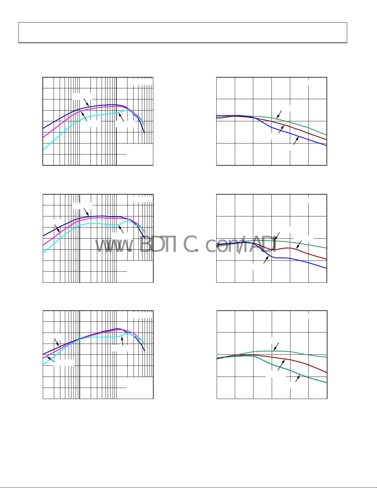
TYPICAL PERFORMANCE CHARACTERISTICS
VIN = 3.6 V, L = 2.2 µH, CIN = 2.2 µF, C
100
95
90
85
VIN = 2.7V
= 4.7 µF, unless otherwise noted.
OUT
TA = 25°C
1.22
TA = 25°C
1.21
VIN = 2.7V
80
75
EFFICIENCY (%)
70
65
60
1 10 100 1000
Figure 4. Efficiency vs. Load Current (V
100
95
90
VIN = 3.6V
85
80
75
EFFICIENCY (%)
70
65
60
1 10 100 1000
Figure 5. Efficiency vs. Load Current (V
VIN = 3.6V
LOAD CURRENT (mA)
VIN = 2.7V
LOAD CURRENT (mA)
VIN = 4.5V
OUT
VIN = 4.5V
OUT
MODE = PSM
L = 2.2µH
C
= 2.2µF
IN
C
= 10µF
OUT
= 1.2 V)
TA = 25°C
MODE = PSM
L = 2.2µH
C
= 2.2µF
IN
C
= 10µF
OUT
= 1.5 V)
1.20
OUTPUT VOLTAGE (V)
1.19
1.18
06631-004
0 100 200 300 400 500 600
Figure 7. Output Voltage Accuracy (V
1.52
1.51
1.50
OUTPUT VOLTAGE (V)
1.49
1.48
06631-005
0 100 200 300 400 500 600
Figure 8. Output Voltage Accuracy (V
VIN = 3.6V
LOAD CURRENT (mA)
VIN = 2.7V
VIN = 4.5V
LOAD CURRENT (mA)
VIN = 4.5V
OUT
VIN = 3.6V
OUT
= 1.2 V)
TA = 25°C
= 1.5 V)
06631-007
06631-020
100
95
90
VIN = 2.7V
85
80
VIN = 3.6V
75
EFFICIENCY (%)
70
65
60
1 10 100 1000
LOAD CURRENT (mA)
VIN = 4.5V
Figure 6. Efficiency vs. Load Current (V
TA = 25°C
MODE = PSM
L = 2.2µH
C
= 2.2µF
IN
C
OUT
= 1.8 V)
OUT
= 10µF
06631-006
Rev. B | Page 6 of 24
1.82
1.81
VIN = 2.7V
1.80
OUTPUT VOLTAGE (V)
1.79
1.78
0 100 200 300 400 500 600
VIN = 3.6V
VIN = 4.5V
LOAD CURRENT (mA)
Figure 9. Output Voltage Accuracy (V
= 1.8 V)
OUT
TA = 25°C
06631-009
ADP2102
www.BDTIC.com/ADI
100
EFFICIENCY (%)
TA = 25°C
C
= 6.8pF
FF
95
90
85
VIN = 4.5V
VIN = 5.0V
VIN = 5.5V
1.53
1.52
PSM
1.51
1.50
CCM
OUTPUT VOLTAGE (V)
1.49
TA = 25°C
80
1 10 100 1000
LOAD CURRENT (mA)
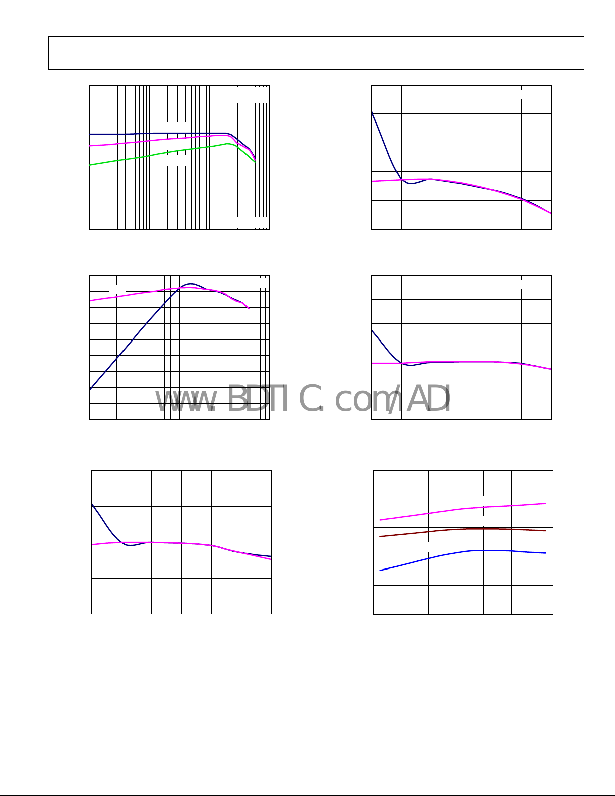
Figure 10. Efficiency vs. Load Current (V
95
90
85
80
75
70
EFFICIENCY (%)
65
60
55
50
PSM
CCM
10 100 1k
LOAD CURRENT (mA)
Figure 11. PSM vs. CCM Efficiency (V
1.22
1.21
PSM
1.20
CCM
OUTPUT VOLTAGE (V)
1.19
MODE = PSM
= 3.3 V)
OUT
= 1.8 V)
OUT
TA = 25°C
TA = 25°C
1.48
06631-050
0 100 200 300 400 500 600
Figure 13. Output Voltage vs. Load Current (V
1.84
1.83
1.82
PSM
1.81
CCM
1.80
OUTPUT VOLTAGE (V)
1.79
1.78
06631-026
0 100 200 300 400 500 600
Figure 14. Output Voltage vs. Load Current (V
1.23
1.22
1.21
1.20
OUTPUT VOL TAGE (V)
1.19
LOAD CURRENT (mA)
LOAD CURRENT (mA)
I
= 300mA
LOAD
I
= 600mA
LOAD
I
LOAD
= 0mA
= 1.5 V)
OUT
TA = 25°C
= 1.8 V)
OUT
06631-013
06631-017
1.18
0 100 200 300 400 500 600
Figure 12. Output Voltage vs. Load Current (V
LOAD CURRENT (mA)
= 1.2 V)
OUT
06631-011
Rev. B | Page 7 of 24
1.18
–45 –25 –5 15 35 55 75
Figure 15. Output Voltag
TEMPERATURE ( °C)
e vs. Temperature (V
OUT
= 1.2 V)
06631-046
ADP2102
www.BDTIC.com/ADI
1.52
1.51
1.50
I
= 0mA
LOAD
I
= 300mA
1.49
1.48
OUTPUT VOLTAGE (V)
1.47
1.46
–40 –15 10 35 60 85
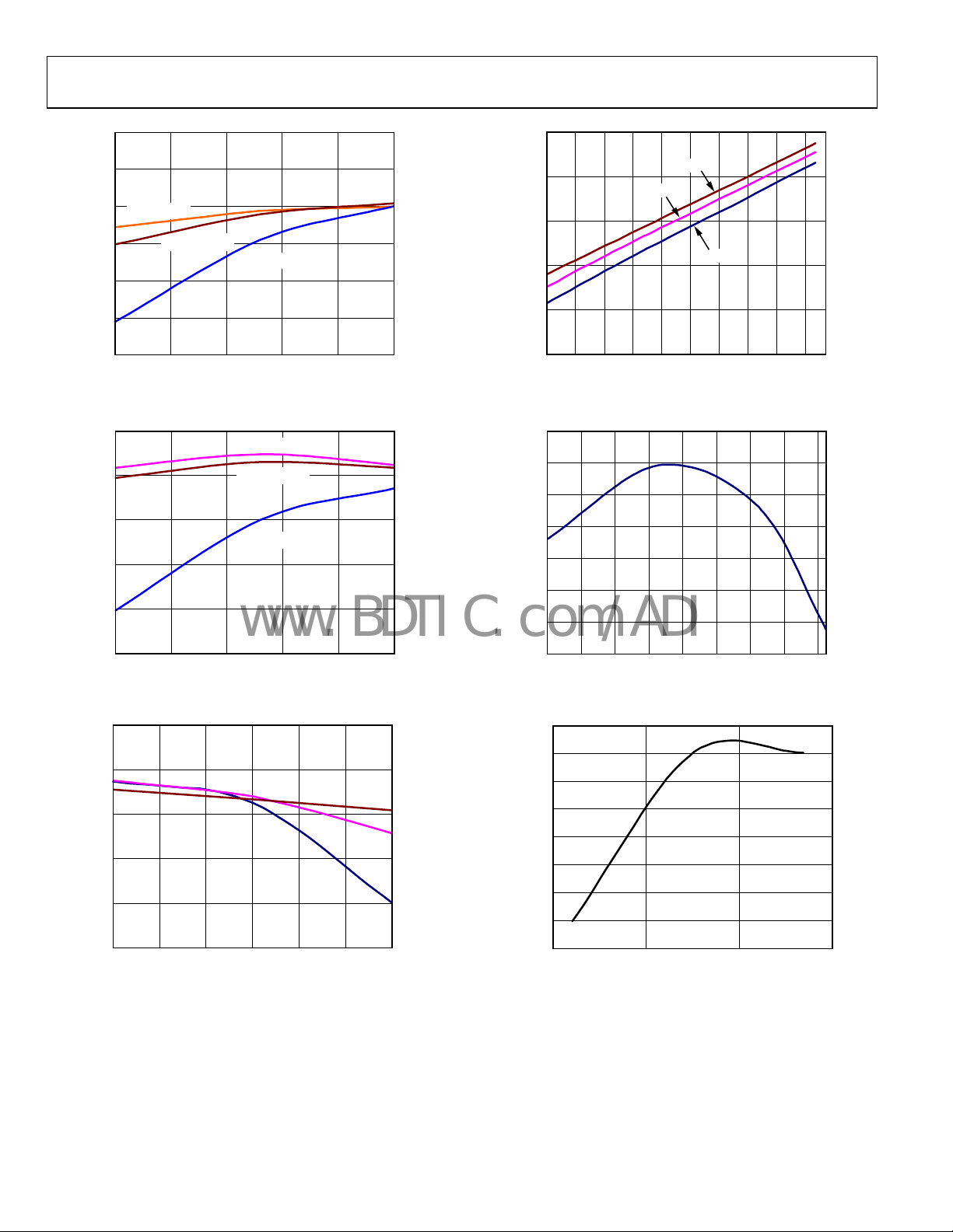
Figure 16. Output Voltag
1.81
1.80
1.79
1.78
OUTPUT VOLTAGE (V)
1.77
LOAD
I
= 600mA
LOAD
TEMPERATURE ( °C)
e vs. Temperature (V
I
= 0mA
LOAD
I
= 300mA
LOAD
I
= 600mA
LOAD
= 1.5 V)
OUT
06631-047
85
80
75
70
QUIESCENT CURRENT (µA)
65
60
2.7 3.0 3.3 3.6 3.9 4.2 4.5 4.8 5.1 5.4
INPUT VOLTAGE (V)
+85°C
+25°C
–40°C
Figure 19. Quiescent Current vs. Input Voltage
77
76
75
74
73
72
QUIESCENT CURRENT (µA)
71
06631-045
1.76
–40 –15 10 35 60 85
Figure 17. Output Voltag
3.40
3.36
3.32
3.28
OUTPUT VOLTAGE (V)
3.24
3.20
0 100 200 300 400 500 600
Figure 18. Output Voltage Accuracy (V
TEMPERATURE (° C)
e vs. Temperature (V
LOAD CURRENT (mA)
+85°C
+25°C
–40°C
= 3.3 V)
OUT
OUT
= 1.8 V)
70
06631-048
–40 –20 0 20 40 60 80 100 120
TEMPERATURE (° C)
06631-053
Figure 20. Quiescent Current vs. Temperature
0.8005
0.8000
0.7995
0.7990
0.7985
0.7980
FEEDBACK VOLT AGE (V)
0.7975
0.7970
0.7965
06631-049
–50 0 50 100
TEMPERATURE ( °C)
V
= 3.6V
IN
06631-021
Figure 21. Feedback Voltage vs. Temperature
Rev. B | Page 8 of 24
 Loading...