ANALOG DEVICES ADP198 Service Manual

Logic Controlled, 1 A, High-Side Load
Switch with Reverse Current Blocking
Data Sheet
FEATURES
Low RDSON of 50 mΩ @ 3.3 V (WLCSP only)
Low input voltage range: 1.65 V to 6.5 V
1 A continuous operating current
Built-in level shift for control logic that can be operated by
1.2 V logic
Low 2.5 μA quiescent current @ V
Low 1.1 μA shutdown current @ V
Reverse current blocking
Programmable start-up time
Ultrasmall 1 mm × 1 mm, 4-ball, 0.5 mm pitch (WLCSP)
Tiny 8-lead lead frame chip scale package (LFCSP)
2.0 mm × 2.0 mm × 0.55 mm, 0.5 mm pitch
APPLICATIONS
Mobile phones
Digital cameras and audio devices
Portable and battery-powered equipment
= 2.8 V
IN
= 2.8 V
IN
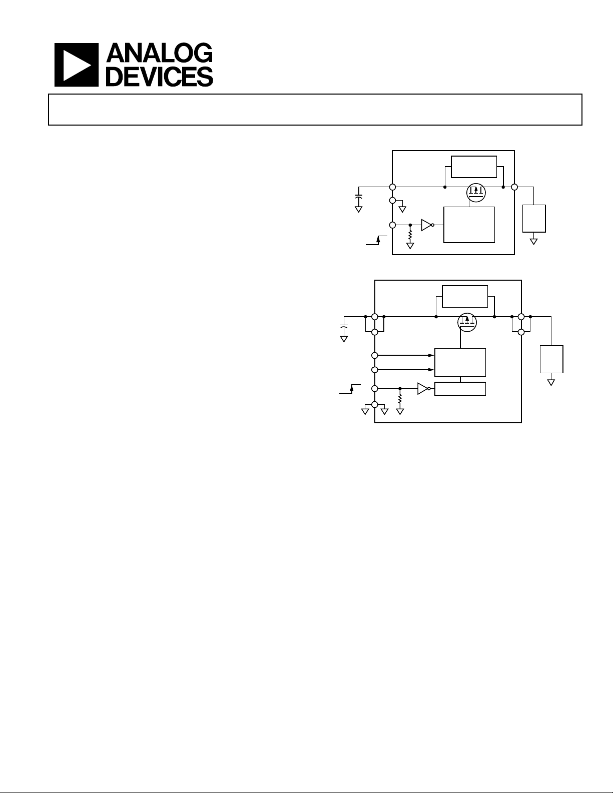
TYPICAL APPLICATION CIRCUITS
ADP198
VIN
+
GND
EN
ON
OFF
Figure 1. WLCSP
ADP198
VIN
+
VIN VOUT
SEL0
SEL1
ON
EN
OFF
GND
REVERSE
POLARITY
PROTECTION
LEVEL SHIFT
AND SLEW
RATE CONTROL
REVERSE
POLARITY
PROTECTION
SLEW
RATE CONTROL
LEVEL SHIFT
ADP198
VOUT
LOAD
09484-001
VOUT
LOAD
GENERAL DESCRIPTION
The ADP198 is a high-side load switch designed for operation
between 1.65 V and 6.5 V that is protected against reverse
current flow from output to input. A load switch provides power
domain isolation, thereby helping to keep subsystems isolated and
powered independently and enabling reduced power consumption.
The ADP198 contains a low on-resistance P-channel MOSFET
that supports more than 1 A of continuous load current. The
low 2.5 μA quiescent current and ultralow shutdown current
make the ADP198 ideal for battery-operated portable
Figure 2. LFCSP
equipment. The built-in level shifter for enable logic makes the
ADP198 compatible with modern processors and general-purpose
input/output (GPIO) controllers. The LFCSP version also allows
the user to program the start-up time to control the inrush
current at turn on.
The ADP198 is available in an ultrasmall 1 mm × 1 mm, 4-ball,
0.5 mm pitch WLCSP. An 8-lead, 2 mm × 2 mm × 0.55 mm,
0.5 mm pitch LFCSP is also available.
09484-002
Rev. D
Information furnished by Analog Devices is believed to be accurate and reliable. However, no
responsibility is assumed by Analog Devices for its use, nor for any infringements of patents or other
rights of third parties that may result from its use. Specifications subject to change without notice. No
license is granted by implication or otherwise under any patent or patent rights of Analog Devices.
Trademarks and registered trademarks are the property of their respective owners.
One Technology Way, P.O. Box 9106, Norwood, MA 02062-9106, U.S.A.
Tel: 781.329.4700 www.analog.com
Fax: 781.461.3113 ©2011–2012 Analog Devices, Inc. All rights reserved.

ADP198 Data Sheet
TABLE OF CONTENTS
Features .............................................................................................. 1
Applications ....................................................................................... 1
Typical Application Circuits ............................................................ 1
General Description ......................................................................... 1
Revision History ............................................................................... 2
Specifications ..................................................................................... 3
Absolute Maximum Ratings ....................................................... 5
Thermal Data ................................................................................ 5
Thermal Resistance ...................................................................... 5
ESD Caution .................................................................................. 5
Pin Configurations and Function Descriptions ........................... 6
REVISION HISTORY
6/12—Rev. C to Rev. D
Changes to Table Headings in Table 6 ......................................... 14
Added Text to Diode OR’ing Applications Section .................... 15
Updated Outline Dimensions ....................................................... 16
4/12—Rev. B to Rev. C
Changes to VOUT Time Parameters ............................................. 3
11/11—Rev. A to Rev. B
Changes to WLCSP Turn-On Delay Time Parameter ................. 3
Changes to Ordering Guide .......................................................... 16
10/11—Rev. 0 to Rev. A
Change to Features Section ............................................................. 1
Changes to Table 1, Specifications Section ................................... 3
Change to Ground Current Section ............................................. 12
Changes to Enable Feature Section .............................................. 13
Updated Outline Dimensions ....................................................... 16
10/11—Revision 0: Initial Version
Typical Performance Characteristics ..............................................8
Theory of Operation ...................................................................... 11
Applications Information .............................................................. 12
Ground Current .......................................................................... 12
Enable Feature ............................................................................ 13
Timing.......................................................................................... 14
Diode OR’ing Applications ....................................................... 15
Packaging and Ordering Information ......................................... 16
Outline Dimensions ................................................................... 16
Ordering Guide .......................................................................... 16
Rev. D | Page 2 of 16

Data Sheet ADP198
High
VIH
VIN ≤ 5 V, TJ = −40°C to +85°C
1.2
V
VIN = 1.65 V, I
= 200 mA, VEN = 1.5 V
180 mΩ
VIN = 1.65 V, I
= 200 mA, VEN = 1.5 V
200 mΩ
VIN = 3.6 V, I
= 200 mA, VEN = 1.5 V, C
= 1 μF; SEL0 = H, SEL1 = H
1100
μs
SPECIFICATIONS
VIN = 2.8 V, EN = VIN, I
Table 1.
Parameter Symbol Test Conditions/Comments Min Typ Max Unit
INPUT VOLTAGE RANGE VIN TJ = −40°C to +85°C 1.65 6.5 V
EN INPUT
Threshold
5 V < VIN, TJ = −40°C to +85°C 1.3 V
Low VIL 1.65 V ≤ VIN ≤ 6.5 V, TJ = −40°C to +85°C 0.43 V
Pull-Down Current IEN 500 nA
REVERSE BLOCKING
V
Current VEN = 0, VIN = 0, V
OUT
VEN = 0, VIN = 0, V
Hysteresis |VIN − V
CURRENT
Quiescent Current IQ I
VIN = V
VIN = V
Off State Current I
EN = GND, TJ = −40°C to +85°C 2 µA
EN = GND, V
VIN to VOUT RESISTANCE RDSON
WLCSP VIN = 5 V, I
VIN = 3.3 V, I
VIN = 2.8 V, I
VIN = 1.8 V, I
LFCSP VIN = 5 V, I
VIN = 3.3 V, I
VIN = 2.8 V, I
VIN = 1.8 V, I
VOUT TIME
WLCSP
Turn-On Delay Time t
ADP198ACBZ-11-R7 VIN = 3.6 V, I
LFCSP
Turn-On Delay Time t
VIN = 3.6 V, I
VIN = 3.6 V, I
= 200 mA, TA = 25°C, unless otherwise noted.
OUT
= 6.5 V 7 µA
OUT
= 6.5 V, TJ = −40°C to +85°C 13 µA
OUT
| 75 mV
OUT
= 0 mA, TJ = −40°C to +85°C, includes EN pull-down current
OUT
= 2.8 V 2.5 µA
OUT
= 6.5 V 20 µA
OUT
EN = GND 1.1 µA
OFF
= 0 V, TJ = −40°C to +85°C 2 µA
OUT
= 200 mA, VEN = 1.5 V 40 mΩ
LOAD
= 200 mA, VEN = 1.5 V 50 80 mΩ
LOAD
= 200 mA, VEN = 1.5 V 60 mΩ
LOAD
= 200 mA, VEN = 1.5 V 130 mΩ
LOAD
LOAD
= 200 mA, VEN = 1.5 V 75 120 mΩ
LOAD
= 200 mA, VEN = 1.5 V 90 mΩ
LOAD
= 200 mA, VEN = 1.5 V 100 mΩ
LOAD
= 200 mA, VEN = 1.5 V 120 mΩ
LOAD
LOAD
VIN = 3.6 V, I
ON _D LY
VIN = 3.6 V, I
ON_DLY
= 200 mA, VEN = 1.5 V, C
LOAD
= 200 mA, VEN = 1.5 V, C
LOAD
= 200 mA, VEN = 1.5 V, C
LOAD
= 200 mA, VEN = 1.5 V, C
LOAD
= 200 mA, VEN = 1.5 V, C
LOAD
LOAD
= 1 μF 7 μs
LOAD
= 1 μF 450 μs
LOAD
= 1 μF; SEL0 = L, SEL1 = L 30 μs
LOAD
= 1 μF; SEL0 = H, SEL1 = L 200 μs
LOAD
= 1 μF; SEL0 = L, SEL1 = H 450 μs
LOAD
LOAD
Rev. D | Page 3 of 16

ADP198 Data Sheet
V
EN
V
OUT
TURN-ON
RISE
90%
10%
TURN-OFF
DELAY
TURN-OFF
FALL
TURN-ON
DELAY
09484-003
Timing Diagram
Figure 3. Timing Diagram
Rev. D | Page 4 of 16

Data Sheet ADP198
VIN to GND Pins
−0.3 V to +7 V
Stresses a bove those listed under Absolute Maximum Ratings
may cause permanent damage to the device. This is a stress
rating only; functional operation of the device at these or any
other conditions above those indicated in the operational
section of this specification is not implied. Exposure to absolute
maximum rating conditions for extended periods may affect
device reliability.
ABSOLUTE MAXIMUM RATINGS
Table 2.
Parameter Rating
VOUT to GND Pins −0.3 V to +7 V
EN to GND Pins −0.3 V to +7 V
Continuous Drain Current
TA = 25°C ±1000 mA
TA = 85°C ±1000 mA
Storage Temperature Range −65°C to +150°C
Operating Junction Temperature Range −40°C to +125°C
Soldering Conditions JEDEC J-STD-020
THERMAL DATA
Absolute maximum ratings apply individually only, not in
combination. The ADP198 can be damaged if the junction
temperature limits are exceeded. Monitoring ambient temperature
does not guarantee that T
limits. In applications with high power dissipation and poor
thermal resistance, the maximum ambient temperature may
need to be derated.
In applications with moderate power dissipation and low
printed circuit board (PCB) thermal resistance, the maximum
ambient temperature can exceed the maximum limit as long
as the junction temperature is within specification limits. The
junction temperature (T
ambient temperature (T
(P
), and the junction-to-ambient thermal resistance of the
D
package (θ
).
JA
Maximum junction temperature (T
ambient temperature (T
formula
T
= TA + (PD × θJA)
J
is within the specified temperature
J
) of the device is dependent on the
J
), the power dissipation of the device
A
) is calculated from the
J
) and power dissipation (PD) using the
A
The junction-to-ambient thermal resistance (θ
is based on modeling and calculation using a 4-layer board. The
junction-to-ambient thermal resistance is highly dependent on
the application and board layout. In applications where high
maximum power dissipation exists, close attention to thermal
board design is required. The value of θ
may vary, depending on
JA
PCB material, layout, and environmental conditions. The specified values of θ
are based on a 4-layer, 4 inch × 3 inch PCB. Refer
JA
to JESD 51-7 and JESD 51-9 for detailed information regarding
board construction. For additional information, see the AN-617
Application Note, MicroCSP™ Wafer Level Chip Scale Package.
Ψ
is the junction-to-board thermal characterization parameter
JB
with units of °C/W. The Ψ
of the package is based on modeling
JB
and calculation using a 4-layer board. The JESD51-12, Guidelines
for Reporting and Using Package Thermal Information, states that
thermal characterization parameters are not the same as thermal
resistances. Ψ
measures the component power flowing through
JB
multiple thermal paths rather than a single path as in thermal
resistance, θ
from the top of the package as well as radiation from the package,
factors that make Ψ
Maximum junction temperature (T
board temperature (T
. Therefore, ΨJB thermal paths include convection
JB
more useful in real-world applications.
JB
) is calculated from the
J
) and power dissipation (PD) using the
B
formula
T
= TB + (PD × ΨJB)
J
Refer to JESD51-8, JESD51-9, and JESD51-12 for more detailed
information about Ψ
.
JB
THERMAL RESISTANCE
θJA and ΨJB are specified for the worst-case conditions, that is, a
device soldered in a circuit board for surface-mount packages.
Table 3. Thermal Resistance
Package Type θJA θJC ΨJB Unit
4-Ball, 0.5 mm Pitch WLCSP 260 4 58.4 °C/W
8-Lead, 2 mm × 2 mm LFCSP 72.1 42.3 47.1 °C/W
ESD CAUTION
) of the package
JA
Rev. D | Page 5 of 16
 Loading...