ADP1878/ADP1879
COMP
BST
FB
DRVH
GND
SW
VREG
RES
DRVL
SS
C
SS
PGND
VIN
C
C
C
VREG
C
VREG2
C
C2
R
C
R
BOT
R
TOP
V
OUT
EN
10kΩ
V
REG
Q1
Q2
L
C
OUT
V
OUT
C
BST
LOAD
C
IN
VIN = 2.95V TO 20V
ADP1878/
ADP1879
R
RES
PGOOD
R
PGD
V
EXT
09441-001
100
95
90
85
80
75
70
65
60
55
50
45
40
35
30
25
10 100 1k 10k 100k
EFFICIENCY (%)
LOAD CURRENT ( mA)
TA = 25°C
V
OUT
= 1.8V
f
SW
= 300kHz
WÜRTH INDUCT OR:
744325120, L = 1.2µH, DCR = 1.8mΩ
INFINEON FETs:
BSC042N03MS G (UPP E R/LOWER)
V
IN
= 5V (PSM)
VIN = 13V (PSM)
VIN = 16.5V (PSM)
VIN = 13V
VIN = 16.5V
09441-102
Constant On Time and Valley Current Mode
Data Sheet
FEATURES
Power input voltage range: 2.95 V to 20 V
On-board bias regulator
Minimum output voltage: 0.6 V
0.6 V reference voltage with ±1.0% accuracy
Supports all N-channel MOSFET power stages
Available in 300 kHz, 600 kHz, and 1.0 MHz options
No current sense resistor required
Power saving mode (PSM) for light loads (ADP1879 only)
Resistor programmable current limit
Power good with internal pull-up resistor
Externally programmable soft start
Thermal overload protection
Short-circuit protection
Standalone precision enable input
Integrated bootstrap diode for high-side drive
Starts into a precharged output
Available in a 14-lead LFCSP_WD package
Synchronous Buck Controller with
TYPICAL APPLICATIONS CIRCUIT
Figure 1.
APPLICATIONS
Telecommunications and networking systems
Mid-to-high end servers
Set-top boxes
DSP core power supplies
GENERAL DESCRIPTION
The ADP1878/ADP1879 are versatile current-mode, synchronous
step-down controllers. They provide superior transient response,
optimal stability, and current-limit protection by using a constant
on time, pseudo fixed frequency with a programmable current-limit,
current control scheme. These devices offer optimum performance
at low duty cycles by using a valley, current-mode control architecture allowing the ADP1878/ADP1879 to drive all N-channel power
stages to regulate output voltages to as low as 0.6 V.
The ADP1879 is the power saving mode (PSM) version of the
device and is capable of pulse skipping to maintain output
regulation while achieving improved system efficiency at light
loads (see the ADP1879 Power Saving Mode (PSM) section for
more information).
Available in three frequency options (300 kHz, 600 kHz, and
1.0 MHz) plus the PSM option, the ADP1878/ADP1879 are well
suited for a wide range of applications that require a single input
power supply range from 2.95 V to 20 V. Low voltage biasing is
supplied via a 5 V internal low dropout regulator (LDO). In
addition, soft start programmability is included to limit input
inrush current from the input supply during startup and to
provide reverse current protection during precharged output
Rev. 0
Information furnished by Analog Devices is believed to be accurate and reliable. However, no
responsibility is assumed by Analog Devices for its use, nor for any infringements of patents or other
rights of third parties that may result from its use. Specifications subject to change without notice. No
license is granted by implication or otherwise under any patent or patent rights of Analog Devices.
Trademarks and registered trademarks are the property of their respective owners.
conditions. The low-side current sense, current gain scheme and
integration of a boost diode, together with the PSM/forced
pulse-width modulation (PWM) option, reduce the external
device count and improve efficiency.
The ADP1878/ADP1879 operate over the −40°C to +125°C
junction temperature range and are available in a 14-lead
LFCSP_WD package.
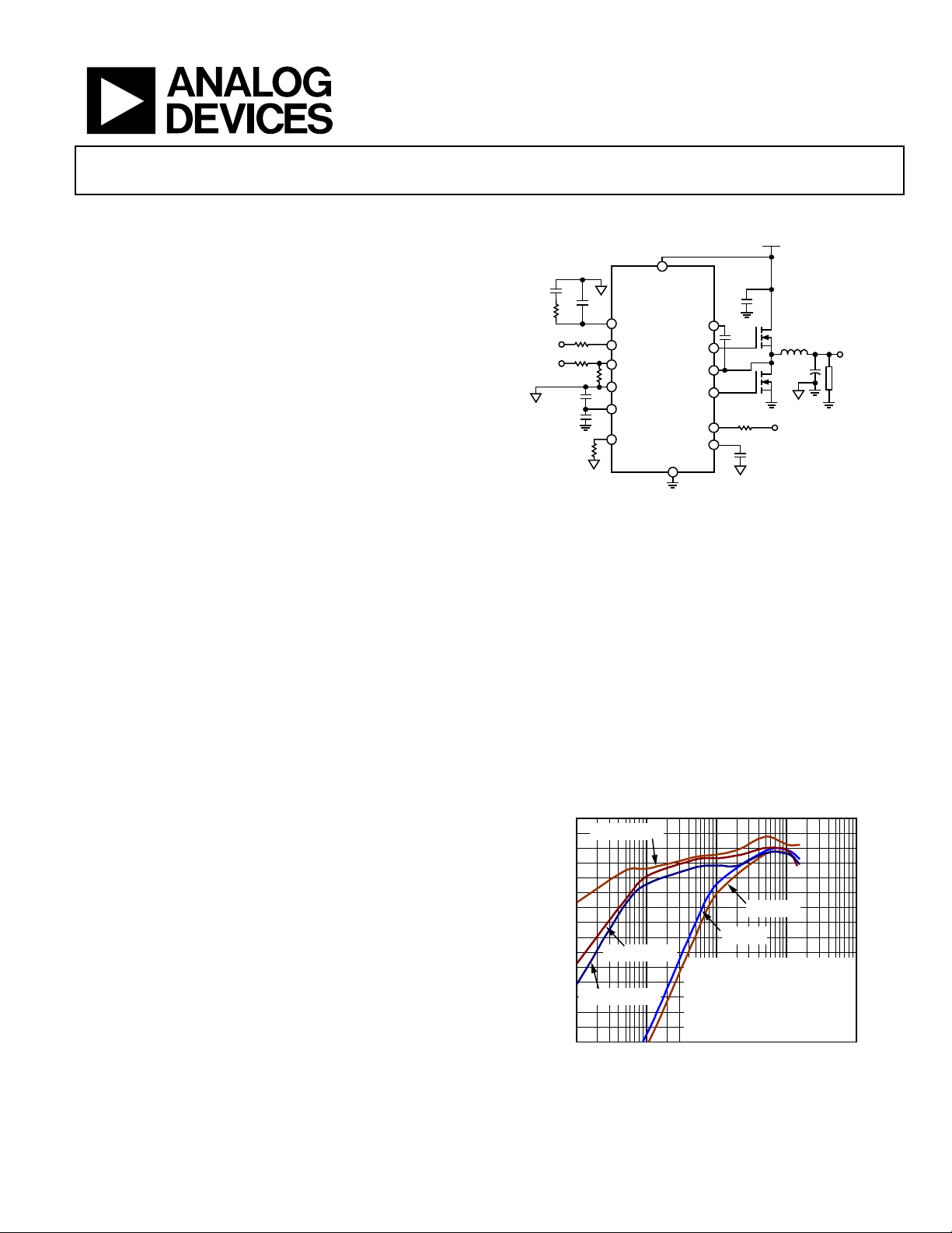
Figure 2. ADP1878/ADP1879 Efficiency vs. Load Current (V
One Technology Way, P.O. Box 9106, Norwood, MA 02062-9106, U.S.A.
Tel: 781.329.4700
Fax: 781.461.3113 ©2011 Analog Devices, Inc. All rights reserved.
= 1.8 V, 300 kHz)
OUT
www.analog.com
 Loading...