Dual Output Synchronous Buck
V
FEATURES
Input voltage range: 2.75 V to 14.5 V
Output voltage range: 0.6 V to 90% V
Maximum output current greater than 25 A per channel
Programmable frequency: 200 kHz to 1.5 MHz
Flex-Mode architecture with integrated drivers
180° phase shift minimizes input ripple current and required
input capacitance
±0.85% output voltage accuracy −40°C to +85°C
Integrated boost diodes
Pulse skip high efficiency mode under light load
Power good with internal pull-up resistor
Overvoltage and overcurrent limit protection
Thermal overload protection
Input undervoltage lockout (UVLO)
Externally adjustable soft start, slope compensation and
current sense gain
Independent precision enable inputs
Synchronization input
Suitable for any output capacitors
Available in 32-lead 5 mm × 5 mm LFCSP
APPLICATIONS
Set top boxes
Printers
Communication infrastructure
Distributor power dc systems
Industrial and instrumentation
GENERAL DESCRIPTION
The ADP1877 is a Flex-Mode™ (proprietary architecture of
Analog Devices, Inc.), dual-channel, step-down switching
controller with integrated drivers that drive N-channel
synchronous power MOSFETs. The two PWM outputs are
phase shifted 180°, which reduces the input RMS current, thus
minimizing required input capacitance.
The boost diodes are built into the ADP1877, thus lowering the
overall system cost and component count. The ADP1877 can
be set to operate in pulse skip high efficiency mode under light
load or in PWM continuous conduction mode.
The ADP1877 includes externally adjustable soft start, output
overvoltage protection, externally adjustable current limit,
power good, and a programmable oscillator frequency that
IN
PWM Controller
ADP1877
ranges from 200 kHz to 1.5 MHz. The ADP1877 provides an
output voltage accuracy of ±0.85% from −40°C to +85°C and
±1.5% from −40°C to 125°C in junction temperature. This part
can be powered from a 2.75 V to 14.5 V supply, operates over
o
the −40
ble in a 32-lead 5 mm × 5 mm LFCSP package.
C to +125oC junction temperature range, and is availa-
R
CSG1
R
RAMP2
R
CSG2
= 3.3V PWM
V
O
IN
M1
L1
R
TOP1
M2
M3
M4
VIN = 12V, 300kHz
R
R
VIN
L2
TOP2
R
R
AMP1
RAMP1
EN1
EN2
VDL
VCCO
PGOOD1
PGOOD2
TRK1
TRK2
SYNC
FREQ
COMP1
COMP2
SS1
SS2
AGND
VIN
DH1
BST1
SW1
ILIM1
FB1
DL1
PGND1
RAMP2
DH2
BST2
SW2
ILIM2
FB2
DL2
PGND2
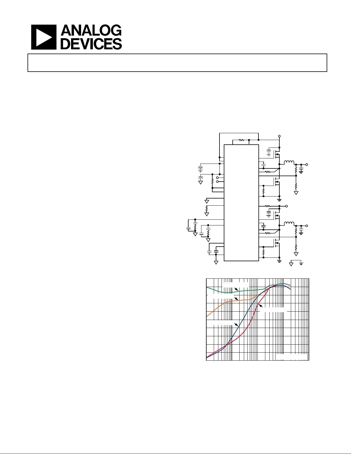
Figure 1. Typical Operation Circuit
100
V
= 1.8V PSM
O
= 1.8V PW M
V
O
VO = 3.3V PSM
LOAD (A)
90
80
70
60
50
40
EFFICIENCY (%)
30
20
10
0
0.01 0.1 1 10 100
Figure 2. Efficiency Plot of Figure 42, 20 A Output
BOT1
BOT2
VOUT1
VOUT2
08299-002
08299-001
Rev. C
Information furnished by Analog Devices is believed to be accurate and reliable. However, no
responsibility is assumed by Analog Devices for its use, nor for any infringements of patents or
other rights of third parties that may result from its use. Specifications subject to change without
notice. No license is granted by implication or otherwise under any patent or patent rights of
Analog Devices. Trademarks and registered trademarks are the property of their respective
owners.
One Technology Way, P.O. Box 9106, Norwood, MA 02062-9106, U.S.A.
Tel: 781.329.4700 www.analog.com
Fax: 781.461.3113 ©2009–2010 Analog Devices, Inc. All rights reserved.

ADP1877
TABLE OF CONTENTS
Features .............................................................................................. 1
Applications ....................................................................................... 1
General Description ......................................................................... 1
Revision History ............................................................................... 2
Specifications ..................................................................................... 3
Absolute Maximum Ratings ............................................................ 6
ESD Caution .................................................................................. 6
Simplified Block Diagram ............................................................... 7
Pin Configuration and Function Descriptions ............................. 8
Typical Performance Characteristics ........................................... 10
Theory of Operation ...................................................................... 13
Control Architecture .................................................................. 13
Oscillator Frequency .................................................................. 13
Mode of Operation ..................................................................... 14
Synchronization .......................................................................... 14
Soft Start ...................................................................................... 14
Synchronous Rectifier and Dead Time ................................... 15
Input Undervoltage Lockout ..................................................... 15
Internal Linear Regulator .......................................................... 15
Overvoltage Protection .............................................................. 15
Power Good ................................................................................. 15
Short Circuit and Current Limit Protection ........................... 16
Shutdown Control ...................................................................... 16
Thermal Overload Protection ................................................... 16
Applications Information .............................................................. 17
Setting the Output Voltage ........................................................ 17
Soft Start ...................................................................................... 17
Setting the Current Limit .......................................................... 17
Accurate Current Limit Sensing ............................................... 17
Setting the Slope Compensation .............................................. 18
Setting the Current Sense Gain ................................................ 18
Input Capacitor Selection .......................................................... 19
Input Filter ................................................................................... 19
Boost Capacitor Selection ......................................................... 20
Inductor Selection ...................................................................... 20
Output Capacitor Selection ....................................................... 20
MOSFET Selection ..................................................................... 21
Loop Compensation .................................................................. 22
Switching Noise and Overshoot Reduction ............................ 23
Voltage Tracking ......................................................................... 23
Coincident Tracking .................................................................. 23
Ratiometric Tracking ................................................................. 24
PCB Layout Guideline ................................................................... 25
MOSFETs, Input Bulk Capacitor, and Bypass Capacitor ...... 25
High Current and Current Sense Paths ................................... 25
Signal Paths ................................................................................. 25
PGND Plane ................................................................................ 25
Feedback and Current Limit Sense Paths ............................... 25
Switch Node ................................................................................ 26
Gate Driver Paths ....................................................................... 26
Output Capacitors ...................................................................... 26
Typical Operating Circuits ............................................................ 27
Outline Dimensions ....................................................................... 31
Ordering Guide .......................................................................... 31
REVISION HISTORY
4/10—Rev. B to Rev. C
Changes to Features and General Description ............................. 1
Changes to Quiescent Current Parameter and FB to TRK Offset
Voltage Parameter, Table 1 .............................................................. 3
Changes to Theory of Operation Section .................................... 13
Changes to Setting the Slope Compensation Section ................ 18
11/09—Rev. A to Rev. B
Changes to Product Title ................................................................. 1
Changes to Signal Path Section .................................................... 25
Rev. C | Page 2 of 32
9/09—Rev. 0 to Rev. A
Changes to Features Section, General Description Section, and
Figure 2 ............................................................................................... 1
Changes to Output Characteristics, Feedback Accuracy Voltage
Parameter; Error Amplifier, Transconductance Parameter; and
Linear Regulator, VCCO Load Regulation and VIN to VCCO
Dropout Voltage Parameters, Table 1 ............................................. 3
Changes to Pin 4, Pin 16, and Pin 25 Descriptions, Table 3 ........ 8
Changes to Figure 5 and Figure 6 ................................................. 10
9/09—Revision 0: Initial Version

ADP1877
SPECIFICATIONS
All limits at temperature extremes are guaranteed via correlation using standard statistical quality control. VIN = 12 V. The specifications
are valid for T
Table 1.
Parameter Symbol Conditions Min Typ Max Unit
POWER SUPPLY
Input Voltage VIN 2.75 14.5 V
Undervoltage Lockout Threshold IN
V
Undervoltage Lockout Hysteresis 0.1 V
Quiescent Current IIN
Shutdown Current I
ERROR AMPLIFIER
FB Input Bias Current IFB −100 +1 +100 nA
Transconductance Gm Sink or source 1 µA, TA = 25 oC 440 550 660 µS
Sink or source 1 µA 385 550 715 µS
TRK1, TRK2 Input Bias Current I
CURRENT SENSE AMPLIFIER GAIN ACS
Default setting, R
OUTPUT CHARACTERICTISTICS
Feedback Accuracy Voltage VFB
Line Regulation of PWM ∆VFB/∆VIN ±0.015 %/V
Load Regulation of PWM ∆VFB/∆V
OSCILLATOR
Frequency f
R
R
FREQ to AGND 235 300 345 kHz
FREQ to VCCO 475 600 690 kHz
SYNC Input Frequency Range f
SYNC Input Pulse Width t
SYNC Pin Capacitance to GND C
LINEAR REGULATOR
VCCO Output Voltage
VCCO Load Regulation I
VCCO Line Regulation VIN = 5.5 V to 14.5 V, I
VCCO Current Limit1 VCCO drops to 4 V from 5 V 350 mA
VCCO Short-Circuit Current1 VCCO < 0.5 V 370 400 mA
VIN to VCCO Dropout Voltage2 V
= −40°C to +125°C, unless otherwise specified. Typical values are at TA = 25°C.
J
V
UVLO
rising 2.45 2.6 2.75 V
IN
falling 2.4 2.5 2.6
IN
EN1 = EN2 = V
= 12 V, VFB = V
IN
in PWM mode
CCO
(no switching)
EN1 = EN2 = GND, VIN = 5.5 V or 14.5 V 100 200 µA
IN_SD
0 V < V
TRK
< 1.5 V −100 +1 +100 nA
TRK1/TRK2
Gain resistor connected to DL,
= 47 kΩ ± 5%
R
CSG
Gain resistor connected to DL,
= 22 kΩ ± 5%
R
CSG
= open 10.5 12 13.5 V/V
CSG
Gain resistor connected to DL,
= 100 kΩ ± 5%
R
CSG
= −40°C to +85°C, VFB = 0.6 V
T
J
= −40°C to +125°C, VFB = 0.6 V
T
J
V
COMP
R
OSC
SYNC
100 ns
SYNCMIN
5 pF
SYNC
I
DROPOUT
range 0.9 V to 2.2 V ±0.3 %
COMP
= 340 kΩ to AGND 170 200 235 kHz
FREQ
= 78.7 kΩ to AGND 744 800 856 kHz
FREQ
= 39.2 kΩ to AGND 1275 1500 1725 kHz
FREQ
= 2 × fsw; f
f
SYNC
frequency is 1 × the f
= 25°C, I
T
A
= −40°C to +125°C
T
J
= 0 mA to 100 mA, 35 mV
VCCO
= 100 mA, VIN ≤ 5 V 0.33 V
VCCO
SYNC
= 100 mA
VCCO
= f
; the minimum sync
OSC
set by the resistor
OSC
= 20 mA 10 mV
VCCO
4.5 5.8 mA
2.4 3 3.6 V/V
5.2 6 6.9 V/V
20.5 24 26.5 V/V
−0.85% +0.6 +0.85% V
−1.5% +0.6 +1.5% V
400 3000 kHz
4.8 5.0 5.18 V
4.7 5.0 5.3 V
Rev. C | Page 3 of 32

ADP1877
Parameter Symbol Conditions Min Typ Max Unit
LOGIC INPUTS
EN1, EN2 EN1/EN2 rising 0.57 0.63 0.68 V
EN1, EN2 Hysteresis 0.03 V
EN1, EN2 Input Leakage Current IEN V
SYNC Logic Input Low 1.3 V
SYNC Logic Input High 1.9 V
SYNC Input Leakage Current I
SYNC = 5 V, internal 1 MΩ pull-down 5 6.5 A
SYNC
GATE DRIVERS
DH Rise Time CDH = 3 nF, V
DH Fall Time CDH = 3 nF, V
DL Rise Time CDL = 3 nF 16 ns
DL Fall Time CDL = 3 nF 14 ns
DH to DL Dead Time External 3 nF is connected to DH and DL 25 ns
DH or DL Driver RON, Sourcing
1
Current
R
Sourcing 2 A with a 100 ns pulse 2 Ω
ON_SOURC
Sourcing 1 A with a 100 ns pulse, VIN = 3 V 2.3 Ω
DH or DL Driver RON, Tempco TC
DH or DL Driver RON, Sinking
Current
1
V
RON
Sinking 2 A with a 100 ns pulse 1.5 Ω
R
ON_SINK
Sinking 1 A with a 100 ns pulse, VIN = 3 V 2 Ω
DH Maximum Duty Cycle f
DH Maximum Duty Cycle f
Minimum DH On Time f
Minimum DH Off Time f
Minimum DL On Time f
COMP VOLTAGE RANGE
COMP Pulse Skip Threshold V
COMP Clamp High Voltage V
In pulse skip mode 0.9 V
COMP,THRES
2.25 V
COMP,HIGH
THERMAL SHUTDOWN
Thermal Shutdown Threshold T
155
TMSD
Thermal Shutdown Hysteresis 20
OVERVOLTAGE AND POWER GOOD
THRESHOLDS
FB Overvoltage Threshold VOV V
FB Overvoltage Hysteresis 40 mV
FB Undervoltage Threshold VUV V
FB Undervoltage Hysteresis 30 mV
TRK INPUT VOLTAGE RANGE 0 5 V
FB TO TRK OFFSET VOLTAGE TRK = 0.5 V to 0.6 V; offset = VFB − V
SOFT START
SS Output Current ISS During start-up 4.6 6.5 8.4 µA
SS Pull-Down Resistor During a fault condition 1 kΩ
= 2.75 V to 14.5 V 1 200 nA
IN
− VSW = 5 V 16 ns
BST
− VSW = 5 V 14 ns
BST
= 3 V or 12 V 0.3 %/oC
IN
= 300 kHz 90 %
OSC
= 1500 kHz 50 %
OSC
= 200 kHz to 1500 kHz 130 ns
OSC
= 200 kHz to 1500 kHz 330 ns
OSC
= 200 kHz to 1500 kHz 280 ns
OSC
°C
°C
rising 0.67 0.7 0.73 V
FB
rising 0.51 0.54 0.57 V
FB
−120 −70 −5 mV
TRK
Rev. C | Page 4 of 32
ADP1877
Parameter Symbol Conditions Min Typ Max Unit
PGOOD
PGOOD Pull-up Resistor R
PGOOD Delay 12 µs
Overvoltage or Undervoltage
Minimum Duration
ILIM1, ILIM2 Threshold Voltage1 Relative to PGND −5 0 +5 mV
ILIM1, ILIM2 Output Current ILIM = PGND 40 50 60
Current Sense Blanking Period
INTEGRATED RECTIFIER
(BOOST DIODE) RESISTANCE
ZERO CURRENT CROSS OFFSET
(SW TO PGND)
1
Guaranteed by design.
2
Connect VIN to VCCO when VIN < 5.5 V. For applications with VIN < 5.5 V and VIN not connected to VCCO, keep in mind that VCCO = VIN − VDROPOUT. VCCO must be ≥
2.75 V for proper operation.
1
Internal pull-up resistor to VCCO 12.5 kΩ
PGOOD
This is the minimum duration required to trip
12 µs
the PGOOD signal.
μA
After DL goes high, current limit is not sensed
100 ns
during this period.
At 20 mA forward current 16 Ω
In pulse skip mode only; f
= 600 kHz 0 2 4 mV
OSC
Rev. C | Page 5 of 32
ADP1877
ABSOLUTE MAXIMUM RATINGS
Table 2.
Parameter Rating
VIN, EN1/EN2, RAMP1/RAMP2 15 V
FB1/FB2, COMP1/COMP2, SS1/SS2,
−0.3 V to +6 V
TRK1/TRK2, FREQ, SYNC, VCCO, VDL,
PGOOD1/PGOOD2
ILIM1/ILIM2 −0.3 V to +16 V
BST1/BST2, DH1/DH2, SW1/SW2 to
−0.3 V to +22 V
PGND1/PGND2
DL1/DL2 to PGND1/PGND2
−0.3 V to VCCO +
0.3 V
BST1/BST2 to PGND1/PGND2, SW1/SW2 to
+25 V
PGND1/PGND2 20 ns Transients
DL1/DL2, SW1/SW2, ILIM1/ILIM2 to
−8 V
PGND1/PGND2 20 ns Negative Transients
PGND1/PGND2 to AGND −0.3 V to +0.3 V
PGND1/PGND2 to AGND 20 ns Transients −8 V to +4 V
θJA, =on a Multilayer PCB (Natural Convection)
1, 2
32.6°C/W
Operating Ambient Temperature Range3 −40°C to +85°C
Operating Junction Temperature Range3 −40°C to +125°C
Storage Temperature Range −65°C to +150°C
Maximum Soldering Lead Temperature 260°C
1
Measured with exposed pad attached to PCB.
2
Junction-to-ambient thermal resistance (θJA) of the package was calculated
or simulated on a multilayer PCB.
3
The device can be damaged when the junction temperature limits are
exceeded. Monitoring ambient temperature does not guarantee that TJ is
within the specified temperature limits. In applications with moderate
power dissipation and low PCB thermal resistance, the maximum ambient
temperature can exceed the maximum limit as long as the junction temperature
is within specification limits. The junction temperature, TJ, of the device is
dependent on the ambient temperature, TA, the power dissipation of the
device, PD, and the junction to ambient thermal resistance of the package,
θJA. Maximum junction temperature is calculated from the ambient
temperature and power dissipation using the formula TJ = TA + PD × θJA.
Stresses above those listed under Absolute Maximum Ratings
may cause permanent damage to the device. This is a stress
rating only and functional operation of the device at these or
any other conditions above those indicated in the operational
section of this specification is not implied. Exposure to absolute
maximum rating conditions for extended periods may affect
device reliability.
Absolute maximum ratings apply individually only, not in
combination. Unless otherwise specified all other voltages are
referenced to GND.
ESD CAUTION
Rev. C | Page 6 of 32
ADP1877
SIMPLIFIED BLOCK DIAGRAM
VCCO
VIN
THERMAL
SHUTDOWN
LDO
REF
OV
0.6V
UV
EN1
EN2
SYNC
FREQ
COMP1
FB1
TRK1
SS1
RAMP1
0.6V
+
–
+
–
1MΩ
ERROR
AMPLIFIER
–
+
G
m
+
+
V
=
0
.
6
R
E
F
6.5µA
LOGIC
FAULT
1kΩ
EN1
SLOPE COMP AND
RAMP GENERATO R
V
OVER_LIM1
OSCILLATOR
3.2V
OV1
DL
DRIVER
OVER_LIM1
UVLO
LOGIC
0.9V
COMPARATOR
CURRENT
CONTROL
PH1
PH2
–
+
–
+
LIMIT
FB1
0.6V
PWM
EN1_SW
EN2_SW
DUPLICATE FOR
CHANNEL 2
OV
UV
SYNC
EN1_SW
OVER_LIM1
OV1
PULSE SKIP
ZERO CROSS
AV = 3, 6, 12, 24
+
–
+
–
DRIVER LOGIC
CONTROL AND
DCM
DETECT
CS GAIN
+
–
OV1
UV1
VCCO
STATE
MACHINE
+
–
–
CURRENT SENSE
AMPLIFIER
+
AGND
VCCO
LOGIC
10kΩ
PGOOD1
BST1
DH1
SW1
VDL
DL1
PGND1
VCCO
50µA
ILIM1
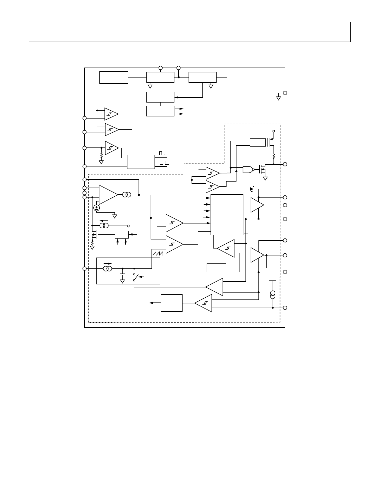
Figure 3. Block Diagram
08299-003
Rev. C | Page 7 of 32

ADP1877
PIN CONFIGURATION AND FUNCTION DESCRIPTIONS
OD1
SS1
TRK1
32
PGO
COMP1
RAMP1
ILIM1
FB1
31
30
BST1
29
28
27
26
25
1EN1
PIN 1
2SYNC
INDICATOR
3VIN
4VCCO
ADP1877
5VDL
TOP VIEW
6
AGND
2
NOTES
1. CONNECT T HE BOTTOM EXPOSED PAD O F THE
LFCSP PACKAGE TO SYSTEM AGND PLANE.
7FREQ
8EN
(Not to S cale)
9
11
10
12
2
FB2
TRK
RAMP2
COMP2
13
SS2
24 SW1
23 DH1
22 PGND1
21 DL1
20 DL2
19 PGND2
18 DH2
17 SW2
14
15
16
ILIM2
BST2
PGOOD2
08299-004
Figure 4. Pin Configuration
Table 3. Pin Function Descriptions
Pin No. Mnemonic Description
1 EN1
Enable Input for Channel 1. Drive EN1 high to turn on the Channel 1 controller, and drive it low to turn off. Tie
EN1 to VIN for automatic startup. For a precision UVLO, put an appropriately sized resistor divider from VIN to
AGND, and tie the midpoint to this pin.
2 SYNC
Frequency Synchronization Input. Accepts an external signal between 1× and 2.3× of the internal oscillator
frequency, f
, set by the FREQ pin. The controller operates in forced PWM when a signal is detected at SYNC or
OSC
when SYNC is high. The resulting switching frequency is ½ of the SYNC frequency. When SYNC is low or left
floating, the controller operates in pulse skip mode.
3 VIN
Connect to Main Power Supply. Bypass with a 1 µF or larger ceramic capacitor connected as close to this pin as
possible and PGND.
4 VCCO
Output of the Internal Low Dropout Regulator (LDO). The internal circuitry and gate drivers are powered from
VCCO. Bypass VCCO to AGND with a 1 F or larger ceramic capacitor. The VCCO output is always active, even
during fault conditions and cannot be turned off even if EN1/EN2 is low. For operations at VIN below 5 V, VIN can
be jumped to VCCO. Do not use the LDO to power other auxiliary system loads.
5 VDL
Power Supply for the Low-Side Driver. Bypass VDL to PGND with a 1 µF or greater ceramic capacitor. Connect
VCCO to VDL.
6 AGND Analog Ground.
7 FREQ
Sets the desired operating frequency between 200 kHz and 1.5 MHz with one resistor between FREQ and AGND.
See Tab le 4 for more details. Connect FREQ to AGND for a preprogrammed 300 kHz or FREQ to VCCO for a 600
kHz operating frequency.
8 EN2
Enable Input for Channel 2. Drive EN2 high to turn on the Channel 2 controller, and drive it low to turn off. Tie
EN2 to VIN for automatic startup. For a precision UVLO, put an appropriately sized resistor divider from VIN to
AGND, and tie the midpoint to this pin.
9 TRK2
Tracking Input for Channel 2. If the tracking function is not used, it is recommended to connect TRK2 to VCCO
through a resistor higher than 1 MΩ, or simply connect TRK2 between 0.7 V and 2 V to reduce the bias current
going into the TRK2 pin.
10 FB2 Output Voltage Feedback for Channel 2. Connect to Channel 2 via a resistor divider.
11 COMP2
Compensation Node for Channel 2. Output of Channel 2 error amplifier. Connect a series resistor-capacitor
network from COMP2 to AGND to compensate the regulation control loop.
12 RAMP2
Programmable Current Setting for Slope Compensation of Channel 2. Connect a resistor from RAMP2 to VIN. The
voltage at RAMP2 is 0.2 V.
13 SS2
Soft Start Input for Channel 2. Connect a capacitor from SS2 to AGND to set the soft start period. This node is
internally pulled up to 3.2 V through a 6.5 µA current source.
Rev. C | Page 8 of 32

ADP1877
Pin No. Mnemonic Description
14 PGOOD2
15 ILIM2
16 BST2
17 SW2
18 DH2
19 PGND2
20 DL2
21 DL1
22 PGND1
23 DH1
24 SW1
25 BST1
26 ILIM1
27 PGOOD1
28 SS1
29 RAMP1
30 COMP1
31 FB1 Output Voltage Feedback for Channel 1. Connect to Channel 1 via a resistor divider.
32 TRK1
33
Bottom
exposed pad
Open-drain power-good indicator logic output with an internal 12 kΩ resistor connected between PGOOD2 and
VCCO. PGOOD2 is pulled to ground when the Channel 2 output is outside the regulation window. An external
pull-up resistor is not required.
Current Limit Sense Comparator Inverting Input for Channel 2. Connect a resistor between ILIM2 and SW2 to set
the current limit offset. For accurate current limit sensing, connect ILIM2 to a current sense resistor at the source
of the low-side MOSFET.
Boot Strapped Upper Rail of High Side Internal Driver for Channel 2. Connect a 0.1 µF to a 0.22 µF multilayer
ceramic capacitor (MLCC) between BST2 and SW2. There is an internal boost rectifier connected between VCCO
and BST2.
Switch Node for Channel 2. Connect to the source of the high-side N-channel MOSFET and the drain of the lowside N-channel MOSFET of Channel 2.
High-Side Switch Gate Driver Output for Channel 2. Capable of driving MOSFETs with total input capacitance up
to 20 nF.
Power Ground for Channel 2. Ground for internal Channel 2 driver. Differential current is sensed between SW2
and PGND2. It is not recommended to short PGND2 to PGND1 directly.
Low-Side Synchronous Rectifier Gate Driver Output for Channel 2. To set the gain of the current sense amplifier,
connect a resistor between DL2 and PGND2. Capable of driving MOSFETs with a total input capacitance up to 20 nF.
Low-Side Synchronous Rectifier Gate Driver Output for Channel 1. To set the gain of the current sense amplifier,
connect a resistor between DL1 and PGND1. Capable of driving MOSFETs with a total input capacitance up to 20 nF.
Power Ground for Channel 1. Ground for internal Channel 1 driver. Differential current is sensed between SW1
and PGND1. It is not recommended to short PGND2 to PGND1 directly.
High-Side Switch Gate Driver Output for Channel 1. Capable of driving MOSFETs with a total input capacitance
up to 20 nF.
Power Switch Node for Channel 1. Connect to the source of the high-side N-channel MOSFET and the drain of
the low-side N-channel MOSFET of Channel 1.
Boot Strapped Upper Rail of High Side Internal Driver for Channel 1. Connect a 0.1 µF to a 0.22 µF multilayer
ceramic capacitor (MLCC) between BST1 and SW1. There is an internal boost diode or rectifier connected
between VCCO and BST1.
Current Limit Sense Comparator Inverting Input for Channel 1. Connect a resistor between ILIM1 and SW1 to set
the current limit offset. For accurate current limit sensing, connect ILIM1 to a current sense resistor at the source
of the low-side MOSFET.
Power Good. Open drain power good indicator logic output with an internal 12 kΩ resistor connected between
PGOOD1 and VCCO. PGOOD1 is pulled to ground when the Channel 1 output is outside the regulation window.
An external pull-up resistor is not required.
Soft Start Input for Channel 1. Connect a capacitor from SS1 to AGND to set the soft start period. This node is
internally pulled up to 3.2 V through a 6.5 µA current source.
Programmable Current Setting for Slope Compensation of Channel 1. Connect a resistor from RAMP1 to VIN. The
voltage at RAMP1 is 0.2 V during operation. This pin is high impedance when the channel is disabled.
Compensation Node for Channel 1. Output of Channel 1 error amplifier. Connect a series resistor-capacitor
network from COMP1 to AGND to compensate the regulation control loop.
Tracking Input for Channel 1. If the tracking function is not used, it is recommended to connect TRK1 to VCCO
through a resistor higher than 1 MΩ, or simply connect TRK1 between 0.7 V and 2 V to reduce the bias current
going into the TRK1 pin.
Connect the bottom exposed pad of the LFCSP package to the system AGND plane.
Rev. C | Page 9 of 32
ADP1877
TYPICAL PERFORMANCE CHARACTERISTICS
100
90
80
70
60
50
40
EFFICIENCY (%)
30
20
10
0
0.01 0.1 1 10
PSM
PWM
LOAD (A)
VIN = 12V
V
OUT
600kHz
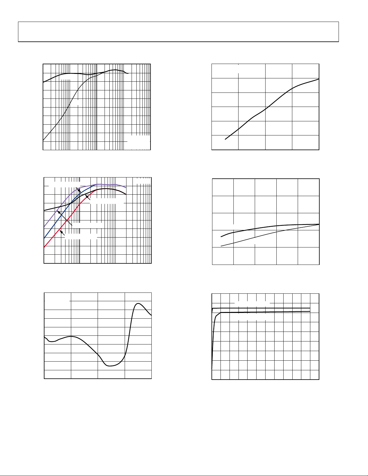
Figure 5. Efficiency Plot of Figure 41, 10 A Output
100
V
= 1.8V PW M
OUT
90
80
V
= 1.05V PSM
70
60
50
40
EFFICIENCY (%)
30
20
10
0
0.01 0.1 1 10
V
OUT
= 1.05V PW M
V
V
= 1.05V_PWM
O
O
OUT
= 1.8V PSM
LOAD (A)
Figure 6. Efficiency Plot of Figure 44, 2 A Output
0.5
VIN = 12V
0.4
V
= 3.3V
OUT
0.3
0.2
0.1
0
–0.1
–0.2
LOAD REGULATION (%)
–0.3
–0.4
–0.5
0 5 10 15 20
LOAD (A)
Figure 7. Load Regulation of Figure 42
= 3.3V
VIN = 3V
100
08299-023
08299-024
08299-025
0.06
V
= 3.3V AT 1A L OAD
OUT
0.05
0.04
0.03
0.02
LINE REGULATION (%)
0.01
0
6 8 10 12 14
VIN (V)
Figure 8. Line Regulation of Figure 42
0
–0.05
–0.10
Δ VCCO (V)
–0.15
–0.20
–0.25
50mA LOAD
100mA LOAD
2.53.03.54.04.55.0
VIN (V)
Figure 9. LDO Load Regulation
5.10
5.05
5.00
4.95
4.90
4.85
VCCO (V)
4.80
4.75
4.70
4.65
5 7 9 11 13 15 17
NO LOAD ON LDO
100mA LOAD ON LDO
VIN (V)
Figure 10. LDO Line Regulation
08299-026
08299-027
08299-028
Rev. C | Page 10 of 32
 Loading...