600 kHz Dual Output Synchronous Buck
ADP1876
RAMP1
R
RAMP1
VIN
DH1
BST1
SW1
ILIM1
FB1
DL1
PGND1
RAMP2
DH2
BST2
SW2
ILIM2
FB2
DL2
PGND2
EN1
EN2
VDL
VCCO
TRK1
1.5V
VINLDO
VOUTLDO
NC
COMP1
COMP2
SS1
SS2
AGND
R
CSG1
R11
R12
R21
R22
M1
M2
R
CSG2
M3
L2
L1
V
OUT1
V
OUT2
V
IN
V
IN
M4
R
RAMP2
PGOOD1
3V to 5V INP UT
PGOOD2
ADP1876
10103-001
PWM Controller with Linear Regulator
Data Sheet
FEATURES
Wide input range: 2.75 V to 20 V
Power stage input voltage: 1 V to 20 V
Output voltage range: 0.6 V up to 90% V
Linear dropout (LDO) regulator with a fixed output
1.5 V at 150 mA
Output current more than 25 A per channel
180º phase shift between channels for reduced input
capacitance
±0.85% reference voltage accuracy from −40°C to +85°C
Integrated boost diodes
Independent channel precision enable
Overcurrent limit protection
Externally programmable soft start, slope compensation,
and current sense gain
Thermal overload protection
Input undervoltage lockout (UVLO)
Power good with internal pull-up resistor
Available in 32-lead, 5 mm × 5 mm LFCSP
IN
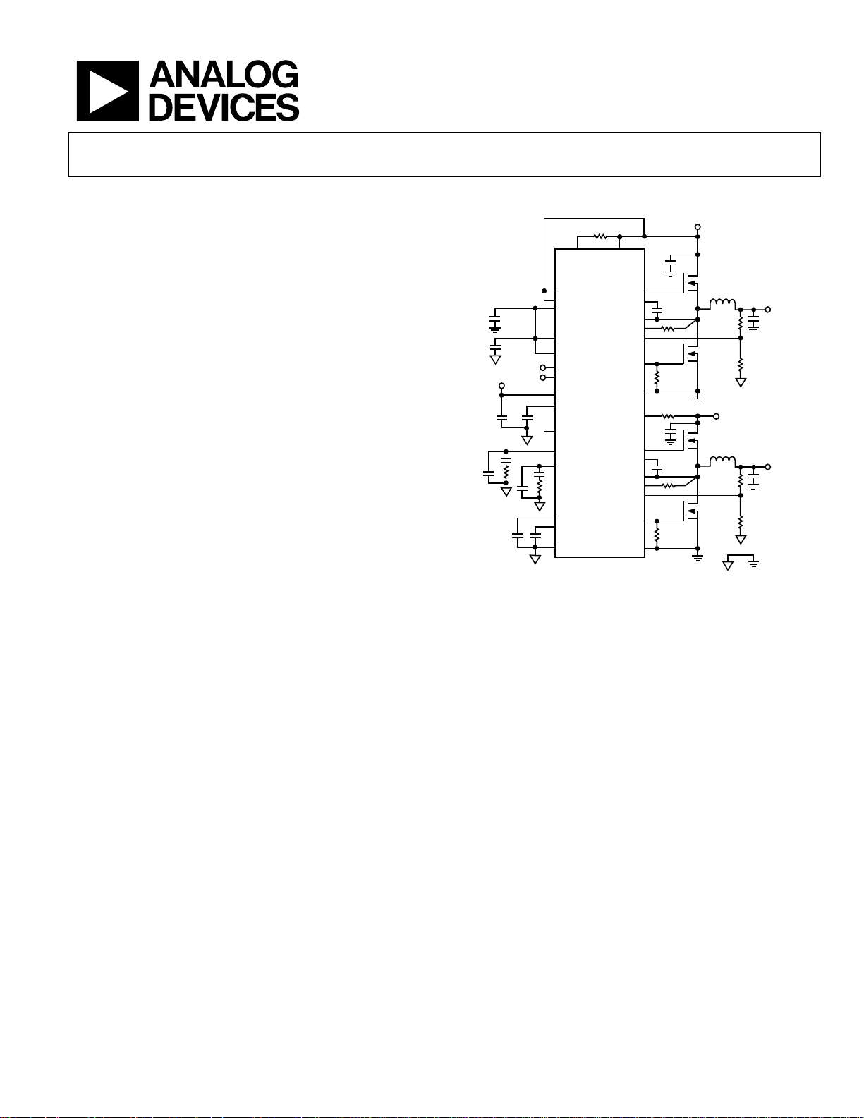
TYPICAL OPERATION CIRCUIT
APPLICATIONS
Consumer applications
Telecommunications base station and networking
Industrial and instrumentation
GENERAL DESCRIPTION
The ADP1876 is a dual output dc-to-dc synchronous buck
controller operating at 600 kHz fixed frequency with integrated
drivers that drive N-channel power MOSFETs. An additional
fixed voltage output, 150 mA linear regulator is available for
powering low power loads. The device operates in current
mode for improved transient response and uses valley current
Rev. A
Information furnished by Analog Devices is believed to be accurate and reliable. However, no
responsibility is assumed by Analog Devices for its use, nor for any infringements of patents or other
rights of third parties that may result from its use. Spe cifications subject to change without n otice. No
license is granted by implication or otherwise under any patent or patent rights of Analog Devices.
Trademarks and registered trademarks are the property of their respective owners.
Figure 1.
sensing for enhanced noise immunity. The two PWM outputs
are phase shifted 180° for reducing the input current ripple and
the required input capacitance.
The ADP1876 provides high speed, high peak current drive
capability with dead time optimization to enable energy
efficient power conversion.
One Technology Way, P.O. Box 9106, Norwood, MA 02062-9106, U.S.A.
Tel: 781.329.4700
Fax: 781.461.3113 ©2011 Analog Devices, Inc. All rights reserved.
www.analog.com

ADP1876 Data Sheet
TABLE OF CONTENTS
Features .............................................................................................. 1
Applications ....................................................................................... 1
Typical Operation Circuit ................................................................ 1
General Description ......................................................................... 1
Revision History ............................................................................... 2
Functional Block Diagram .............................................................. 3
Specifications ..................................................................................... 4
Absolute Maximum Ratings ....................................................... 7
ESD Caution .................................................................................. 7
Pin Configuration and Function Descriptions ............................. 8
Typical Performance Characteristics ........................................... 10
Theory of Operation ...................................................................... 14
Independent Low Dropout Linear Regulator ......................... 14
Controller Architecture ............................................................. 14
Input Undervoltage Lockout ..................................................... 14
Internal Linear Regulator (VCCO) .......................................... 14
Overvoltage Protection .............................................................. 15
Power Good ................................................................................. 15
Short-Circuit and Current-Limit Protection .......................... 15
Shutdown Control ...................................................................... 15
Thermal Overload Protection ................................................... 16
Applications Information .............................................................. 17
Independent Low Dropout Linear Regulator ......................... 17
Setting the Output Voltage of the Controller ......................... 17
Soft Start ...................................................................................... 17
Setting the Current Limit .......................................................... 17
Accurate Current-Limit Sensing .............................................. 17
Setting the Slope Compensation .............................................. 18
Setting the Current Sense Gain ................................................ 18
Input Capacitor Selection .......................................................... 18
Input Filter .................................................................................. 19
Boost Capacitor Selection ......................................................... 19
Inductor Selection ...................................................................... 19
Output Capacitor Selection....................................................... 19
MOSFET Selection ..................................................................... 20
Loop Compensation .................................................................. 21
Switching Noise and Overshoot Reduction ............................ 22
PCB Layout Guideline ............................................................... 23
Typical Applications Circuit ..................................................... 23
Packaging and Ordering Information ......................................... 24
Outline Dimensions ................................................................... 24
Ordering Guide .......................................................................... 24
REVISION HISTORY
11/11—Rev. 0 to Rev. A
Added Evaluation Board to Ordering Guide .............................. 24
9/11—Revision 0: Initial Version
Rev. A | Page 2 of 24
Data Sheet ADP1876
DUPLICATE FOR
CHANNEL 2
BST1
PGND1
+
–
+
–
+
–
+
–
+
–
+
–
FB2
0.6V
OV
UV
PGOOD1
CURRENT SENSE
AMPLIFIER
DH1
DL1
ILIM2
SW1
V
REF
= 0.6V
6.5µA
+
+
–
ERROR
AMPLIFIER
FB1
COMP1
SS1
PWM
COMPARATOR
DL
DRIVER
SLOPE COMP AND
RAMP GENERATOR
CURRENT-
LIMIT
CONTROL
VCCO
RAMP1
50µA
3.2V
g
m
OV1
+
TRK1
CS GAIN
DRIVER LOGIC
CONTROL AND
STATE
MACHINE
OVER_LIM1
PULSE SKIP
OVER_LIM1
LDO
LOGIC
EN1
EN2
VIN
UVLO
OSCILLATOR
600kHz
LINEAR
REGULATOR
VOUTLDO
VINLDO
PH1
PH2
REF
VCCO
OV
UV
0.6V
THERMAL
SHUTDOWN
AGND
0.6V
+
–
+
–
VCCO
ADP1876
VDL
FAULT
OV1
LOGIC
OVER_LIM1
OV1
EN1
EN1_SW
LOGIC
UV1
1kΩ
0.9V
DCM
ZERO CRO S S
DETECT
12kΩ
AV = 3, 6, 12, 24
VCCO
EN1_SW
EN2_SW
NC
–
+
10103-002
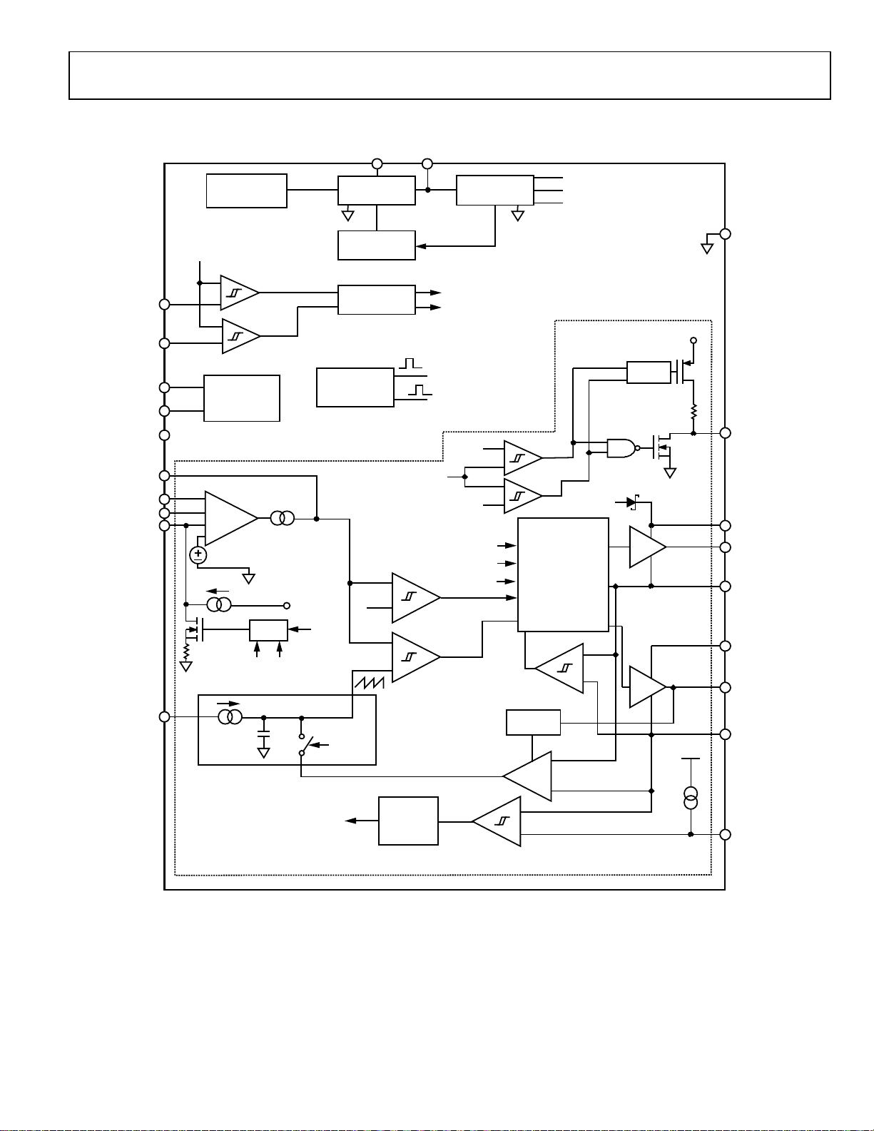
FUNCTIONAL BLOCK DIAGRAM
Figure 2. Functional Block Diagram
Rev. A | Page 3 of 24

ADP1876 Data Sheet
CSG
OSC
VCCO
BST
SPECIFICATIONS
All limits at temperature extremes are guaranteed via correlation using standard statistical quality control. VIN = 12 V. The specifications
are valid for T
Table 1.
Parameter Symbol Test Conditions/Comments Min Typ Max Unit
POWER SUPPLY
Input Voltage VIN 2.75 20 V
Undervoltage Lockout Threshold IN
VIN falling 2.4 2.5 2.6
Undervoltage Lockout Hysteresis 0.1 V
Quiescent Current IIN EN1 = EN2 = VIN = 12 V, VFB = V
Shutdown Current I
ERROR AMPLIFIER
FB Input Bias Current IFB −100 +1 +100 nA
Transconductance gm Sink or source 1 µA 385 550 715 µS
TRK1 Input Bias Current I
CURRENT SENSE AMPLIFIER GAIN ACS Gain resistor connected to DLx,
Gain resistor connected to DLx,
Default setting, R
Gain resistor connected to DLx,
OUTPUT CHARACTERICTISTICS
Feedback Accuracy Voltage VFB TJ = −40°C to +85°C, VFB = 0.6 V −0.85% +0.6 +0.85% V
TJ = −40°C to +125°C, VFB = 0.6 V −1.5% +0.6 +1.5% V
Line Regulation of PWM ΔVFB/ΔVIN ±0.015 %/V
Load Regulation of PWM ΔVFB/ΔV
Oscillator Frequency f
LINEAR REGULATOR VCCO
VCCO Output Voltage TA = 25°C, I
TJ = −40°C to +125°C 4.7 5.0 5.3 V
VCCO Load Regulation I
VCCO Line Regulation VIN = 5.5 V to 20 V, I
VCCO Short-Circuit Current1 VCCO < 0.5 V 370 400 mA
VIN to VCCO Dropout Voltage2 V
LOGIC INPUTS
EN1, EN2 Threshold EN1/EN2 rising 0.57 0.63 0.68 V
EN1, EN2 Hysteresis 0.03 V
EN1, EN2 Input Leakage Current IEN VIN = 2.75 V to 20 V 1 200 nA
GATE DRIVERS (DHx, DLx PINS)
DHx Rise Time CDH = 3 nF, V
DHx Fall Time CDH = 3 nF, V
DLx Rise Time CDL = 3 nF 16 ns
DLx Fall Time CDL = 3 nF 14 ns
DHx to DLx Dead Time External 3 nF capacitor is connected to
= −40°C to +125°C, unless otherwise specified. Typical values are at TA = 25°C.
J
VIN rising 2.45 2.6 2.75 V
UVLO
CCO
(no switching)
EN1 = EN2 = GND, VIN = 5.5 V or 20 V 100 200 µA
IN_SD
0 V < V
TRK
R
R
R
V
COMP
CSG
CSG
COMP
< 1.5 V −100 +1 +100 nA
TRK1
= 47 kΩ ± 5%
= 22 kΩ ± 5%
= open 10.5 12 13.5 V/V
CSG
= 100 kΩ ± 5%
range 0.9 V to 2.2 V ±0.3 %
475 600 690 kHz
= 100 mA 4.8 5.0 5.18 V
= 0 mA to 100 mA, 35 mV
VCCO
= 20 mA 10 mV
VCCO
DROPOUT
I
= 100 mA, VIN ≤ 5 V 0.33 V
VCCO
− VSW = 5 V 16 ns
− VSW = 5 V 14 ns
BST
DHx and DLx
4.5 5.9 mA
2.4 3 3.6 V/V
5.2 6 6.9 V/V
20.5 24 26.5 V/V
25 ns
Rev. A | Page 4 of 24
Data Sheet ADP1876
Parameter Symbol Test Conditions/Comments Min Typ Max Unit
DHx or DLx Driver RON, Sourcing
Current
1
R
DHx or DLx Driver RON, Tempco TC
DHx or DLx Driver RON, Sinking
Current
1
R
DHx Maximum Duty Cycle f
Minimum DHx On Time 130 ns
Minimum DHx Off Time 340 ns
Minimum DLx On Time 290 ns
COMP VOLTAGE RANGE V
THERMAL SHUTDOWN
Thermal Shutdown Threshold T
Thermal Shutdown Hysteresis 20 °C
OVERVOLTAGE AND POWER-GOOD
THRESHOLDS (FBx PINS)
FBx Overvoltage Threshold VOV V
FBx Overvoltage Hysteresis 40 mV
FBx Undervoltage Threshold VUV V
FBx Undervoltage Hysteresis 30 mV
FB1 TO TRK1 OFFSET VOLTAGE
SOFT START (SSx Pins)
SSx Output Current ISS During start-up 4.6 6.5 8.4 μA
SSx Pull-Down Resistor During a fault condition 1 kΩ
POWER GOOD (PGOODx Pins)
PGOODx Pull-up Resistor R
PGOODx Delay 12 μs
Overvoltage or Undervoltage
Minimum Duration
ILIM1, ILIM2 Threshold Voltage1 Relative to PGNDx −5 0 +5 mV
ILIM1, ILIM2 Output Current ILIMx = PGNDx 40 50 60 μA
Current Sense Blanking Period
INTEGRATED RECTIFIER
At 20 mA forward current 16 Ω
(BOOST DIODE) RESISTANCE
INDEPENDENT LOW DROPOUT
LINEAR REGULATOR
VINLDO Voltage Range V
VOUTLDO Voltage V
VOUTLDO Maximum Load V
Quiescent Current I
INLDO
Line Regulation ΔV
Load Regulation ΔV
Power Supply Rejection Ratio PSRR
Sourcing 2 A with a 100 ns pulse 2 Ω
ON_SOURCE
Sourcing 1 A with a 100 ns pulse,
2.3 Ω
VIN = 3 V
V
RON
Sinking 2 A with a 100 ns pulse 1.5 Ω
ON_SINK
0.85 2.3 V
COMP
155 °C
TMSD
Internal pull-up resistor to VCCO 12.5 kΩ
PGOOD
= 3 V or 12 V 0.3 %/°C
IN
Sinking 1 A with a 100 ns pulse,
= 3 V
V
IN
= 600 kHz 76 %
OSC
rising 0.67 0.7 0.73 V
FB
rising 0.51 0.54 0.57 V
FB
TRK1 = 0.3 V to 0.55 V,
− V
offset = V
FB
TRK
This is the minimum duration
2 Ω
−120 +50 mV
12 μs
required to trip the PGOODx signal
After DLx goes high, current limit is
100 ns
not sensed during this period
Input range 2.7 5.5 V
INLDO
OUTLDO
= 2.7 V to 5.5 V, I
V
INLDO
OUTLDO
= 1 mA to
1.47 1.5 1.53 V
150 mA
V
OUTLDO
= 2.7 V to 5.5 V 150 mA
INLDO
= 2.7 V to 5.5 V, no load at
V
INLDO
30 60 μA
output
OUTLDO
OUTLDO
I
= 150 mA, V
OUTLDO
= 2.7 V to 5.5 V, I
V
INLDO
= 2.7 V to 5.5 V 0.3 %
INLDO
OUTLDO
= 1 mA to
0.4 %
150 mA
1 kHz, V
= 2.7 V to 5.5 V,
INDLO
70 dB
10 mA load
Rev. A | Page 5 of 24

ADP1876 Data Sheet
Parameter Symbol Test Conditions/Comments Min Typ Max Unit
RMS Output Noise N 10 Hz to 100 kHz, VINLDO = 5 V 40 µV rms
Short-Circuit Current V
Undervoltage Lockout Threshold V
INLDO_UVLO
Undervoltage Lockout Hysteresis V
1
Guaranteed by design. Not production tested.
2
Connect VIN to VCCO when VIN < 5.5 V.
V
= GND 400 mA
OUTLDO
rising 2.35 2.5 2.65 V
INLDO
0.18 V
INLDO
Rev. A | Page 6 of 24
Data Sheet ADP1876
Stresses a bove those l isted under Absolute Maximum Ratings
may cause permanent damage to the device. This is a stress
rating only; functional operation of the device at these or any
other conditions above those indi cated in the operational
section of this specification is not implied. Exposure to absolute
maximum rating conditions for extended periods may affect
device reliability.
ABSOLUTE MAXIMUM RATINGS
Table 2.
Parameter Rating
VIN, EN1/EN2, RAMP1/RAMP2 21 V
FB1/FB2, COMP1/COMP2, SS1/SS2, TRK1,
VINLDO, VOUTLDO, VCCO, VDL,
PGOOD1/PGOOD2
ILIM1/ILIM2 −0.3 V to +21 V
BST1/BST2 to SW1/SW2 −0.3 V to +6 V
BST1/BST2, DH1/DH2, SW1/SW2 to
PGND1/PGND2
DL1/DL2 to PGND1/PGND2 −0.3 V to VCCO + 0.3 V
BST1/BST2 to PGND1/PGND2, SW1/SW2 to
PGND1/PGND2 (20 ns Transients)
SW1, SW2 to PGND1, PGND2
(20 ns Transients)
DL1/DL2, SW1/SW2, ILIM1/ILIM2 to
PGND1/PGND2 (20 ns Negative Transients)
PGND1/PGND2 to AGND −0.3 V to +0.3 V
PGND1/PGND2 to AGND (20 ns Transients) −8 V to +4 V
θJA, Multilayer PCB (Natural Convection)
1, 2
Operating Junction Temperature Range3 −40°C to +125°C
Storage Temperature Range −65°C to +150°C
Maximum Soldering Lead Temperature 260°C
1
Measured with exposed pad attached to the printed circuit board (PCB).
2
Junction-to-ambient thermal resistance (θJA) of the package was calculated
or simulated on a multilayer PCB.
3
The junction temperature, TJ, of the device is dependent on the ambient
temperature, T
ambient thermal resistance of the package, θ
temperature is calculated from the ambient temperature and power
dissipation using the formula, T
, the power dissipation of the device, PD, and the junction to
A
= TA + PD × θJA.
J
−0.3 V to +6 V
−0.3 V to +28 V
32 V
25 V
−8 V
32.6°C/W
. Maximum junction
JA
Absolute maximum ratings apply individually only, not in
combination. Unless otherwise specified, all other voltages are
referenced to GND.
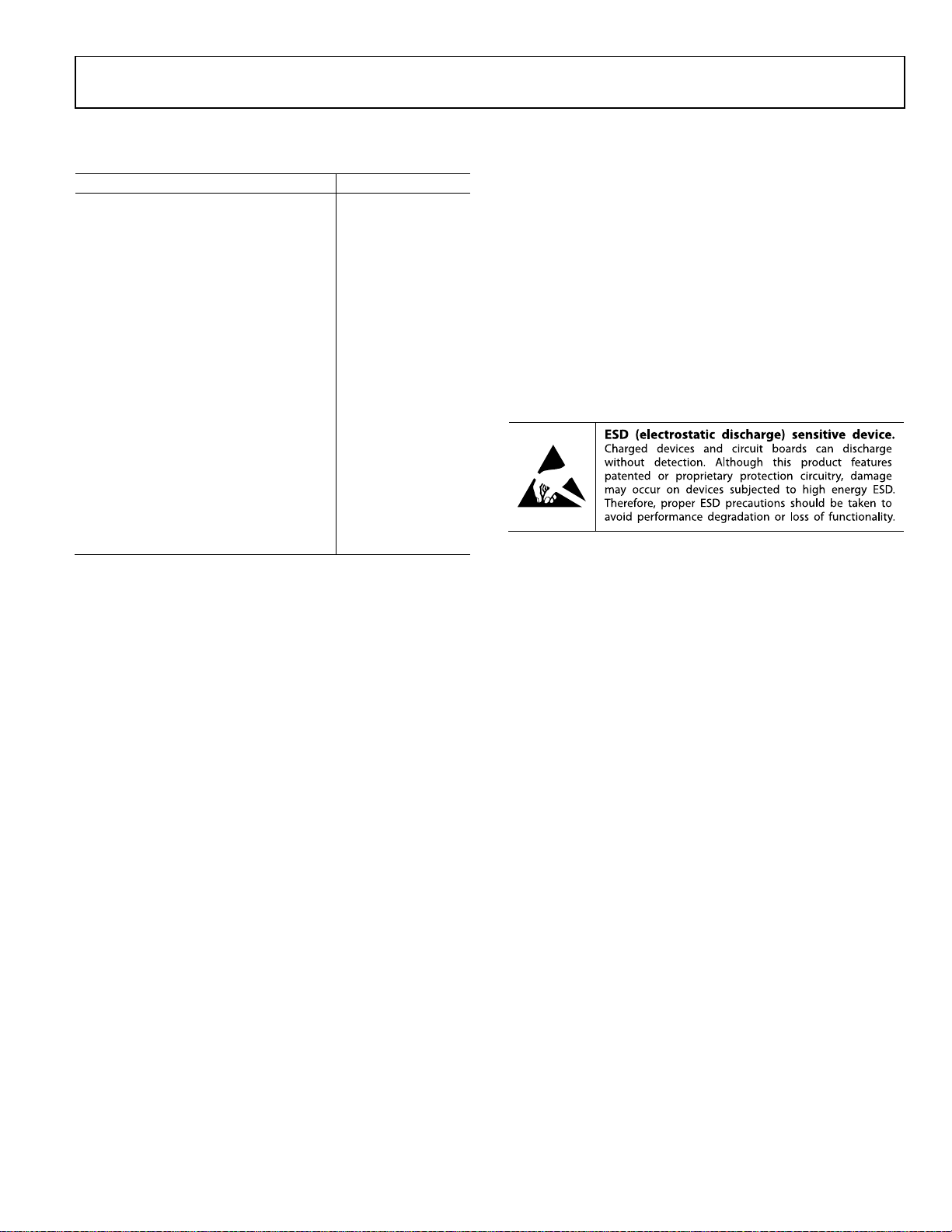
ESD CAUTION
Rev. A | Page 7 of 24
ADP1876 Data Sheet
Enable Input for Channel 1. Drive EN1 high to turn on the Channel 1 controller, and drive it low to turn it off. Tie EN1
to VIN for automatic startup. For a precision UVLO, put an appropriately sized resistor divider from VIN to AGND and
to VIN for automatic startup. For a precision UVLO, put an appropriately sized resistor divider from VIN to AGND and
24
SW1
23
DH1
22
PGND1
21
DL1
20
DL2
19
PGND2
18
DH2
17
SW2
1
2
3
4
5
6
7
8
EN1
VIN
VINLDO
VOUTLDO
VCCO
VDL
AGND
NC
9
10111213141516
EN2
FB2
COMP2
RAMP2
SS2
PGOOD2
ILIM2
BST2
32313029282726
25
TRK1
FB1
COMP1
RAMP1
SS1
PGOOD1
ILIM1
BST1
ADP1876
TOP VIEW
(Not to S cale)
NOTES
1. NC = NO CO NNE C T. DO NOT CONNECT TO THIS PIN.
2. CONNECT THE BOTTOM EXPOSED PAD OF THE
LFCSP PACKAGE TO SYSTEM AGND PLANE .
10103-003
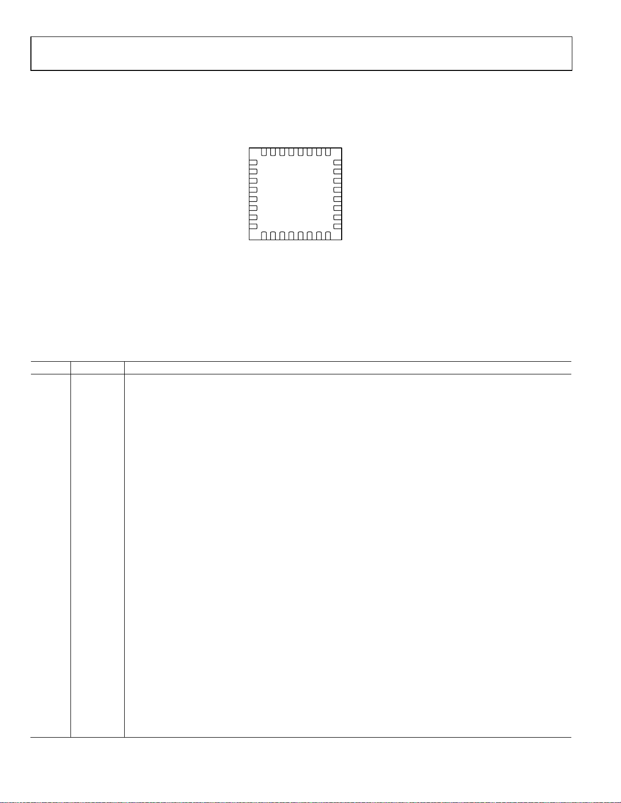
PIN CONFIGURATION AND FUNCTION DESCRIPTIONS
Figure 3. Pin Configuration
Table 3. Pin Function Descriptions
Pin No. Mnemonic Description
1 EN1
tie the midpoint to this pin.
2 VIN Connect to Main Power Supply. Bypass with a 1 μF or larger ceramic capacitor connected as close to this pin as
possible and PGNDx.
3 VINLDO Input for Independent Linear Dropout (LDO) Regulator.
4 VOUTLDO Output for Independent LDO Regulator.
5 VCCO Output of the Internal LDO. The internal circuitry and gate drivers are powered from VCCO. Bypass VCCO to AGND
with a 1 μF or larger ceramic capacitor. The VCCO output is always active, even during fault conditions, and it
cannot be turned off even when EN1 or EN2 is low. For operation at VIN below 5 V, VIN can be jumped to VCCO. Do
not use the VCCO to power any other auxiliary system load.
6 VDL Power Supply for the Low-Side Driver. Bypass VDL to PGNDx with a 1 μF ceramic capacitor. Connect VCCO to VDL.
7 AGND Analog Ground.
8 NC No connect. Do not connect to this pin.
9 EN2 Enable Input for Channel 2. Drive EN2 high to turn on the Channel 2 controller, and drive it low to turn off. Tie EN2
tie the midpoint to this pin.
10 FB2 Output Voltage Feedback for Channel 2.
11 COMP2 Compensation Node for Channel 2. Output of the Channel 2 error amplifier. Connect a series resistor/capacitor
network from COMP2 to AGND to compensate the regulation control loop.
voltage at RAMP2 is 0.2 V during operation. This pin is high impedance when the channel is disabled.
internally pulled up to 3.2 V through a 6.5 µA current source.
PGOOD2 and VCCO. PGOOD2 is pulled to ground when the Channel 2 output is outside the regulation window. An
external pull-up resistor is not required.
the current-limit offset. For accurate current-limit sensing, connect ILIM2 to a current sense resistor at the source of
12 RAMP2 Programmable Current Setting for Slope Compensation of Channel 2. Connect a resistor from RAMP2 to VIN. The
13 SS2 Soft Start Input for Channel 2. Connect a capacitor from SS2 to AGND to set the soft start period. This node is
14 PGOOD2 Open-Drain Power-Good Indicator Logic Output at PGOOD2. An internal 12 kΩ resistor is connected between
15 ILIM2 Current-Limit Sense Comparator Inverting Input for Channel 2. Connect a resistor between ILIM2 and SW2 to set
the low-side MOSFET.
16 BST2 Boot Strapped Upper Rail of High-Side Internal Driver for Channel 2. Connect a 0.1 µF to 0.22 µF multilayer ceramic
capacitor (MLCC) between BST2 and SW2. There is an internal boost rectifier connected between VDL and BST2.
Rev. A | Page 8 of 24
 Loading...