Synchronous Current-Mode with
V
V
Constant On-Time, PWM Buck Controller
FEATURES
Power input voltage as low as 2.75 V to 20 V
Bias supply voltage range: 2.75 V to 5.5 V
Minimum output voltage: 0.6 V
0.6 V reference voltage with ±1.0% accuracy
Supports all N-channel MOSFET power stages
Available in 300 kHz, 600 KHz, and 1.0 MHz options
No current-sense resistor required
Power saving mode (PSM) for light loads (ADP1873 only)
Resistor-programmable current-sense gain
Thermal overload protection
Short-circuit protection
Precision enable input
Integrated bootstrap diode for high-side drive
140 μA shutdown supply current
Starts into a precharged load
Small, 10-lead MSOP package
APPLICATIONS
Telecom and networking systems
Mid to high end servers
Set-top boxes
DSP core power supplies
ADP1872/ADP1873
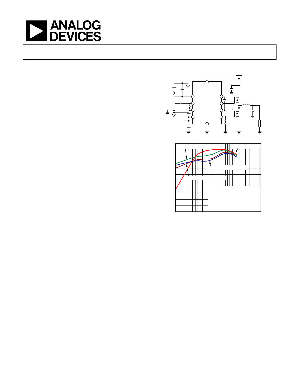
TYPICAL APPLICATIONS CIRCUIT
C
C
C
C2
R
C
R
TOP
V
OUT
R
BOT
C
VDD2
VDD = 2.75V
TO 5.5V
C
VDD
100
= 5.5V, VIN = 5.5V (PSM)
V
DD
95
90
85
80
75
70
65
EFFICIENCY (%)
60
55
50
45
V
DD
100 1k 10k 100k
Figure 2. ADP1872 Efficiency vs. Load Current (V
VIN
ADP1872/
ADP1873
COMP/EN
FB DRVH
GND SW
VDD DRVL
BST
PGND
Figure 1.
= 5.5V, VIN = 13.0V (PS M)
V
DD
= 5.5V, VIN = 16.5V (PSM )
TA = 25°C
V
= 1.8V
OUT
f
= 300kHz
SW
WURTH INDUCTOR:
744325120, L = 1.2µH, DCR = 1.8m
INFINEON FETs:
BSC042N03MS G (UPPER/ LOWER)
LOAD CURRENT (mA)
= 2.75V TO 20
IN
C
IN
C
BST
R
RES
V
= 5.5V, VIN = 5.5V
DD
OUT
Q1
L
V
OUT
+
C
OUT
Q2
LOAD
5A
= 1.8 V, 300 kHz)
08297-001
08297-002
GENERAL DESCRIPTION
The ADP1872/ADP1873 are versatile current-mode, synchronous
step-down controllers that provide superior transient response,
optimal stability, and current limit protection by using a constant
on-time, pseudo-fixed frequency with a programmable currentsense gain, current-control scheme. In addition, these devices offer
optimum performance at low duty cycles by using valley currentmode control architecture. This allows the ADP1872/ADP1873
to drive all N-channel power stages to regulate output voltages
as low as 0.6 V.
The ADP1873 is the power saving mode (PSM) version of the
device and is capable of pulse skipping to maintain output
regulation while achieving improved system efficiency at light
loads (see the Power Saving Mode (PSM) Version (ADP1873)
section for more information).
Rev. A
Information furnished by Analog Devices is believed to be accurate and reliable. However, no
responsibility is assumed by Analog Devices for its use, nor for any infringements of patents or other
rights of third parties that may result from its use. Specifications subject to change without notice. No
license is granted by implication or otherwise under any patent or patent rights of Analog Devices.
Trademarks and registered trademarks are the property of their respective owners.
Available in three frequency options (300 kHz, 600 kHz, and
1.0 MHz, plus the PSM option), the ADP1872/ADP1873 are
well suited for a wide range of applications. These ICs not only
operate from a 2.75 V to 5.5 V bias supply, but can also accept a
power input as high as 20 V.
In addition, an internally fixed, soft start period is included to limit
input in-rush current from the input supply during startup and
to provide reverse current protection during soft start for a precharged output. The low-side current-sense, current-gain scheme
and integration of a boost diode, along with the PSM/forced pulsewidth modulation (PWM) option, reduce the external part count
and improve efficiency.
The ADP1872/ADP1873 operate over the −40°C to +125°C
junction temperature range and are available in a 10-lead MSOP.
One Technology Way, P.O. Box 9106, Norwood, MA 02062-9106, U.S.A.
Tel: 781.329.4700 www.analog.com
Fax: 781.461.3113 ©2009–2010 Analog Devices, Inc. All rights reserved.

ADP1872/ADP1873
TABLE OF CONTENTS
Features .............................................................................................. 1
Applications ....................................................................................... 1
Typical Applications Circuit ............................................................ 1
General Description ......................................................................... 1
Revision History ............................................................................... 2
Specifications ..................................................................................... 3
Absolute Maximum Ratings ............................................................ 5
Thermal Resistance ...................................................................... 5
Boundary Condition .................................................................... 5
ESD Caution .................................................................................. 5
Pin Configuration and Function Descriptions ............................. 6
Typical Performance Characteristics ............................................. 7
ADP1872/ADP1873 Block Digram .............................................. 17
Theory of Operation ...................................................................... 18
Startup .......................................................................................... 18
Soft Start ...................................................................................... 18
Precision Enable Circuitry ........................................................ 18
Undervoltage Lockout ............................................................... 18
Thermal Shutdown ..................................................................... 18
Programming Resistor (RES) Detect Circuit .......................... 19
Valley Current-Limit Setting .................................................... 19
Hiccup Mode During Short Circuit ......................................... 20
Synchronous Rectifier ................................................................ 21
Power Saving Mode (PSM) Version (ADP1873) .................... 21
Timer Operation ........................................................................ 21
Pseudo-Fixed Frequency ........................................................... 22
Applications Information .............................................................. 23
Feedback Resistor Divider ........................................................ 23
Inductor Selection ...................................................................... 23
Output Ripple Voltage (VRR) .................................................. 23
Output Capacitor Selection ....................................................... 23
Compensation Network ............................................................ 24
Efficiency Consideration ........................................................... 25
Input Capacitor Selection .......................................................... 26
Thermal Considerations ............................................................ 27
Design Example .......................................................................... 27
External Component Recommendations .................................... 30
Layout Considerations ................................................................... 32
IC Section (Left Side of Evaluation Board) ............................. 37
Power Section ............................................................................. 37
Differential Sensing .................................................................... 37
Typical Application Circuits ......................................................... 38
Dual-Input, 300 kHz High Current Application Circuit ...... 38
Single-Input, 600 kHz Application Circuit ............................. 38
Dual-Input, 300 kHz High Current Application Circuit ...... 39
Outline Dimensions ....................................................................... 40
Ordering Guide .......................................................................... 40
REVISION HISTORY
3/10—Rev. 0 to Rev. A
Changes to Figure 1 .......................................................................... 1
Changes to Table 1 ............................................................................ 3
Changes to Table 2 ............................................................................ 5
Changes to Figure 59 Caption and Figure 60 Caption .............. 16
Changes to Figure 64 ...................................................................... 17
Changes to Timer Operation Section .......................................... 22
Changes to Table 7 .......................................................................... 23
Changes to Inductor Section ......................................................... 28
Changes to Table 9 .......................................................................... 31
Changes to Figure 82 ...................................................................... 32
Rev. A | Page 2 of 40
Changes to Figure 83 ...................................................................... 33
Changes to Figure 84 ...................................................................... 34
Changes to Figure 85 ...................................................................... 35
Changes to Figure 86 ...................................................................... 36
Changes to Differential Sensing Section and Figure 88 ............ 37
Changes to Figure 89 and Figure 90............................................. 38
Changes to Figure 91 ...................................................................... 39
Updated Outline Dimensions ....................................................... 40
10/09—Revision 0: Initial Version

ADP1872/ADP1873
SPECIFICATIONS
All limits at temperature extremes are guaranteed via correlation using standard statistical quality control (SQC). VDD = 5 V,
BST − SW = 5 V, VIN = 13 V. The specifications are valid for T
Table 1.
Parameter Symbol Conditions Min Typ Max Unit
POWER SUPPLY CHARACTERISTICS
High Input Voltage Range VIN ADP1872ARMZ-0.3/ADP1873ARMZ-0.3 (300 kHz) 2.75 12 20 V
ADP1872ARMZ-0.6/ADP1873ARMZ-0.6 (600 kHz) 2.75 12 20 V
ADP1872ARMZ-1.0/ADP1873ARMZ-1.0 (1.0 MHz) 3.0 12 20 V
Low Input Voltage Range VDD CIN = 1 μF to PGND, CIN = 0.22 μF to GND
ADP1872ARMZ-0.3/ADP1873ARMZ-0.3 (300 kHz) 2.75 5 5.5 V
ADP1872ARMZ-0.6/ADP1873ARMZ-0.6 (600 kHz) 2.75 5 5.5 V
ADP1872ARMZ-1.0/ADP1873ARMZ-1.0 (1.0 MHz) 3.0 5 5.5 V
Quiescent Current I
Shutdown Current I
Q_DD
DD, SD
+ I
FB = 1.5 V, no switching 1.1 mA
Q_BST
+ I
COMP/EN < 285 mV 140 215 μA
BST, SD
Undervoltage Lockout UVLO Rising VDD (See Figure 34 for temperature variation) 2.65 V
UVLO Hysteresis Falling VDD from operational state 190 mV
SOFT START
Soft Start Period See Figure 57 3.0 ms
ERROR AMPLIFER
FB Regulation Voltage VFB T
T
T
= 25°C 600 mV
J
= −40°C to +85°C 595.5 600 605.4 mV
J
= −40°C to +125°C 594.2 600 606.5 mV
J
Transconductance GM 300 515 730 μs
FB Input Leakage Current I
FB = 0.6 V, COMP/EN = released 1 50 nA
FB, LEAK
CURRENT-SENSE AMPLIFIER GAIN
Programming Resistor (RES)
RES = 47 kΩ ± 1% 2.7 3 3.3 V/V
Value from DRVL to PGND
RES = 22 kΩ ± 1% 5.5 6 6.5 V/V
RES = none 11 12 13 V/V
RES = 100 kΩ ± 1% 22 24 26 V/V
SWITCHING FREQUENCY
Typical values measured at 50% time points with
0 nF at DRVH and DRVL; maximum values are
guaranteed by bench evaluation
ADP1872ARMZ-0.3/
300 kHz
ADP1873ARMZ-0.3 (300 kHz)
On-Time VIN = 5 V, V
Minimum On-Time VIN = 20 V 145 190 ns
Minimum Off-Time 84% duty cycle (maximum) 320 385 ns
ADP1872ARMZ-0.6/
600 kHz
ADP1873ARMZ-0.6 (600 kHz)
On-Time VIN = 5 V, V
Minimum On-Time VIN = 20 V, V
Minimum Off-Time 65% duty cycle (maximum) 320 385 ns
ADP1872ARMZ-1.0/
1.0 MHz
ADP1873ARMZ-1.0 (1.0 MHz)
On-Time VIN = 5 V, V
Minimum On-Time VIN = 20 V 60 85 ns
Minimum Off-Time 45% duty cycle (maximum) 320 385 ns
= −40°C to +125°C, unless otherwise specified.
J
1
= 2 V, TJ = 25°C 1120 1200 1280 ns
OUT
= 2 V, TJ = 25°C 500 520 580 ns
OUT
= 0.8 V 82 110 ns
OUT
= 2 V, TJ = 25°C 285 312 340 ns
OUT
Rev. A | Page 3 of 40

ADP1872/ADP1873
Parameter Symbol Conditions Min Typ Max Unit
OUTPUT DRIVER CHARACTERISTICS
High-Side Driver
Output Source Resistance I
Output Sink Resistance I
Rise Time2 t
Fall Time2 t
BST − SW = 4.4 V, CIN = 4.3 nF (see Figure 59) 25 ns
r, DR VH
BST − SW = 4.4 V, CIN = 4.3 nF (see Figure 60) 11 ns
f, DRV H
Low-Side Driver
Output Source Resistance I
Output Sink Resistance I
Rise Time2 t
Fall Time2 t
VDD = 5.0 V, CIN = 4.3 nF (see Figure 60) 18 ns
r, DR VL
VDD = 5.0 V, CIN = 4.3 nF (see Figure 59) 16 ns
f, DRV L
Propagation Delays
DRVL Fall to DRVH Rise2 t
DRVH Fall to DRVL Rise2 t
SW Leakage Current I
BST − SW = 4.4 V (see Figure 59) 22 ns
tpdh, DRVH
BST − SW = 4.4 V (see Figure 60) 24 ns
tpdh, DRVL
BST = 25 V, SW = 20 V, VDD = 5.5 V 110 μA
SW, LEAK
Integrated Rectifier
Channel Impedance I
PRECISION ENABLE THRESHOLD
Logic High Level VIN = 2.9 V to 20 V, VDD = 2.75 V to 5.5 V 235 285 330 mV
Enable Hysteresis VIN = 2.9 V to 20 V, VDD = 2.75 V to 5.5 V 35 mV
COMP VOLTAGE
COMP Clamp Low Voltage V
COMP Clamp High Voltage V
COMP Zero Current Threshold V
THERMAL SHUTDOWN T
COMP (LOW )
COMP (H IGH)
COMP_ZC T
TMSD
(2.75 V ≤ VDD ≤ 5.5 V) 2.55 V
(2.75 V ≤ VDD ≤ 5.5 V) 1.15 V
Thermal Shutdown Threshold Rising temperature 155 °C
Thermal Shutdown Hysteresis 15 °C
Hiccup Current Limit Timing 6 ms
1
The maximum specified values are with the closed loop measured at 10% to 90% time points (see Figure and Figure 60), C
MOSFETs being Infineon BSC042N03MS G.
2
Not automatic test equipment (ATE) tested.
= 1.5 A, 100 ns, positive pulse (0 V to 5 V) 2 3.5 Ω
SOURCE
= 1.5 A, 100 ns, negative pulse (5 V to 0 V) 0.8 2 Ω
SINK
= 1.5 A, 100 ns, positive pulse (0 V to 5 V) 1.7 3 Ω
SOURCE
= 1.5 A, 100 ns, negative pulse (5 V to 0 V) 0.75 2 Ω
SINK
= 10 mA 22 Ω
SINK
From disable state, release COMP/EN pin to enable
0.47 V
device (2.75 V ≤ VDD ≤ 5.5 V)
59
= 4.3 nF and upper- and lower-side
GATE
Rev. A | Page 4 of 40
ADP1872/ADP1873
ABSOLUTE MAXIMUM RATINGS
Table 2.
Parameter Rating
VDD to GND −0.3 V to +6 V
VIN to PGND −0.3 V to +28 V
FB, COMP/EN to GND −0.3 V to (VDD + 0.3 V)
DRVL to PGND −0.3 V to (VDD + 0.3 V)
SW to PGND −0.3 V to +28 V
SW to PGND −2 V pulse (20 ns)
BST to SW −0.6 V to (VDD + 0.3 V)
BST to PGND −0.3 V to +28 V
DRVH to SW −0.3 V to VDD
PGND to GND ±0.3 V
Operating Junction Temperature
Range
Storage Temperature Range −65°C to +150°C
Soldering Conditions JEDEC J-STD-020
Maximum Soldering Lead
Temperature (10 sec)
Stresses above those listed under Absolute Maximum Ratings
may cause permanent damage to the device. This is a stress
rating only; functional operation of the device at these or any
other conditions above those indicated in the operational
section of this specification is not implied. Exposure to absolute
maximum rating conditions for extended periods may affect
device reliability.
−40°C to +125°C
300°C
Absolute maximum ratings apply individually only, not in
combination. Unless otherwise specified, all other voltages are
referenced to PGND.
THERMAL RESISTANCE
θJA is specified for the worst-case conditions, that is, a device
soldered in a circuit board for surface-mount packages.
Table 3. Thermal Resistance
Package Type θJA Unit
θJA (10-Lead MSOP)
2-Layer Board 213.1 °C/W
4-Layer Board 171.7 °C/W
BOUNDARY CONDITION
In determining the values given in Ta b l e 2 and Ta b le 3 , natural
convection was used to transfer heat to a 4-layer evaluation board.
ESD CAUTION
Rev. A | Page 5 of 40

ADP1872/ADP1873
PIN CONFIGURATION AND FUNCTION DESCRIPTIONS
VIN
1
FB
GND
VDD
2
ADP1872
3
TOP VIEW
(Not to Scale)
4
5
COMP/EN
Figure 3. Pin Configuration
Table 4. Pin Function Descriptions
Pin No. Mnemonic Description
1 VIN High Input Voltage. Connect VIN to the drain of the upper-side MOSFET.
2 COMP/EN Output of the Internal Error Amplifier/IC Enable. When this pin functions as EN, applying 0 V to this pin disables the IC.
3 FB Noninverting Input of the Internal Error Amplifier. This is the node where the feedback resistor is connected.
4 GND
Analog Ground Reference Pin of the IC. All sensitive analog components should be connected to this ground
plane (see the Layout Considerations Section).
5 VDD
Bias Voltage Supply for the ADP1872/ADP1873 Controller (Includes the Output Gate Drivers). A bypass capacitor
of 1 μF directly from this pin to PGND and a 0.1 μF across VDD and GND are recommended.
6 DRVL
Drive Output for the External Lower Side, N-Channel MOSFET. This pin also serves as the current-sense gain
setting pin (see Figure 68).
7 PGND Power GND. Ground for the lower side gate driver and lower side, N-channel MOSFET.
8 DRVH Drive Output for the External Upper Side, N-Channel MOSFET.
9 SW Switch Node Connection.
10 BST
Bootstrap for the Upper Side MOSFET Gate Drive Circuitry. An internal boot rectifier (diode) is connected
between VDD and BST. A capacitor from BST to SW is required. An external Schottky diode can also be
connected between VDD and BST for increased gate drive capability.
BST
10
9
SW
8
DRVH
PGND
7
DRVL
6
08297-003
Rev. A | Page 6 of 40
ADP1872/ADP1873
TYPICAL PERFORMANCE CHARACTERISTICS
100
VDD = 5.5V, VIN = 13V (PSM)
95
V
= 5.5V,
DD
V
= 16.5V ( PSM)
IN
90
85
80
VDD = 5.5V,
75
V
= 5.5V
IN
(PSM)
70
65
60
55
EFFICIENCY (%)
50
45
40
35
30
100 100k10k1k
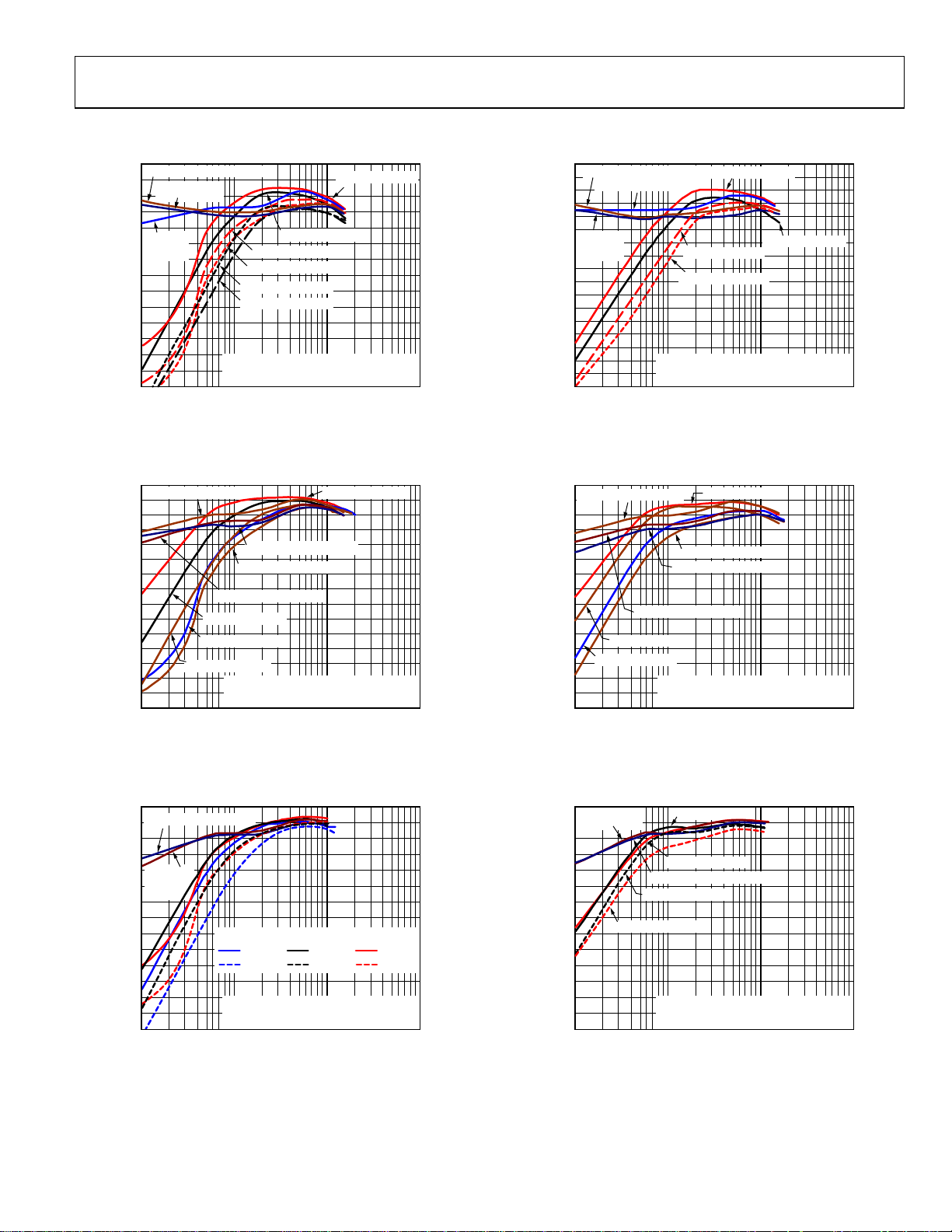
Figure 4. Efficiency—300 kHz, V
V
= 5.5V, VIN = 5.5V
DD
= 3.6V, VIN = 5.5V
V
DD
V
= 5.5V, VIN = 13V
DD
V
= 3.6V, VIN = 13V
DD
V
= 5.5V, VIN = 16.5V
DD
V
= 3.6V, VIN = 16.5V
DD
WURTH IND: 744355147, L = 0.47µH, DCR: 0.80m
INFINEON FETs: BSC042N03MS G (UPPER/LOWER)
TA = 25°C
LOAD CURRENT (mA)
= 0.8 V
OUT
08297-004
100
VDD = 5.5V, VIN = 13V (PSM)
95
V
= 5.5V, VIN = 5.5V (PSM)
DD
90
85
80
75
V
= 5.5V,
DD
70
V
= 16.5V
IN
(PSM)
65
60
55
50
45
EFFICIENCY (%)
40
35
30
25
20
15
100 100k10k1k
Figure 7. Efficiency—600 kHz, V
= 5.5V, VIN = 5.5V
V
DD
V
= 3.6V, VIN = 5.5V
V
= 5.5V, VIN = 13V
DD
V
= 5.5V, VIN = 16.5V
DD
WURTH IND: 744355147, L = 0.47µH, DCR: 0.80m
INFINEON FETs: BSC042N03MS G (UPPER/LOWER)
TA = 25°C
DD
LOAD CURRENT (mA)
= 0.8 V
OUT
08297-007
100
VDD = 5.5V, VIN = 5.5V (PSM)
95
90
85
80
75
70
65
60
55
EFFICIENCY (%)
50
45
40
35
30
25
100 100k10k1k
Figure 5. Efficiency—300 kHz, V
100
VDD = 5.5V, VIN = 16.5V (PSM)
95
90
85
80
= 5.5V,
V
DD
V
= 16V
IN
75
(PSM)
70
65
60
55
EFFICIENCY (%)
50
45
40
35
30
100 100k10k1k
Figure 6. Efficiency—300 kHz, V
V
= 5.5V, VIN = 16.5V ( PSM)
V
DD
V
= 5.5V, VIN = 16.5V
DD
V
= 5.5V, VIN = 13V (PSM)
DD
V
= 3.6V, VIN = 3.6V
DD
V
= 5.5V, VIN = 13V
DD
V
= 3.6V, VIN = 5.5V
DD
WURTH IND: 744325120, L = 1.2µH, DCR: 1.8m
INFINEON FETS: BSC042N03MS G ( UPPER/LOWER)
TA = 25°C
LOAD CURRENT (mA)
OUT
VDD = 2.7V
13V
16.5V
WURTH IND: 7443551200, L = 2µH, DCR: 2.6m
INFINEON FETs: BSC042N03MS G (UPPER/LOWER)
TA = 25°C
LOAD CURRENT (mA)
IN
IN
VDD = 3.6V
13V
16.5V
= 5.5V, VIN = 5.5V
DD
= 1.8 V
VDD = 5.5V
IN
IN
= 7 V
OUT
13V
16.5V
100
VDD = 5.5V, = VIN = 5.5(PSM)
95
VDD = 5.5V, VIN = 5.5V
90
85
80
75
70
VDD = 5.5V, VIN = 16.5V
V
= 5.5V, VIN = 16.5V (PSM)
DD
65
60
55
EFFICIENCY (%)
50
45
V
DD
40
35
30
25
100 100k10k1k
08297-005
= 5.5V, VIN = 13V (PSM)
V
DD
V
= 3.6V, VIN = 5.5V
DD
= 5.5V, VIN = 13V
WURTH IND: 744325120, L = 1.2µH, DCR: 1.8m
INFINEON FETS: BSC042N03MS G ( UPPER/LOWER)
TA = 25°C
LOAD CURRENT (mA)
Figure 8. Efficiency—600 kHz, V
OUT
08297-008
= 1.8 V
100
95
VDD = 5.5V,
V
= 13V (PSM)
IN
VDD = 3.6V,VIN = 13V
90
85
80
75
70
65
60
55
IN
IN
EFFICIENCY (%)
50
V
VDD = 5.5V, VIN = 13V
VDD = 5.5V, VIN = 16.5V (PSM)
VDD = 3.6V, VIN = 16.5V
= 5.5V, VIN = 16.5V
DD
45
40
35
30
100 100k10k1k
08297-006
Figure 9. Efficiency—600 kHz, V
WURTH IND: 7443551200, L = 2µH, DCR: 2.6m
INFINEON FETs: BSC042N03MS G (UPPER/LOWER)
TA = 25°C
LOAD CURRENT (mA)
= 5 V
OUT
08297-009
Rev. A | Page 7 of 40
ADP1872/ADP1873
100
= 5.5V, VIN = 13V (PSM )
V
DD
95
90
85
80
75
= 5.5V,
V
70
DD
V
= 16.5V
IN
65
(PSM)
60
55
50
EFFICIENCY (%)
45
40
35
30
25
20
100 100k10k1k
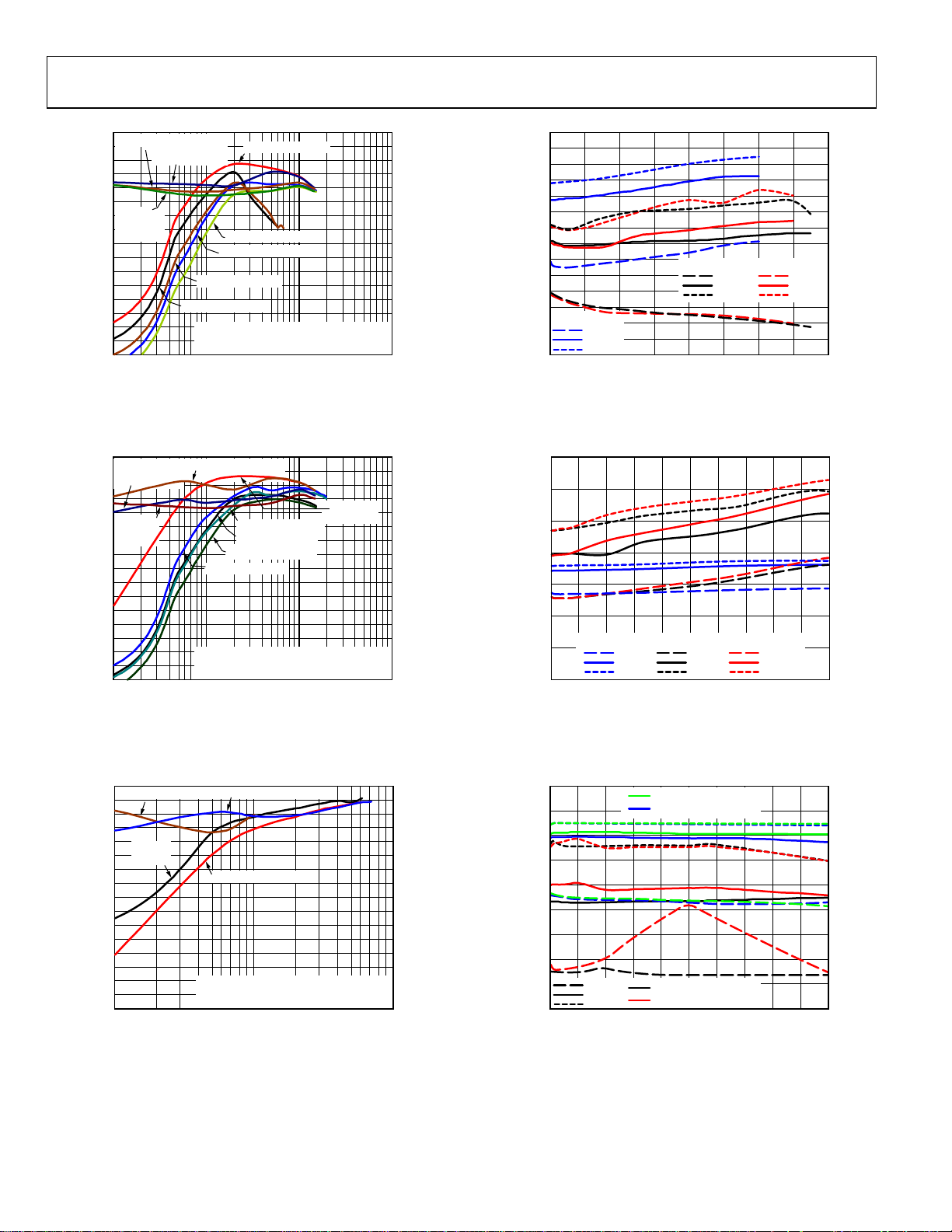
Figure 10. Efficiency—1.0 MHz, V
V
DD
= 5.5V, VIN = 13V
V
DD
= 3.6V, VIN = 5.5V
V
DD
VDD = 5.5V, VIN = 5.5V
= 5.5V, VIN = 16.5V
V
= 5.5V,
DD
V
= 5.5V (PSM)
IN
V
= 3.6V, VIN = 3.6V
DD
WURTH IND: 744303012, L = 0.12µH, DCR: 0.33m
INFINEON FETs: BSC042N03MS G (UPPER/LOWER)
TA = 25°C
LOAD CURRENT (mA)
OUT
08297-010
= 0.8 V
0.8030
0.8025
0.8020
0.8015
0.8010
0.8005
0.8000
0.7995
0.7990
0.7985
OUTPUT VOLTAGE (V)
0.7980
0.7975
0.7970
0.7965
0.7960
VIN = 5.5V
+125°C
+25°C
–40°C
0 2000 4000 6000 8000 10,000 12,000 14, 000 16,000
VIN = 13V
+125°C
+25°C
–40°C
LOAD CURRENT (mA)
Figure 13. Output Voltage Accuracy—300 kHz, V
VIN = 16.5V
+125°C
+25°C
–40°C
= 0.8 V
OUT
08297-013
100
95
90
VDD = 5.5V,
V
= 16.5V (PSM)
IN
= 5.5V, VIN = 5V (PSM )
V
DD
85
80
= 5.5V,
V
DD
75
V
= 13V
IN
(PSM)
70
65
60
55
50
EFFICIENCY (%)
45
40
35
30
25
20
100 100k10k1k
WURTH IND: 744303022, L = 0.22µH, DCR: 0.33m
INFINEON FETs: BSC042N03MS G (UPPER/LOWER)
TA = 25°C
Figure 11. Efficiency—1.0 MHz, V
100
VDD = 5.5V, VIN = 5V (PSM)
95
90
85
80
75
70
= 5V,
V
DD
V
= 13V
IN
65
60
55
50
EFFICIENCY (%)
45
40
35
30
25
20
100 10k1k
WURTH IND: 744325072, L = 0.72µH, DCR: 1.65m
INFINEON FETs: BSC042N03MS G (UPPER/LOWER)
TA = 25°C
Figure 12. Efficiency—1.0 MHz, V
= 5.5V, VIN = 16.5V
V
DD
VDD = 3.6V, VIN = 13V
V
= 3.6V, VIN = 16.5V
DD
V
= 5.5V, VIN = 13V
DD
LOAD CURRENT (mA)
= 5.5V, VIN = 16.5V (PSM)
V
DD
V
= 5V, VIN = 16.5V
DD
LOAD CURRENT (mA)
OUT
OUT
V
DD
V
IN
= 1.8 V
= 4 V
= 5.5V,
= 5V
1.821
1.816
1.811
1.806
1.801
OUTPUT VOLTAGE (V)
1.796
1.791
1.786
08297-011
VIN = 5.5V
+125°C
+25°C
–40°C
0 1500 3000 4500 6000 7500 9000 10,500 12,000 13,500 15,000
Figure 14. Output Voltage Accuracy—300 kHz, V
7.000
6.995
VIN = 13V
+125°C
+25°C
–40°C
LOAD CURRENT (mA)
VDD = 3.6V, VIN = 13V
VDD = 3.6V, VIN = 16.5V
VIN = 16.5V
+125°C
+25°C
–40°C
OUT
08297-014
= 1.8 V
6.990
6.985
6.980
6.975
6.970
OUTPUT VOLTAGE (V)
6.965
6.960
6.955
08297-012
Figure 15. Output Voltage Accuracy—300 kHz, V
+125°C
+25°C
–40°C
VDD = 5.5V, VIN = 13V
VDD = 5.5V, VIN = 16.5V
0 1000 2000 3000 4000 5000 6000 7000 8000 9000 10,000
LOAD CURRENT (mA)
= 7 V
OUT
08297-015
Rev. A | Page 8 of 40
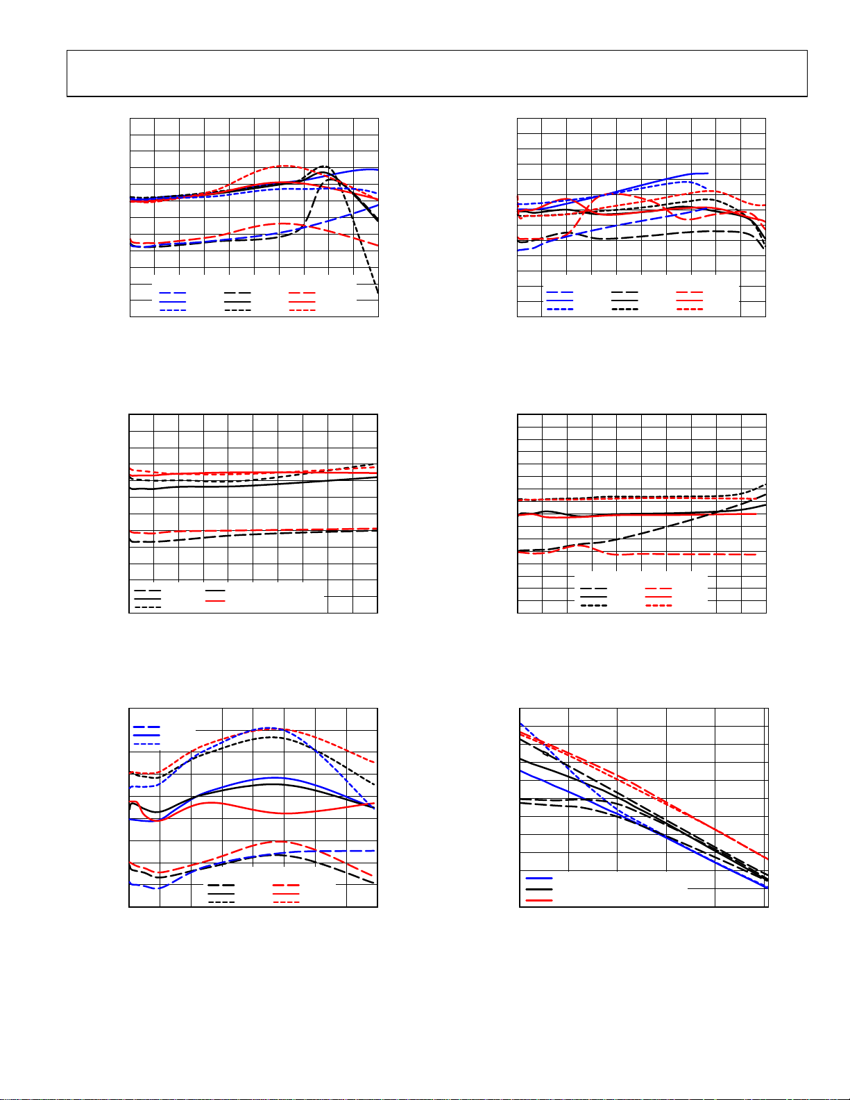
ADP1872/ADP1873
1.801
1.800
1.799
1.798
1.797
1.796
1.795
1.794
1.793
OUTPUT VOLTAGE (V)
1.792
1.791
1.790
1.789
VIN = 5.5V
+125°C
+25°C
–40°C
0 1500 3000 4500 6000 7500 9000 10,500 12,000 13,500 15,000
VIN = 13V
+125°C
+25°C
–40°C
LOAD CURRENT (mA)
VIN = 16.5V
Figure 16. Output Voltage Accuracy—600 kHz, V
+125°C
+25°C
–40°C
OUT
08297-016
= 1.8 V
1.810
1.809
1.808
1.807
1.806
1.805
1.804
1.803
1.802
1.801
OUTPUT VOLTAGE (V)
1.800
1.799
1.798
1.797
VIN = 5.5V
+125°C
+25°C
–40°C
0 1500 3000 4500 6000 7500 9000 10,500 12,000 13,500 15,000
VIN = 13V
+125°C
+25°C
–40°C
LOAD CURRENT (mA)
VIN = 16.5V
Figure 19. Output Voltage Accuracy—1.0 MHz, V
+125°C
+25°C
–40°C
OUT
= 1.8 V
08297-019
5.044
5.042
5.040
5.038
5.036
5.034
5.032
5.030
5.028
OUTPUT VOLTAGE (V)
5.026
5.024
5.022
5.020
+125°C
+25°C
–40°C
0 1000 2000 3000 4000 5000 6000 7000 8000 9000 10,000
VDD = 5.5V, VIN = 13V
VDD = 5.5V, VIN = 16.5V
LOAD CURRENT (mA)
Figure 17. Output Voltage Accuracy—600 kHz, V
0.807
VIN = 5.5V
0.806
0.805
0.804
0.803
0.802
0.801
OUTPUT VOLTAGE (V)
0.800
0.799
0.798
+125°C
+25°C
–40°C
VIN = 13V
0 2000 4000 6000 8000 10,000 12,000 14,000 16,000
LOAD CURRENT (mA)
+125°C
+25°C
–40°C
VIN = 16.5V
+125°C
+25°C
–40°C
Figure 18. Output Voltage Accuracy—1 MHz, V
OUT
OUT
= 5 V
= 0.8 V
4.050
4.045
4.040
4.035
4.030
4.025
4.020
4.015
4.010
4.005
4.000
3.995
OUTPUT VOLTAGE (V)
3.990
3.985
3.980
3.975
3.970
0 800 1600 2400 3200 4000 4800 5600 6400 7200 8000
08297-017
Figure 20. Output Voltage Accuracy—1.0 MHz, V
0.6030
0.6025
0.6020
0.6015
0.6010
0.6005
0.6000
0.5995
0.5990
FEEDBACK VOLT AGE (V)
0.5985
0.5980
0.5975
–40.0 –7. 5 122.590.057.525.0
08297-018
VIN = 13V
+125°C
+25°C
–40°C
LOAD CURRENT (mA)
VDD = 2.7V, VIN = 2.7V, 3.6V
VDD = 3.6V, VIN = 3.6V TO 16.5V
VDD = 5.5V, VIN = 5.5V, 13V, 16.5V
TEMPERATURE (° C)
VIN = 16.5V
+125°C
+25°C
–40°C
OUT
08297-020
= 4 V
08297-021
Figure 21. Feedback Voltage vs. Temperature
Rev. A | Page 9 of 40
ADP1872/ADP1873
335
325
315
305
295
285
275
265
FREQUENCY (kHz)
255
245
235
225
10.8 11. 0 11.2 11.4 11.6 11.8 12.0 12.2 12.4 12.6 12.8 13.0 13.2
VDD = 3.6V
+125°C
+25°C
–40°C
VIN (V)
NO LOADVDD = 5.5V
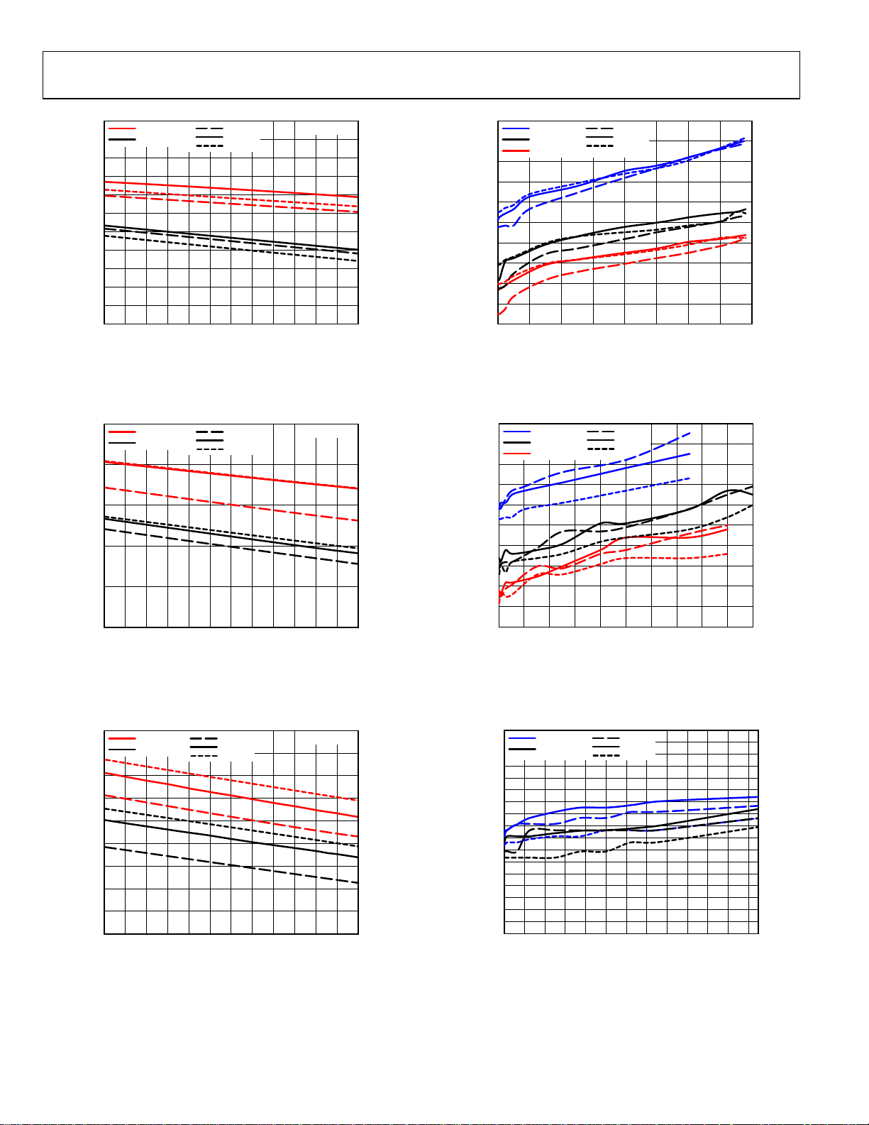
Figure 22. Switching Frequency vs. High Input Voltage,
300 kHz, ±10% of 12 V
08297-022
340
325
310
295
280
265
250
FREQUENCY (kHz)
235
220
205
190
0 1 6,00014,00012,00010,0008000600040002000
VIN = 5.5V
VIN = 13V
VIN = 16.5V
+125°C
+25°C
–40°C
LOAD CURRENT (mA)
Figure 25. Frequency vs. Load Current, 300 kHz, V
OUT
08297-025
= 0.8 V
650
600
550
500
FREQUENCY (kHz)
450
400
10.8 11. 0 11.2 11.4 11.6 11.8 12.0 12.2 12.4 12.6 12.8 13.0 13.2
VDD = 5.5V
VDD = 3.6V
+125°C
+25°C
–40°C
VIN (V)
NO LOAD
Figure 23. Switching Frequency vs. High Input Voltage,
600 kHz, V
1000
950
900
850
800
750
700
FREQUENCY (kHz)
650
600
550
10.8 11. 0 11.2 11.4 11.6 11.8 12.0 12.2 12.4 12.6 12.8 13.0 13.2
VDD = 5.5V
VDD = 3.6V
= 1.8 V, ±10% of 12 V
OUT
+125°C
+25°C
–40°C
VIN (V)
NO LOAD
Figure 24. Switching Frequency vs. High Input Voltage,
1.0 MHz, ±10% of 12 V
360
350
340
330
320
310
300
FREQUENCY (kHz)
290
280
270
260
08297-023
Figure 26. Frequency vs. Load Current, 300 kHz, V
358
354
350
346
342
338
334
330
326
322
318
314
FREQUENCY (kHz)
310
306
302
298
294
290
08297-024
Figure 27. Frequency vs. Load Current, 300 kHz, V
0 20,00016,000 18,00014,00012,00010,0008000600040002000
0 96006400 7200 8000 8800560048004000320024001600800
VIN = 5.5V
VIN = 13V
VIN = 16.5V
VIN = 13V
VIN = 16.5V
+125°C
+25°C
–40°C
LOAD CURRENT (mA)
+125°C
+25°C
–40°C
LOAD CURRENT (mA)
OUT
OUT
= 1.8 V
= 7 V
08297-026
08297-027
Rev. A | Page 10 of 40
ADP1872/ADP1873
700
670
640
610
580
550
520
490
460
430
400
370
FREQUENCY (kHz)
340
310
280
250
220
190
0 16,00014,00012,00010,0008000600040002000
VIN = 5.5V
VIN = 13V
VIN = 16.5V
+125°C
+25°C
–40°C
LOAD CURRENT (mA)
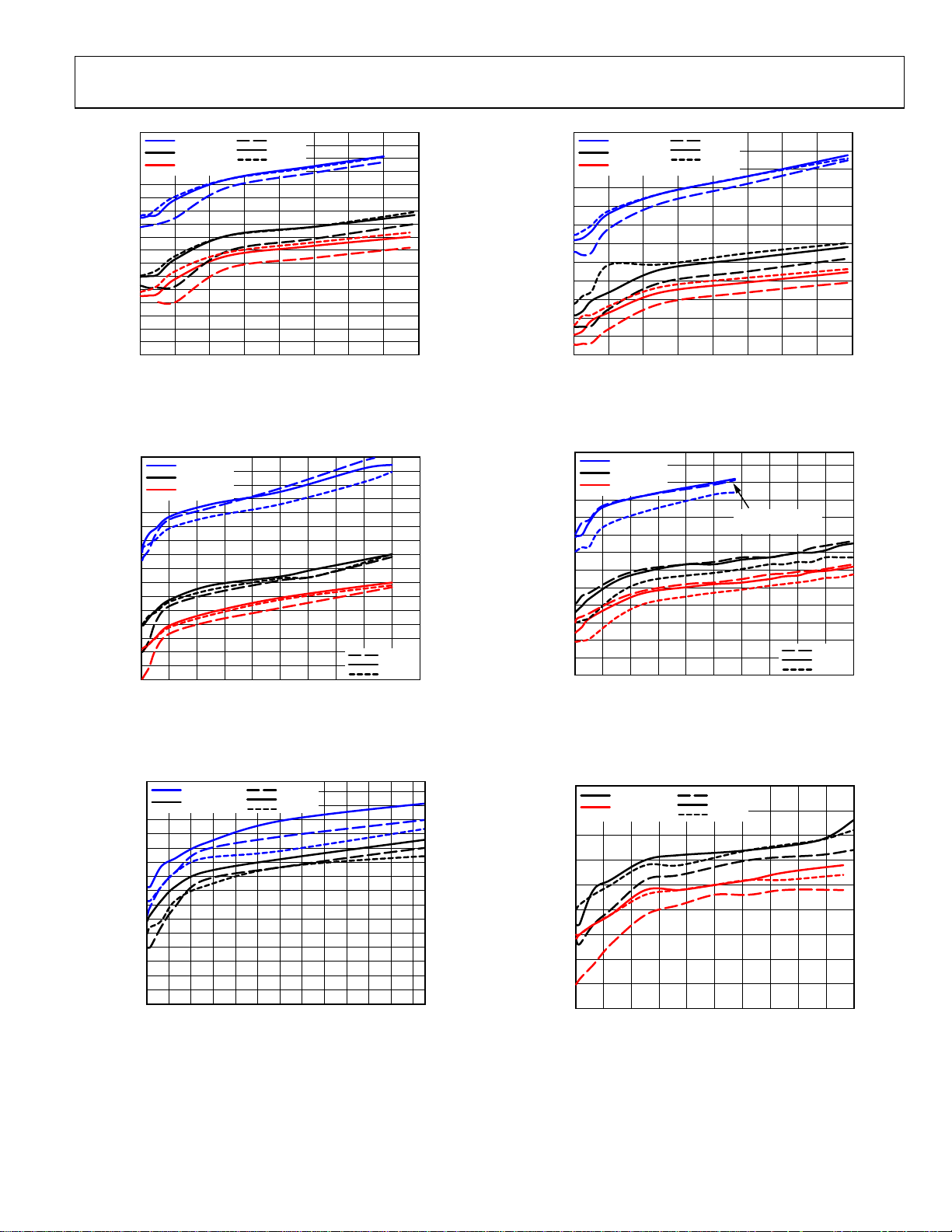
Figure 28. Frequency vs. Load Current, 600 kHz, V
= 0.8 V
OUT
08297-028
FREQUENCY (kHz)
1300
1125
1150
1075
1000
925
850
775
700
625
550
475
400
0 16,00014,00012,00010,0008000600040002000
VIN = 5.5V
VIN = 13V
VIN = 16.5V
+125°C
+25°C
–40°C
LOAD CURRENT (mA)
Figure 31. Frequency vs. Load Current, V
= 1.0 MHz, 0.8 V
OUT
08297-031
815
795
775
755
735
715
695
675
655
635
615
FREQUENCY (kHz)
595
575
555
535
515
495
0 20,00016,000 18,00014,00012,00010,0008000600040002000
VIN = 5.5V
VIN = 13V
VIN = 16.5V
LOAD CURRENT (mA)
Figure 29. Frequency vs. Load Current, 600 kHz, V
0 96008800800072006400560048004000320024001600800
VIN = 13V
VIN = 16.5V
705
698
691
684
677
670
663
656
649
642
FREQUENCY (kHz)
635
628
621
614
607
600
+125°C
+25°C
–40°C
LOAD CURRENT (mA)
Figure 30. Frequency vs. Load Current, 600 kHz, V
+125°C
+25°C
–40°C
= 1.8 V
OUT
OUT
=5 V
1450
1375
1300
1225
1150
1075
1000
925
FREQUENCY (kHz)
850
775
700
625
550
08297-029
Figure 32. Frequency vs. Load Current, 1.0 MHz, V
1450
1400
1350
1300
1250
1200
1150
FREQUENCY (kHz)
1100
1050
1000
08297-030
Figure 33. Frequency vs. Load Current, 1.0 MHz, V
VIN = 5.5V
VIN = 13V
VIN = 16.5V
MIN-OFF TIME
ENCROACHMENT
+125°C
+25°C
–40°C
0 20,00016,000 18,00014,00012,00010,0008000600040002000
VIN = 13V +125°C
VIN = 16.5V
0 8000800 1600 2400 3200 4000 4800 5600 6400 7200
LOAD CURRENT (mA)
+25°C
–40°C
LOAD CURRENT (mA)
OUT
OUT
= 1.8 V
= 4 V
08297-032
08297-033
Rev. A | Page 11 of 40
ADP1872/ADP1873
UVLO (V)
2.658
2.657
2.656
2.655
2.654
2.653
2.652
2.651
2.650
2.649
–40 120100806040200–20
TEMPERATURE ( °C)
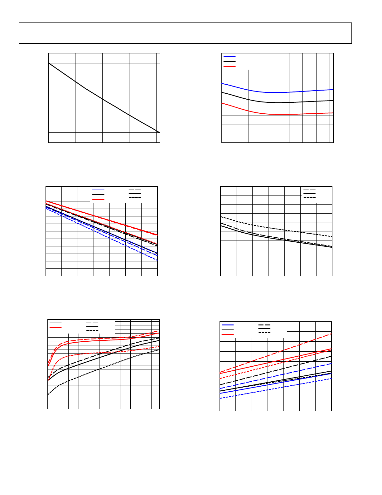
Figure 34. UVLO vs. Temperature
08297-034
680
630
580
530
480
430
380
330
MINIMUM OFF-TIME (ns)
280
230
180
–40 120100806040200–20
VDD = 2.7V
VDD = 3.6V
VDD = 5.5V
TEMPERATURE (° C)
Figure 37. Minimum Off-Time vs. Temperature
08297-037
100
95
90
85
80
75
70
65
60
55
MAXIMUM DUTY CYCLE (%)
50
45
40
300 400 500 600 700 800 900 1000
FREQUENCY (kHz)
VDD = 2.7V
VDD = 3.6V
VDD = 5.5V
Figure 35. Maximum Duty Cycle vs. Frequency
84
82
80
78
76
74
72
70
68
66
64
62
60
58
56
54
52
MAXIMUM DUTY CYCLE (%)
50
48
46
44
42
40
3.6 4. 8 6. 0 7.2 8.4 9.6 10.8 12.0 13.2 14.4 15. 6
VDD = 3.6V +125°C
VDD = 5.5V
+25°C
–40°C
VIN (V)
Figure 36. Maximum Duty Cycle vs. High Voltage Input (VIN)
+125°C
+25°C
–40°C
680
630
580
530
480
430
380
330
MINIMUM OFF-TIME (ns)
280
230
180
2.7 5.55.14.74.33.93.53.1
08297-035
VDD (V)
+125°C
+25°C
–40°C
08297-038
Figure 38. Minimum Off-Time vs. VDD (Low Input Voltage)
800
720
640
560
480
400
320
RECTIFIER DROP (mV)
240
160
80
08297-036
300 400 500 600 700 800 900 1000
VDD = 2.7V
VDD = 3.6V
VDD = 5.5V
+125°C
+25°C
–40°C
FREQUENCY (kHz)
08297-039
Figure 39. Internal Rectifier Drop vs. Frequency
Rev. A | Page 12 of 40
 Loading...