

Constant Frequency Current-Mode
www.BDTIC.com/ADI
FEATURES
Wide input voltage range: 3.15 V to 14 V
Wide output voltage range: 0.8 V to input voltage
Pin-to-pin compatible with LTC1772, LTC3801
Up to 94% efficiency
0.8 V ± 1.25% reference accuracy over temperature
Internal soft start
100% duty cycle for low dropout voltage
Current-mode operation for good line and load
transient response
7 μA shutdown supply current
235 μA quiescent supply current
Short-circuit and overvoltage protection
Small 6-lead TSOT package
APPLICATIONS
Wireless devices
1- to 3-cell Li-Ion battery-powered applications
Set-top boxes
Processor core power supplies
Hard disk drives
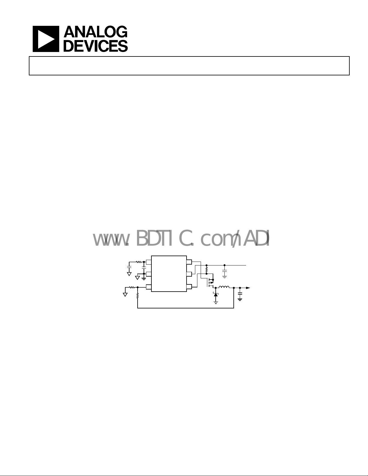
Step-Down DC-to-DC Controller in TSOT
ADP1864
GENERAL DESCRIPTION
The ADP1864 is a compact, inexpensive, constant-frequency,
current-mode, step-down dc-to-dc controller. The ADP1864
drives a P-channel MOSFET that regulates an output voltage as
low as 0.8 V with ±1.25% accuracy, for up to 5 A load currents,
from input voltages as high as 14 V.
The ADP1864 provides system flexibility by allowing accurate
setting of the current limit with an external resistor, and the
output voltage is easily adjustable using two external resistors.
The ADP1864 includes an internal soft start to allow quick
power-up while preventing input inrush current. Additional
safety features include short-circuit protection, output overvoltage
protection, and input undervoltage protection. Current-mode
control provides fast and stable load transient performance,
while the 580 kHz operating frequency allows a small inductor
to be used in the system. To further the life of a battery source,
the controller turns on the external P-channel MOSFET 100%
of the duty cycle during dropout.
The ADP1864 operates over the −40°C to +125°C temperature
range and is available in a small, low profile, 6-lead TSOT package.
TYPICAL APPLICATIONS DIAGRAM
25kΩ
470pF
68pF
80.6kΩ
174kΩ
1
2
3
COMP
ADP1864
GND
FB
PGATE
CS
6
5
IN
4
Figure 1.
0.03Ω
= 3.15V TO 14V
V
IN
10µF
5µH
2.5V, 2.0A
47µF
05562-001
Rev. B
Information furnished by Analog Devices is believed to be accurate and reliable. However, no
responsibility is assumed by Analog Devices for its use, nor for any infringements of patents or other
rights of third parties that may result from its use. Specifications subject to change without notice. No
license is granted by implication or otherwise under any patent or patent rights of Analog Devices.
Trademarks and registered trademarks are the property of their respective owners.
One Technology Way, P.O. Box 9106, Norwood, MA 02062-9106, U.S.A.
Tel: 781.329.4700 www.analog.com
Fax: 781.461.3113 ©2005–2008 Analog Devices, Inc. All rights reserved.

ADP1864
www.BDTIC.com/ADI
TABLE OF CONTENTS
Features .............................................................................................. 1
Applications ....................................................................................... 1
General Description ......................................................................... 1
Typical Applications Diagram ........................................................ 1
Revision History ............................................................................... 2
Specifications ..................................................................................... 3
Absolute Maximum Ratings ............................................................ 4
ESD Caution .................................................................................. 4
Pin Configuration and Function Descriptions ............................. 5
Typical Performance Characteristics ............................................. 6
Theory of Operation ........................................................................ 8
Loop Startup .................................................................................. 8
Short-Circuit Protection .............................................................. 9
Undervoltage Lockout (UVLO) ................................................. 9
Overvoltage Lockout Protection (OVP).................................... 9
Soft Start .........................................................................................9
Applications Information .............................................................. 10
Duty Cycle ................................................................................... 10
Ripple Current ............................................................................ 10
Sense Resistor.............................................................................. 10
Inductor Value ............................................................................ 10
MOSFET ...................................................................................... 11
Diode ............................................................................................ 11
Input Capacitor ........................................................................... 11
Output Capacitor ........................................................................ 11
Feedback Resistors ..................................................................... 11
Layout Considerations ................................................................... 12
Example Applications Circuits ..................................................... 13
Outline Dimensions ....................................................................... 14
Ordering Guide .......................................................................... 14
REVISION HISTORY
4/08—Rev. A to Rev. B
Change General Description Section ............................................. 1
Deleted Figure 2 ................................................................................ 1
Change to FB Regulation Voltage Parameter ................................ 3
Change to MOSFET Section ......................................................... 11
Changes to Ordering Guide .......................................................... 14
2/07—Rev 0. to Rev. A
Updated Format .................................................................. Universal
Changes to Figure 1 .......................................................................... 1
Changes to General Description .................................................... 2
Changes to Specifications ................................................................ 3
Change to Figure 13 ......................................................................... 8
Replaced Layout Considerations Section .................................... 12
Replaced Example Applications Circuits Section ...................... 13
10/05—Revision 0: Initial Version
Rev. B | Page 2 of 16
ADP1864
www.BDTIC.com/ADI
SPECIFICATIONS
VIN = 5 V, TJ = 25°C, unless otherwise noted.
Table 1.
Parameter Symbol Conditions Min Typ Max Unit
POWER SUPPLY
Input Voltage VIN 3.15 14 V
Quiescent Current IQ V
Shutdown Supply Current ISD V
Undervoltage Lockout Threshold V
V
UVLO
V
ERROR AMPLIFIER
FB Input Current IFB V
V
Amplifier Transconductance VFB = 0.8 V, I
COMP Startup Threshold VIN = 3.15 V to 14 V, TJ = −40°C to +125°C 0.55 0.67 0.80 V
COMP Shutdown Threshold VIN = 3.15 V to 14 V, TJ = −40°C to +125°C 0.15 0.3 0.55 V
COMP Start-Up Current Source COMP = GND 0.25 0.6 0.95 μA
FB Regulation Voltage VIN = 3.15 V to 14 V, TJ = −40°C to +125°C 0.790 0.8 0.810 V
Overvoltage Protection Threshold V
Measured at FB, TJ = −40°C to +125°C 0.87 0.885 0.9 V
OVP
Overvoltage Protection Hysteresis 50 mV
CURRENT SENSE
Peak Current Sense Voltage TJ = −40°C to +125°C 90 125 mV
V
Current Sense Gain VCS to V
OUTPUT REGULATION
Line Regulation
Load Regulation
1
V
2
V
OSCILLATOR
Oscillator Frequency VFB = 0.8 V, TJ = −40°C to +125°C 500 580 650 kHz
V
FB Frequency Foldback Threshold 0.35 V
GATE DRIVE
Gate Rise Time C
Gate Fall Time C
Minimum On Time PGATE minimum low duration 190 ns
SOFT START POWER-ON TIME 1.1 ms
1
Line regulation is measured using the application circuit in . Line regulation is specified as the change in the FB voltage resulting from a 1 V change in
the IN voltage.
2
Load regulation is measured using the application circuit in . Load regulation is specified as the change in the FB voltage resulting from a 1 V change in the
COMP voltage. The COMP voltage range is typically 0.9 V to 2.3 V for the minimum to maximum load current condition.
= 3.15 V to 14 V, PGATE = IN 235 360 μA
IN
= 3.15 V to 14 V, COMP = GND 7 15 μA
IN
falling, TJ = −40°C to +125°C 2.75 2.90 3.01 V
IN
rising, TJ = −40°C to +125°C 2.85 3.00 3.15 V
IN
= 0.8 V, TJ = 25°C −20 −2 +20 nA
FB
= 0.8 V, TJ = −40°C to +125°C −40 −2 +40 nA
FB
= ±5 μA 0.24 mmho
COMP
= 3.15 V to 14 V, TJ = −40°C to +125°C 70 125 mV
IN
12 V/V
COMP
= 3.15 V to 14 V, VFB/VIN 0.12 mV/V
IN
−2 mV/V
FB/VCOMP
= 0 V 190 kHz
FB
= 3 nF 50 ns
GATE
= 3 nF 40 ns
GATE
Figure 1
Figure 1
Rev. B | Page 3 of 16
ADP1864
www.BDTIC.com/ADI
ABSOLUTE MAXIMUM RATINGS
Table 2.
Parameter Rating
IN to GND −0.3 V to +16 V
CS, PGATE to GND −0.3 V to (VIN + 0.3 V)
FB, COMP to GND −0.3 V to +6 V
θJA 2-Layer (SEMI Standard Board) 315°C/W
θJA 4-Layer (JEDEC Standard Board) 186°C/W
Operating Junction Temperature Range −40°C to +125°C
Storage Temperature Range −65°C to +150°C
Lead Temperature
Rework Temperature (J-STD-020B) 260°C
Peak Reflow Temperature,
(20 sec to 40 sec, J-STD-020B)
260°C
Stresses above those listed under Absolute Maximum Ratings
may cause permanent damage to the device. This is a stress
rating only; functional operation of the device at these or any
other conditions above those indicated in the operational
section of this specification is not implied. Exposure to absolute
maximum rating conditions for extended periods may affect
device reliability.
ESD CAUTION
Rev. B | Page 4 of 16
ADP1864
www.BDTIC.com/ADI
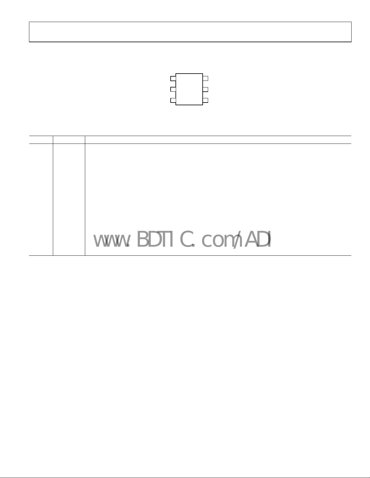
PIN CONFIGURATION AND FUNCTION DESCRIPTIONS
PGATE
6
5
IN
4
CS
05562-003
Table 3. Pin Function Descriptions
Pin No. Mnemonic Description
1 COMP
Regulator Compensation Node. COMP is the output of the internal transconductance error amplifier. Connect a
series RC from COMP to GND to compensate for the control loop. Add an extra high frequency capacitor between
COMP and GND to further reduce switching jitter. The value of this is typically one-tenth of the main compensation
capacitor. Pulling the COMP pin below 0.3 V disables the ADP1864 and turns off the external PFET.
2 GND
Analog Ground. Directly connect the compensation and feedback networks to GND, preferably with a small analog
GND plane. Connect GND to the power ground (PGND) plane with a narrow track at a single point close to the GND
pin. See the Layout Considerations section for more information.
3 FB
Feedback Input. Connect a resistive voltage divider from the output voltage to FB to set the output voltage. The
regulation feedback voltage is 0.8 V. Place the feedback resistors as close as possible to the FB pin.
4 CS
Current Sense Input. CS is the negative input of the current sense amplifier. It provides the current feedback signal
used to terminate the PWM on time. Place a current sense resistor between IN and CS to set the current limit. The
current limit threshold is typically 125 mV.
5 IN
Power Input. IN is the power supply to the ADP1864 and the positive input of the current sense amplifier. Connect
IN to the positive side of the input voltage source. Bypass IN to PGND with a 10 μF or larger capacitor as close as possible
to the ADP1864. For additional high frequency noise reduction, add a 0.1 μF capacitor to PGND at the IN pin.
6 PGATE
Gate Drive Output. PGATE drives the gate of the external P-channel MOSFET. Connect PGATE to the gate of the
external MOSFET.
COMP
1
ADP1864
2
GND
TOP VIEW
(Not to Scale)
3
FB
Figure 2. Pin Configuration
Rev. B | Page 5 of 16

ADP1864
www.BDTIC.com/ADI
TYPICAL PERFORMANCE CHARACTERISTICS
0.810
VIN = 5V
0.805
0.8
0.7
0.6
0.5
COMP RISING
0.800
0.795
REFERENCE VO LTAGE (V)
0.790
–40 –20 0 20 40 60 10080 120
TEMPERATURE (°C)
Figure 3. Reference Voltage vs. Temperature
600
VIN = 5V
590
580
570
FREQUENCY (kHz)
560
550
–40 –20 0 20 40 60 10080 120
TEMPERATURE (°C)
Figure 4. Normalized Oscillator Frequency vs. Temperature
0.4
COMP (V)
0.3
0.2
0.1
05562-004
0
–40 –20 0 20 40 60 10080 120
TEMPERATURE (°C)
COMP FALLING
05562-007
Figure 6. COMP Shutdown Threshold vs. Temperature
2.52
2.50
2.48
(V)
2.46
OUT
V
2.44
2.42
05562-005
2.40
03
0.51.01.52.02.53.0
LOAD (A)
05562-008
.5
Figure 7. Typical Load Regulation (VIN = 5 V; See Figure 1)
3.10
3.05
3.00
2.95
(V)
2.90
IN
V
2.85
2.80
2.75
2.70
–40 –20 0 20 40 60 10080 120
UVLO FALLING
Figure 5. UVLO Voltage vs. Temperature (V
UVLO RI SING
TEMPERATURE ( °C)
Rising and VIN Falling)
IN
05562-006
Rev. B | Page 6 of 16
2.520
2.515
(V)
2.510
OUT
V
2.505
2.500
35791113
VIN (V)
Figure 8. Typical Line Regulation vs. Input Voltage (See Figure 19)
05562-009

ADP1864
www.BDTIC.com/ADI
12
11
10
9
8
7
SHUTDOWN SUPPL Y CURRENT (µA)
6
5
–40 –20 0 20 40 60 10080 120
VIN = 4V
TEMPERATURE (° C)
VIN = 16V
VIN = 5V
VIN = 3.15V
Figure 9. Shutdown Supply Current vs. Temperature
310
290
270
(µA)
250
Q
I
230
210
VIN = 12V
VIN = 5V
VIN = 16V
VIN = 7V
VIN = 4V
VIN = 3.1V
05562-010
650
TEMPERATURE = 25°C
640
630
620
610
600
590
580
570
560
550
FREQUENCY (kHz)
540
530
520
510
500
357 1191
VIN (V)
3
Figure 11. Oscillator Frequency vs. Input Voltage
05562-012
190
–40 –20 0 20 40 60 10080 120
TEMPERATURE ( °C)
05562-011
Figure 10. Quiescent Current vs. Temperature
Rev. B | Page 7 of 16

ADP1864
V
V
www.BDTIC.com/ADI
THEORY OF OPERATION
The ADP1864 is a constant frequency (580 kHz), current-mode
buck controller. PGATE drives the gate of the external P-channel
FET. The duty cycle of the external FET dictates the output
voltage and the current supplied to the load.
The peak inductor current is measured across the external sense
resistor, while the system output voltage is fed back through an
external resistor divider to the FB pin.
At the start of every oscillator cycle, PGATE turns on the
external FET, causing the inductor current, and therefore the
current sense amplifier voltage, to increase. The inductor
current increases until the current amplifier voltage equals
the voltage at the COMP pin. This resets the internal flip-flop,
causing PGATE to go high and turning off the external FET.
The inductor current decreases until the beginning of the next
oscillator period.
The voltage at the COMP node is the output of the internal
error amplifier. The negative input of the error amplifier is the
output voltage scaled by an external resistive divider, and the
= 3.15V TO 14
IN
CSIN
5 4
positive input to the error amplifier is driven by a 0.8 V band
gap reference. An increase in the load current causes a small
drop in the feedback voltage, in turn causing an increase in the
COMP voltage and, therefore, the duty cycle. The resulting
increase in the on time of the FET provides the additional
current required by the load.
LOOP STARTUP
Pulling the COMP pin to GND disables the ADP1864. When
the COMP pin is released from GND, an internal 0.6 μA current
source charges the external compensation capacitor on the
COMP node. Once the COMP voltage has charged to 0.67 V,
the internal control blocks are enabled and COMP is pulled up
to its minimum normal operating voltage (0.9 V). As the voltage at
COMP continues to increase, the on time of the external FET
increases to supply the required inductor current. The loop
stabilizes completely once the COMP voltage is sufficiently high
to support the load current. The regulation voltage at FB is 0.8 V.
V
VREF
+
80mV
VREF
0.8V
0.8V
IN
6
PGATE
FB
3
V
IN
S
G
D
2.5V
2A
GND
COMP
15mV
SLOPE
COMP
DETECT
ICMP
0.6µA
RSI
R
S
0.35V
Q
0.3V
UVLO,
SWITCHING
LOGIC AND
BLANKING
CIRCUIT
SHDN
SHDN
CMP
UVLO
OVP
EAMP
UV
VREF
0.8V
VREF
UVLO
2
V
IN
0.3V
1
OSC
FREQUENCY
FOLDBACK
SHORT-CIRCUIT
ADP1864
05562-013
Figure 12. Functional Block Diagram
Rev. B | Page 8 of 16

ADP1864
www.BDTIC.com/ADI
SHORT-CIRCUIT PROTECTION
If there is a short across the output load, the voltage at the
feedback pin (FB) drops rapidly. When the FB voltage drops
below 0.35 V, the ADP1864 reduces the oscillator frequency
to 190 kHz. The increase in the oscillator period allows the
inductor additional time to discharge, preventing the output
current from running away. Once the output short is removed
and the feedback voltage increases above the 0.35 V threshold,
the oscillator frequency returns to 580 kHz.
UNDERVOLTAGE LOCKOUT (UVLO)
To prevent erratic operation when the input voltage drops
below the minimum acceptable voltage, the ADP1864 has an
undervoltage lockout (UVLO) feature. If the input voltage
drops below 2.90 V, PGATE is pulled high and the ADP1864
continues to draw its typical quiescent current. Current consumption continues to drop toward the shutdown current as input
voltage is reduced. The ADP1864 is re-enabled and begins
switching once the IN voltage is increased above the UVLO
rising threshold (3.0 V).
OVERVOLTAGE LOCKOUT PROTECTION (OVP)
The ADP1864 provides an overvoltage protection feature to
protect the system against output short circuits to a higher
voltage supply. If the feedback voltage increases to 0.885 V,
PGATE is held high, turning the external FET off. The FET
continues to be held high until the voltage at FB decreases to
0.84 V, at which time the ADP1864 resumes normal operation.
SOFT START
The ADP1864 includes a soft start feature that limits the rate of
increase in the inductor current once the part is enabled. Soft
start is activated when the input voltage is increased above the
UVLO threshold or COMP is released from GND. Soft start
limits the inrush current at the input and limits the output
voltage overshoot. The soft start control slope is set internally.
Rev. B | Page 9 of 16

ADP1864
(
)
(
www.BDTIC.com/ADI
APPLICATIONS INFORMATION
DUTY CYCLE
To determine the worst-case inductor ripple current, output
voltage ripple, and slope compensation factor, establish the
system maximum and minimum duty cycle. The duty cycle is
calculated by the equation
VV
+
D
=
LOAD(MAX)
I
I
OUT
VV
+
PCSV
Δ
+
MAXLOAD
()
PCSVSF
×
Δ
+
()
MAXLOAD
(1)
DIN
(2)
(3)
I
()
PEAK
2
(4)
I
()
PEAK
2
()
DCCycleDuty
where V
is the diode forward drop.
D
A typical Schottky diode has a forward voltage drop of 0.5 V.
RIPPLE CURRENT
Choose the peak-to-peak inductor ripple current between 20%
and 40% of the maximum load current at the system’s highest
input voltage. A good starting point for a design is to pick the
peak-to-peak ripple current at 30% of the load current.
= 0.3 × I
ΔI
(PEAK)
SENSE RESISTOR
Choose the sense resistor value to provide the desired current
limit. The internal current comparator measures the peak
current (sum of load current and positive inductor ripple
current) and compares it against the current limit threshold.
The current sense resistor value is calculated by the equation
R
where PCSV is the peak current sense voltage, typically 0.125 V.
To ensure the design provides the required output load current
over all system conditions, consider the variation in PCSV over
temperature (see the Specifications section) as well as increases
in ripple current due to inductor tolerance.
If the system is being operated with >40% duty cycle, incorporate the slope compensation factor into the calculation.
R
where SF is the slope factor correction ratio, taken from
Figure 13, at the system maximum duty cycle (minimum
input voltage).
=
MINSENSE
()
=
()
MINSENSE
1.05
0.95
0.85
0.75
0.65
SLOPE FACTOR (SF)
0.55
0.45
0.35
01
0.1 0.2 0.3 0.4 0.5 0.6 0.7 0.8 0.9
DUTY CYCL E
Figure 13. Slope Factor (SF) vs. Duty Cycle
05562-014
.0
INDUCTOR VALUE
The inductor value choice is important because it dictates the
inductor ripple and, therefore, the voltage ripple at the output.
When operating the part at >40% duty cycle, keep the inductor
value low enough for the slope compensation to remain
effective.
The inductor ripple current is inversely related to the
inductor value.
IN
=Δ
I
()
PEAK
where
f is the oscillator frequency.
−
VV
×
fL
⎛
OUTOUT
⎜
×
⎜
⎝
Smaller inductor values are usually less expensive, but increase
the ripple current and the output voltage ripple. Too large an
inductor value results in added expenses and can impede effective
load transient responses at >40% duty cycle because it reduces
the effect of slope compensation.
Start with the highest input voltage, and assuming the ripple
current is 30% of the maximum load current,
IN
=
L
3.0
OUT
××
()
MAXLOAD
OUT
⎜
×
⎜
fI
⎝
⎛
)
−
VV
From this starting point, modify the inductance to obtain
the right balance of size, cost, and output voltage ripple, while
maintaining the inductor ripple current between 20% and 40%
of the maximum load current.
⎞
+
VV
D
⎟
(5)
⎟
+
VV
DIN
⎠
⎞
+
VV
D
⎟
(6)
⎟
+
VV
DIN
⎠
Rev. B | Page 10 of 16

ADP1864
()(
)
(
−
www.BDTIC.com/ADI
MOSFET
Choose the external P-channel MOSFET based on the following:
threshold voltage (V
, and gate charge.
R
DS(ON)
), maximum voltage and current ratings,
T
The minimum operating voltage of the ADP1864 is 3.15 V.
Choose a MOSFET with a V
that is at least 1 V lower than
T
the minimum input supply voltage used in the application.
Ensure that the maximum ratings for MOSFET V
and VSD are
SG
a few volts greater than the maximum input voltage used with
the ADP1864.
Estimate the rms current in the MOSFET under continuous
conduction mode by
VV
+
I ×
=
()
rmsFET
DOUT
VV
+
DIN
(7)
I
LOAD
Derate the MOSFET current by at least 20% to account for
inductor ripple and changes in the diode voltage.
The MOSFET power dissipation is the sum of the conducted
and switching losses:
FET(COND)
= (I
PD
where T = 0.005/°C × T
)2 × (1 + T) × R
FET(rms)
J (FET)
− 25°C.
(8)
DS(ON)
Ensure the maximum power dissipation calculated is significantly
less than the maximum rating of the MOSFET.
DIODE
The diode carries the inductor current during the off time of
the external FET. The average current of the diode is, therefore,
dependent on the duty cycle of the controller as well as the
output load current.
⎛
OUT
⎜
I
where V
()
AVDIODE
is the diode forward drop.
D
−=
1 (9)
⎜
⎝
A typical Schottky diode has a forward drop voltage of 0.5 V.
A Schottky diode is recommended for best efficiency because it
has a low forward drop and faster switching speed than junction
diodes. If a junction diode is used it must be an ultrafast recovery
diode. The low forward drop reduces power losses during the
FET off time, and fast switching speed reduces the switching
losses during PFET transitions.
⎞
+
VV
D
⎟
I
×
LOAD
⎟
+
VV
DIN
⎠
INPUT CAPACITOR
The input capacitor provides a low impedance path for the
pulsed current drawn by the external P-channel FET. Choose
an input capacitor whose impedance at the switching frequency
is lower than the impedance of the voltage source (V
). The
IN
preferred input capacitor is a 10 μF ceramic capacitor due to
its low ESR and low impedance.
For all types of capacitors, make sure the ripple current rating
of the capacitor is greater than half of the maximum output
load current.
Where space is limited, multiple capacitors can be placed in
parallel to meet the rms current requirement. Place the input
capacitor as close as possible to the IN pin of the ADP1864.
OUTPUT CAPACITOR
The ESR and capacitance value of the output capacitor
determine the amount of output voltage ripple.
⎛
1
⎜
IV
×Δ≅Δ
⎜
⎝
Cf
8
××
OUT
ESR
+
⎞
⎟
(10)
C
⎟
OUT
⎠
where f is the oscillator frequency (typically 580 kHz).
Because the output capacitance is typically >40 μF, the ESR
dominates the voltage ripple. Ensure the output capacitor
ripple rating is greater than the maximum inductor ripple.
⎛
I
rms
1
≅
×
OUT
⎜
×
⎜
32
⎝
−×+
IND
VfL
××
IN
⎞
VVVV
OUT
⎟
(11)
⎟
⎠
POSCAP™ capacitors from Sanyo offer a good size, ESR, ripple,
and current capability trade-off.
FEEDBACK RESISTORS
The feedback resistors ratio sets the output voltage of the system.
ADP1864
R2
3
FB
R1
Figure 14. Two Feedback Resistors Used to Set Output Voltage
×=8.0
OUT
2
(12)
2
RR1R+
8.0
)
(13)
8.0
VV
OUT
V
R2R1
×=
Choose 80.6 kΩ for R2. Using higher values for R2 results in
reduced output voltage accuracy, and lower values cause an
increased voltage divider current, thus increasing quiescent
current consumption.
V
OUT
05562-015
Rev. B | Page 11 of 16

ADP1864
C
L
www.BDTIC.com/ADI
LAYOUT CONSIDERATIONS
Layout is important with all switching regulators, but is particularly important for high switching frequencies. Ensure all high
current paths are as wide as possible to minimize track inductance, which causes spiking and electromagnetic interference
(EMI). These paths are shown in bold in Figure 15. Place the
current sense resistor and the input capacitor(s) as close to the
IN pin as possible.
Keep the PGND connections for the diode, input capacitor(s),
and output capacitor(s) as close together as possible on a wide
PGND plane. Connect the PGND and GND planes at a single
point with a narrow trace close to the ADP1864 GND connection.
Ensure the feedback resistors are placed as close as possible
to the FB pin to prevent stray pickup. To prevent extra noise
pickup on the FB line, do not allow the feedback trace from
the output voltage to FB to pass right beside the drain of the
external PFET. Add an extra copper plane at the connection of
the FET drain and the cathode of the diode to help dissipate the
heat generated by losses in those components.
All analog components are grouped together on the left side
of the evaluation board (left side of the ADP1864 DUT, see
Figure 16), including compensation and FB components. All
power components are located on the right side of the board
(MOSFET, inductor, input bypass capacitors, output capacitors,
and power diode).
All noisy nodes (P-channel drain, power diode cathode, and
inductor terminal) are located along the bottom portion of the
evaluation board on the top layer (see Figure 16). A substantial
amount of copper has been allocated for this area with ample
track spacing to minimize coupling (crosstalk) effects during
switching.
The FB tap is isolated and runs from the R
, along the upper
TOP
right portion of the board on the bottom layer (see Figure 17)
to minimize EMI pickups emitted from the power components
along the
bottom portion of the evaluation board’s top layer (see
Figure 16). Sufficient track spacing is placed from the main
power ground plane located near the center of the board to
effectively decouple this track.
There are two ground planes on the top layer: the analog
ground plane is on the left and the power ground plane on
the right.
An analog ground pickup point projects down to
the bottom layer and through a single narrow and isolated
track (see Figure 17).
The P-channel gate should have an isolated trace (bottom layer)
tying back to Pin 6 of the DUT by via connections.
R
R2
COMP
2 C1
R
TOP
R
BOTTOM
1
2
3
ADP1864
GND
FB
PGATE
CS
IN
6
5
R
S
4
CE1
U1 D1 L1
CE2
V
IN
PGND
V
OUT
05562-016
Figure 15. Application Circuit Showing High Current Paths (in Bold)
ISOLATED POWER GROUND PLANE. USE A SUBSTANTIA
AMOUNT OF COPPER TO BE ST ACCOMMODATE
THIS HIGH CURRENT PATH. ALSO PROVIDES AID
FOR POW ER DISSIPAT ION.
CE1 CE2
R2 RSC1
V
C2
BOTTOM
R
TOP
FB TAP
ANALOG
GROUND TAP
D1
U1
NOISY POWER PLANE IS LOCATED ON THIS
SIDE OF T HE BOARD TO ACCOMODATE SPI KY
NODES AND MINIMI ZE EMI EFFECTS T O THE
REST OF THE SYSTEM.
OUT
L1
Figure 16. Top Layer of an Example Layout for an ADP1864 Application
1
2
3
1
FB TAP FROM OUTPUT TO R
POWER COMPONENTS TO MINIMI ZE EMI P ICKUP.
2
ISOLATED TRACE FOR GATE CONNECTION OF THE PFET. ROUTING OF
THIS CONNECT ION AWAY F ROM THE CATHODE OF D1 AND DRAIN O F
PFET IS TO ENSURE T HAT NOISE DO ES NOT COUPLE INTO THIS TRACK.
3
ISOLATED TRACK FOR CONNECTING AGND T O PGND. T HIS HELPS
MINIMIZ E STRAY PARASI TIC EFF ECTS TOW ARDS THE ANALO G
COMPONENT S (FB AND COMPENSATION COMPONENTS).
. TRACE SHOUL D BE AWAY FROM
TOP
Figure 17. Bottom Layer of an Example Layout of an ADP1864 Application
05562-021
05562-020
Rev. B | Page 12 of 16

ADP1864
www.BDTIC.com/ADI
EXAMPLE APPLICATIONS CIRCUITS
25kΩ
1
COMP
470pF
RSENSE LRC-L R1206-01-R030-F
MOSFET FAIRCHIL D SEMI FDC638P
INDUCTOR TO KO FDV0630-3R3M
DIODE SYNSEMI SK22
CIN LMK325BJ106KN
COUT SANYO P OSCAP 6TPB47M
68pF
80.6kΩ
255kΩ
2
GND
FB
3
ADP1864
Figure 18. Application Circuit for V
470pF
25kΩ
68pF
80.6kΩ
174kΩ
1
2
3
COMP
ADP1864
GND
FB
PGATE
PGATE
CS
CS
6
5
IN
4
6
5
IN
4
0.03Ω
= 3.3 V, 2 A Load
OUT
0.03Ω
VIN = 4.5V TO 5.5V
10µF
3.3µH
V
= 3.15V TO 14V
IN
10µF
5µH
3.3V, 2.0A
47µF
2.5V, 2.0A
47µF
05562-018
RSENSE LRC-L R1206-01-R030-F
MOSFET FAIRCHIL D SEMI FDC658P
INDUCTOR SUMIDA CDRH6D38-5R0
DIODE VISHAY SSB43L
CIN LMK325BJ106KN
COUT SANYO P OSCAP 6TPB47M
Figure 19. Application Circuit for V
= 2.5 V, 2 A Load
OUT
05562-019
Rev. B | Page 13 of 16

ADP1864
R
www.BDTIC.com/ADI
OUTLINE DIMENSIONS
2.90 BSC
4526
1.60 BSC
13
PIN 1
INDICATO
*
0.90
0.87
0.84
0.10 MAX
*
COMPLIANT TO JEDEC STANDARDS MO-193-AA WITH
THE EXCEPTION OF PACKAGE HEIGHT AND THICKNESS.
1.90
BSC
0.50
0.30
Figure 20. 6-Lead Thin Small Outline Transistor Package [TSOT]
Dimensions shown in millimeters
ORDERING GUIDE
Model Temperature Range Package Description Package Option Branding
ADP1864AUJZ-R7
ADP1864-EVAL
ADP1864-EVALZ
1
Z = RoHS Compliant Part.
2
V
= 2.5 V (variable), I
OUT
1
−40°C to +125°C 6-Lead Thin Small Outline Transistor Package [TSOT] UJ-6 P0N
2
Evaluation Board
1, 2
Evaluation Board
= 0 A to 3 A, VIN = 3.15 V to 14 V.
LOAD
2.80 BSC
0.95 BSC
*
1.00 MAX
(UJ-6)
SEATING
PLANE
0.20
0.08
8°
0.60
4°
0.45
0°
0.30
Rev. B | Page 14 of 16

ADP1864
www.BDTIC.com/ADI
NOTES
Rev. B | Page 15 of 16

ADP1864
www.BDTIC.com/ADI
NOTES
©2005–2008 Analog Devices, Inc. All rights reserved. Trademarks and
registered trademarks are the property of their respective owners.
D05562-0-4/08(B)
Rev. B | Page 16 of 16
 Loading...