ANALOG DEVICES ADP1853 Service Manual
Synchronous, Step-Down DC-to-DC Controller with
Voltage Tracking and Synchronization
ADP1853
Rev. 0
Information furnished by Analog Devices is believed to be accurate and reliable. However, no
Trademarks and registered trademarks are the property of their respective owners.
Fax: 781.461.3113 ©2012 Analog Devices, Inc. All rights reserved.
VIN
M2
M1
FB
SW
PGND
VIN
L
DH
BST
DL
R
CSG
R
RAMP
RAMP
PGOOD
SYNC
TRK
SS
ILIM
EN
COMP
CLKOUT
FREQ
VCCO
VOUT
ADP1853
HI
LO
CS
AGND
V
MA
10594-001
Data Sheet
FEATURES
Input voltage range: 2.75 V to 20 V
Output voltage range: 0.6 V to 90% V
Maximum output current of more than 25 A
Current mode architecture with current sense input
Configurable to voltage mode
±1% output voltage accuracy over temperature
Voltage tracking input
Programmable frequency: 200 kHz to 1.5 MHz
Synchronization input
Internal clock output
Power saving mode at light load
Precision enable input
Power good with internal pull-up resistor
Adjustable soft start
Programmable current sense gain
Integrated bootstrap diode
Starts into a precharged load
Externally adjustable slope compensation
Suitable for any output capacitor
Overvoltage and overcurrent-limit protection
Thermal overload protection
Input undervoltage lockout (UVLO)
Available in 20-lead, 4 mm × 4 mm LFCSP
Supported by ADIsimPower™ design tool
APPLICATIONS
Intermediate bus and POL systems requiring sequencing and
tracking, including
Telecom base station and networking
Industrial and Instrumentation
Medical and healthcare
IN
current, improve EMI, and reduce the size of the input bulk
capacitance. The ADP1853 can also be configured as a slave
device for current sharing. Additionally, the ADP1853 includes
accurate tracking, precision enable, and power good functions
for sequencing. The ADP1853 provides a high speed, high peak
current gate driving capability to enable energy efficient power
conversion. The device can be configured to operate in power
saving mode by skipping pulses, reducing switching losses and
improving efficiency at light load and standby conditions.
The accurate current limit allows design within a narrower
range of tolerances and can reduce overall converter size and
cost. The ADP1853 can regulate down to 0.6 V output using a
high accuracy reference with ±1% tolerance over the
temperature range from −40°C to 125°C.
With a wide range input voltage, the ADP1853 is designed to
provide the designer with maximum flexibility for use in a
variety of system configurations; loop compensation, soft start,
frequency setting, power saving mode, current limit, and
current sense gain can all be programmed using external
components. In addition, the external RAMP resistor allows
choosing optimal slope and V
feedforward in both current
IN
and voltage mode for excellent line rejection. The linear
regulator and the boot strap diode for the high-side driver are
internal.
Protection features include undervoltage lock out, overvoltage,
overcurrent/short circuit, and overtemperature.
GENERAL DESCRIPTION
The ADP1853 is a wide range input, dc-to-dc, synchronous
buck controller capable of running from commonly used 3.3 V
to 12 V (up to 20 V) voltage inputs. The device nominally
operates in current mode with valley current sensing providing
the fastest step response for digital loads. It can also be
configured as a voltage mode controller with low noise and
crosstalk for sensitive loads.
The ADP1853 can be used as a master synchronization clock
for the power system and for convenient synchronization
between controllers. The CLKOUT signal can synchronize
other devices in the ADP185x family such that slave devices
are phase-shifted from the master to reduce the input ripple
responsibility is assumed by Analog Devices for its use, nor for any infringements of patents or other
rights of third parties that may result from its use. Specifications subject to change without n otice. No
license is granted by implication or otherwise under any patent or patent rights of Analog Devices.
One Technology Way, P.O. Box 9106, Norwood, MA 02062-9106, U.S.A.
Tel: 781.329.4700
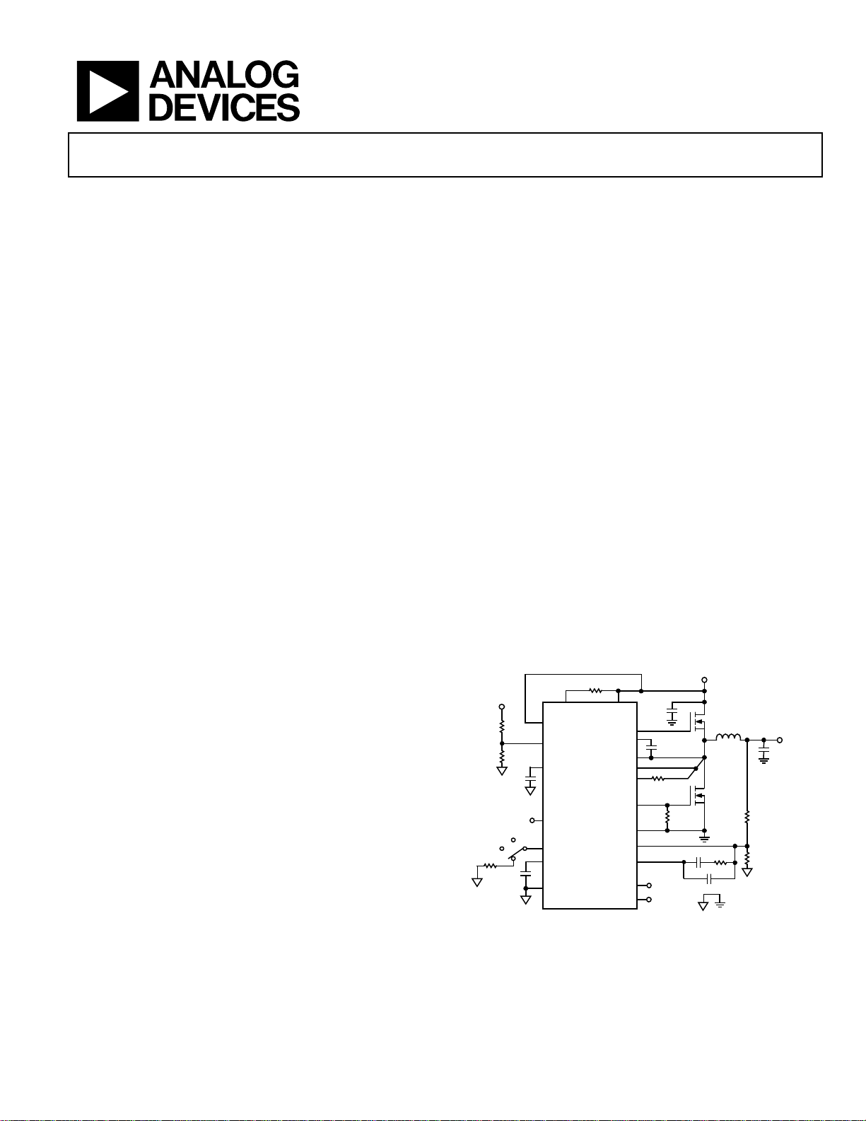
Figure 1. Typical Operation Circuit
www.analog.com

ADP1853 Data Sheet
TABLE OF CONTENTS
Features .............................................................................................. 1
Applications ....................................................................................... 1
General Description ......................................................................... 1
Revision History ............................................................................... 2
Specifications ..................................................................................... 3
Absolute Maximum Ratings ............................................................ 6
ESD Caution .................................................................................. 6
Simplified Block Diagram ............................................................... 7
Pin Configuration and Function Descriptions ............................. 8
Typical Performance Characteristics ........................................... 10
Theory of Operation ...................................................................... 12
Control Architecture .................................................................. 12
Oscillator Frequency .................................................................. 12
Synchronization .......................................................................... 13
PWM or Pulse Skip Mode of Operation ................................. 13
CLKOUT Signal .......................................................................... 13
Synchronous Rectifier and Dead Time ................................... 14
Input Undervoltage Lockout ..................................................... 14
Internal Linear Regulator .......................................................... 14
Overvolage Protection ............................................................... 14
Power Good ................................................................................. 14
Short-Circuit and Current-Limit Protection .......................... 15
Enable/Disable Control ............................................................. 15
Thermal Overload Protection .................................................. 16
Interleaved Dual-Phase Operation .......................................... 16
Applications Information .............................................................. 17
ADIsimPower Design Tool ....................................................... 17
Setting the Output Voltage ........................................................ 17
Soft Start ...................................................................................... 17
Setting the Current Limit .......................................................... 17
Accurate Current-Limit Sensing .............................................. 17
Input Capacitor Selection .......................................................... 17
VIN Pin Filter ............................................................................. 18
Boost Capacitor Selection ......................................................... 18
Inductor Selection ...................................................................... 18
Output Capacitor Selection....................................................... 18
MOSFET Selection ..................................................................... 19
Loop Compensation—Voltage Mode ...................................... 20
Loop Compensation—Current Mode ..................................... 21
Switching Noise and Overshoot Reduction ............................ 23
Voltage Tracking ......................................................................... 23
PCB Layout Guidlines ............................................................... 24
Typical Operating Circuits ............................................................ 25
Outline Dimensions ....................................................................... 27
Ordering Guide .......................................................................... 27
REVISION HISTORY
5/12—Revision 0: Initial Version
Rev. 0 | Page 2 of 28

Data Sheet ADP1853
POWER SUPPLY
TRSH
HYST
Quiescent Current
IIN
EN = VIN = 12 V, VFB = V
in forced pulse width
4.2
5.7
mA
CCO
IN_SD
TRK
TRK
CSG
CSG
CSG
CSG
Line Regulation of PWM
VFB/VIN
±0.015
%/V
COMP
COMP
OSCILLATOR
OSC
FREQ
FREQ
FREQ
SYNC
FREQ
SYNCMIN
SYNC
CLKOUT fOSC
CLKOUT
CLKOUT
VCCO
VCCO Load Regulation
I
VCCO
= 0 mA to 100 mA
35 mV
VCCO
DROPOUT
VCCO
SPECIFICATIONS
All limits at temperature extremes are guaranteed via correlation using standard statistical quality control (SQC). VIN = 12 V. The
specifications are valid for T
Table 1.
Parameter Symbol Test Conditions/Comments Min Typ Max Unit
Input Voltage VIN 2.75 20 V
Undervoltage Lockout Threshold UVLO
VIN falling 2.35 2.45 2.50 V
Undervoltage Lockout Hysteresis UVLO
EN = VIN = 12 V, VFB = V
Shutdown Current I
ERROR AMPLIFIER
FB Input Bias Current IFB −100 +1 +100 nA
Open-Loop Gain1 80 dB
Gain-Bandwidth Product1 20 MHz
TRK Input Bias Current I
CURRENT SENSE AMPLIFIER GAIN ACS Gain resistor connected to DL,
Gain resistor connected to DL,
Default setting, R
Voltage mode operation, resistor DL to PGND,
OUTPUT CHARACTERICTISTICS
Feedback Accuracy Voltage VFB
= −40°C to +125°C, unless otherwise specified. Typical values are at TA = 25°C.
J
VIN rising 2.55 2.65 2.75 V
0.2 V
modulation (PWM) mode (no switching)
CCO
in PSM mode 2.5 mA
EN = GND, VIN = 5.5 V or 20 V 100 200 µA
0 V ≤ V
≤ 5 V −100 +1 +100 nA
2.6 3 3.4 V/V
R
= 47 kΩ ± 5%
5.2 6 6.8 V/V
R
= 22 kΩ ± 5%
= open 10.5 12 13.5 V/V
0 V/V
R
= 100 kΩ ± 5%
TJ = −40°C to +85°C
TJ = −40°C to +125°C
597 600 603 mV
594 600 606 mV
Load Regulation of PWM1 VFB/V
Frequency f
R
R
R
V
range = 0.9 V to 2.2 V ±0.3 %
= 332 kΩ to AGND 170 200 230 kHz
= 78.7 kΩ to AGND 720 800 880 kHz
= 40.2 kΩ to AGND 1275 1500 1725 kHz
FREQ to AGND 240 300 360 kHz
FREQ to VCCO 480 600 720 kHz
SYNC Input Frequency Range1 f
SYNC Input Pulse Width1 t
SYNC Pin Capacitance to GND C
CLKOUT Frequency Range1 f
CLKOUT Pulse Duty Cycle D
CLKOUT Rise and Fall Time C
R
range from 332 kΩ to 40.2 kΩ 170 1725 kHz
100 ns
5 pF
range from 170 kHz to 1725 kHz 170 1725 kHz
50 %
= 47 pF 10 ns
LINEAR REGULATOR
VCCO Output Voltage I
VCCO Line Regulation VIN = 5.5 V to 20 V, I
= 100 mA 4.7 5.0 5.3 V
= 20 mA 10 mV
VCCO Current Limit1 VCCO drops to 4 V from 5 V 350 mA
VCCO Short-Circuit Current1 VCCO < 0.5 V 370 400 mA
VIN to VCCO Dropout Voltage2 V
I
= 100 mA, VIN ≤ 5 V 0.33 V
Rev. 0 | Page 3 of 28

ADP1853 Data Sheet
SYNC Logic Input Low
1.3
V
SYNC
BST
BST
DH or DL Driver RON, Sourcing
R
Sourcing 2 A with a 100 ns pulse
2
Ω
RON
OSC
OSC
OSC
OSC
OSC
COMP, THRES
COMP, HIGH
OVERVOLTAGE AND POWER GOOD
TRK
SOFT START
Parameter Symbol Test Conditions/Comments Min Typ Max Unit
LOGIC INPUTS
EN EN rising 0.57 0.63 0.68 V
EN Hysteresis 0.03 V
EN Input Leakage Current IEN VIN = 2.75 V to 20 V 1 200 nA
SYNC Logic Input High 1.9 V
SYNC Input Pull-Down Resistance R
GATE DRIVERS
DH Rise Time CDH = 3 n F, V
DH Fall Time CDH = 3 n F, V
DL Rise Time CDL = 3 nF 16 ns
DL Fall Time CDL = 3 nF 14 ns
DH to DL Dead Time External 3 nF is connected to DH and DL 25 ns
Current1
Sourcing 1 A with a 100 ns pulse, VIN = 3 V 2.3 Ω
DH or DL Driver RON, Tem p co TC
DH or DL Driver RON, Sinking
Current
1
Sinking 1 A with a 100 ns pulse, VIN = 3 V 2 Ω
DH Maximum Duty Cycle1 f
DH Maximum Duty Cycle1 f
Minimum DH On Time f
Minimum DH Off Time f
Minimum DL On Time f
COMP VOLTAGE RANGE
COMP Pulse Skip Threshold V
COMP Clamp High Voltage V
THERMAL SHUTDOWN
Thermal Shutdown Threshold T
Thermal Shutdown Hysteresis 20
1 MΩ
− VSW = 5 V 16 ns
− VSW = 5 V 14 ns
ON_SOURCE
VIN = 3 V or 12 V 0.3 %/oC
Sinking 2 A with a 100 ns pulse 1.5 Ω
R
ON_SINK
= 300 kHz 90 %
= 1500 kHz 50 %
= 200 kHz to 1500 kHz 85 ns
= 200 kHz to 1500 kHz 345 ns
= 200 kHz to 1500 kHz 295 ns
In pulse skip mode (PSM) 0.9 V
2.2 V
155
TMSD
°C
°C
THRESHOLDS
FB Overvoltage Threshold VOV VFB rising 0.630 0.65 0.670 V
FB Overvoltage Hysteresis 18 mV
FB Undervoltage Threshold VUV VFB falling 0.525 0.55 0.575 V
FB Undervoltage Hysteresis 15 mV
TRK INPUT VOLTAGE RANGE1 0 5 V
FB TO TRK OFFSET VOLTAGE TRK = 0.1 V to 0.57 V; offset = VFB − V
SS Output Current ISS During startup 4.6 6.5 8.4 µA
SS Pull-Down Resistor During a fault condition 3 kΩ
FB to SS offset VSS = 0.1 V to 0.6 V; offset = VFB − VSS −10 +10 mV
−10 0 +10 mV
Rev. 0 | Page 4 of 28
Data Sheet ADP1853
PGOOD
Parameter Symbol Test Conditions/Comments Min Typ Max Unit
PGOOD
PGOOD Pull-Up Resistor R
PGOOD Delay 12 µs
Overvoltage or Undervoltage
Minimum Duration
ILIM Threshold Voltage1 Relative to PGND −5 0 +5 mV
ILIM Output Current ILIM = PGND 45 50 55 µA
Current Sense Blanking Period After DL goes high, current limit is not sensed
INTEGRATED RECTIFIER
(BOOST DIODE) RESISTANCE
ZERO CURRENT CROSS OFFSET
(SW TO PGND)
1
Guaranteed by design.
2
Connect VIN to VCCO when VIN < 5.5 V.
1
Internal pull-up resistor to VCCO 12.5 kΩ
This is the minimum duration required to trip
10 µs
the PGOOD signal
100 ns
during this period
At 20 mA forward current 16 Ω
In pulse skip mode only; f
= 300 kHz 0 2 4 mV
OSC
Rev. 0 | Page 5 of 28
ADP1853 Data Sheet
BST to SW
−0.3 V to +6 V
BST to PGND to PGND 20 ns Transients
32 V
1, 2
ABSOLUTE MAXIMUM RATINGS
Table 2.
Parameter Rating
VIN, EN, RAMP 21 V
FB, COMP, SS, TRK, FREQ, SYNC, VCCO,
−0.3 V to +6 V
PGOOD, CLKOUT
ILIM, SW, CS to PGND −0.3 V to +21 V
BST, DH to PGND −0.3 V to +28 V
DL to PGND −0.3 V to VCCO + 0.3 V
SW, CS to PGND 20 ns Transients 25 V
DL, SW, CS, ILIM to PGND 20 ns
−8 V
Negative Transients
PGND to AGND −0.3 V to +0.3 V
PGND to AGND 20 ns Transients −8 V to +4 V
θJA (Natural Convection)
40°C/W
Operating Junction Temperature Range3 −40°C to +125°C
Storage Temperature Range −65°C to +150°C
Maximum Soldering Lead Temperature 260°C
1
Measured with exposed pad attached to PCB.
2
Junction-to-ambient thermal resistance (θJA) of the package was calculated
or simulated on multilayer PCB.
3
The junction temperature (TJ) of the device is dependent on the ambient
temperature (T
ambient thermal resistance of the package (θ
temperature is calculated from the ambient temperature and power
dissipation using the formula T
) the power dissipation of the device (PD) and the junction to
A
= TA + PD × θJA.
J
). Maximum junction
JA
Stresses above those listed under Absolute Maximum Ratings
may cause permanent damage to the device. This is a stress
rating only; functional operation of the device at these or any
other conditions above those indicated in the operational
section of this specification is not implied. Exposure to absolute
maximum rating conditions for extended periods may affect
device reliability.
Absolute maximum ratings apply individually only, not in
combination. Unless otherwise specified, all other voltages are
referenced to GND.
ESD CAUTION
Rev. 0 | Page 6 of 28
Data Sheet ADP1853
BST
PGND
+
–
+
–
+
–
+
–
FB
OV_TH
UV_TH
PGOOD
CURRENT SENSE
AMPLIFIER
DH
DL
ILIM
SW
V
REF
= 0.6V
+
+
–
ERROR
AMPLIFIER
FB
COMP
SS
PWM
COMPARATOR
SLOPE COMPENSATION
AND RAMP GENERAT OR
CURRENT-LIMIT
CONTROL
RAMP
50µA
OV
+
TRK
CS GAIN
DRIVER LOGIC
CONTROL AND
STATE
MACHINE
OVER_LIM
PULSE SKIP
OVER_LIM
LDO
LOGIC
EN
VIN
UVLO
OSCILLATOR
FREQ
SYNC
REF
VCCO
OV
UV
0.6V
THERMAL
SHUTDOWN
AGND
CS
FAULT
OV
LOGIC
OVER_LIM
OV
EN
EN_SW
LOGIC
UV
3kΩ
0.9V
DCM
*0 (ZERO) GAIN IS FOR VOLTAGE MODE WITH RAMP FROM 0.7V TO 2.2V.
ZERO
CROSS
DETECT
12.5kΩ
A
V
= 0,* 3, 6, 12
VCCO
CLK
EN_SW
1MΩ
–
+
CLKOUT
VCCO
VCCO
VCCO
VCCO
SLAVE
SL_TH
FB
SLAVE
0.6V
6.5µA
10594-002
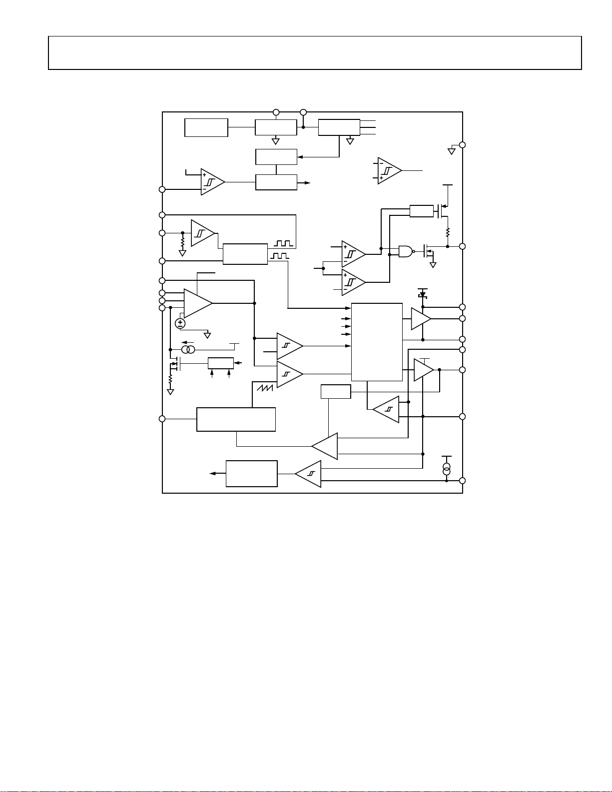
SIMPLIFIED BLOCK DIAGRAM
Rev. 0 | Page 7 of 28
Figure 2.
ADP1853 Data Sheet
15
BST
Boot Strapped Upper Rail of High-Side Internal Driver. Connect a 0.1 µF to a 0.22 µF multilayer ceramic capacitor
14
13
12
1
3
4
DH
15
BST
NOTES
1. CONNECT THE BOTTOM OF THE
EXPOSED PAD TO THE SYSTEM
AGND PLANE.
SW
CS
11
DL
EN
FB
2
SS
COMP
5
AGND
7
CLKOUT
6
SYNC
8
VIN
9
VCCO
10
PGND
19
FREQ
20
TRK
18
RAMP
17
PGOOD
16
ILIM
ADP1853
TOP VIEW
10594-003
PIN CONFIGURATION AND FUNCTION DESCRIPTIONS
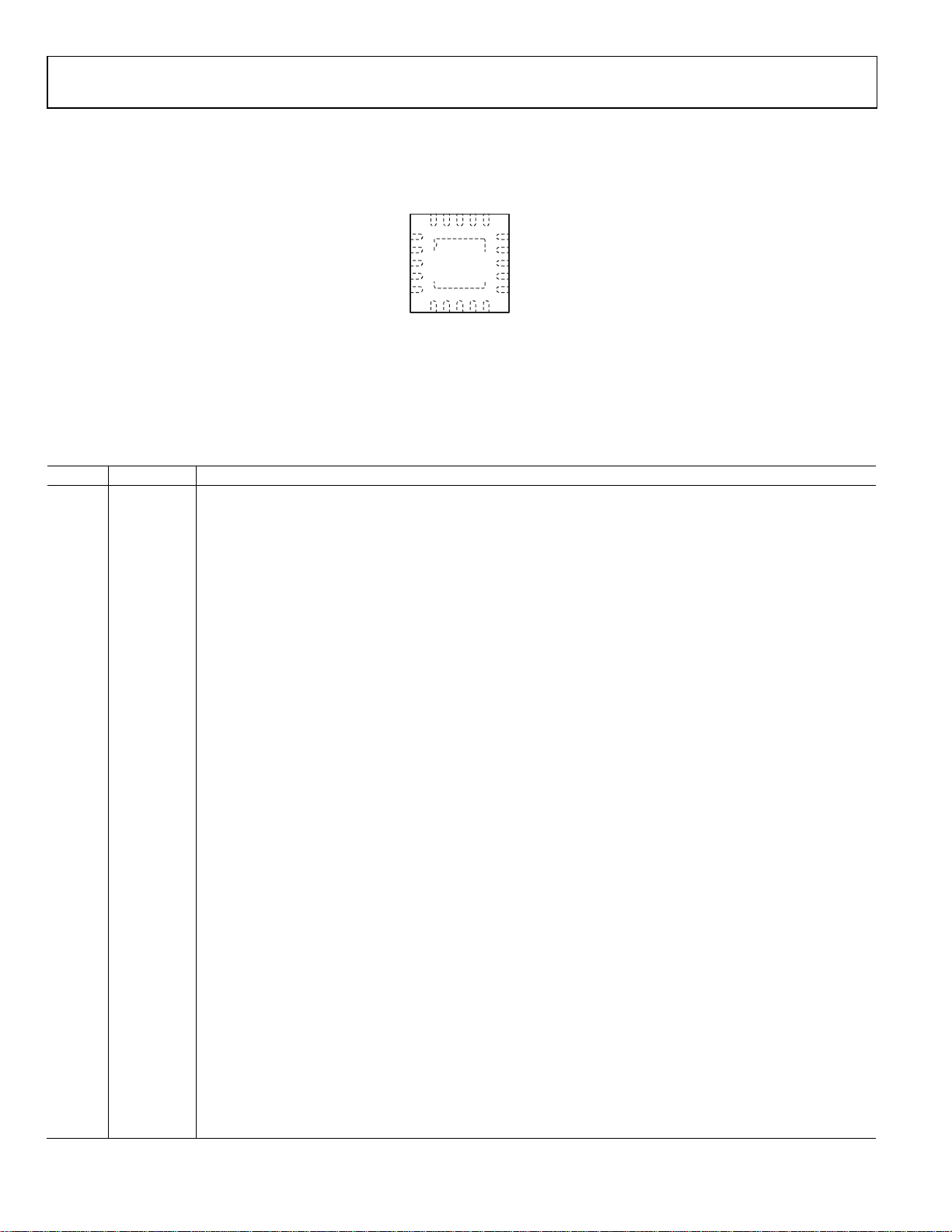
Figure 3. Pin Configuration
Table 3. Pin Function Descriptions
Pin No. Mnemonic Description
1 EN Enable Input. Drive EN high to turn on the controller, and drive EN low to turn the controller off. Tie EN to VIN for
automatic startup. For a precision UVLO, put an appropriately sized resistor divider from V
midpoint to this pin.
2 SS Soft Start Input. Connect a capacitor from SS to AGND to set the soft start period. This node is internally pulled up
to VCCO through a 6.5 µA current source.
3 FB Output Voltage Feedback. Connect this pin to an output via a resistor divider. Tie FB to VCCO for slave mode
operation in interleaved dual-phase configuration.
4 COMP Compensation Node. Output of the error amplifier. Connect a resistor-capacitor network from COMP to FB to
compensate the regulation control loop. In interleaved dual-phase configuration, tie this pin to the COMP pin of
the second channel.
5 AGND Analog Ground. Connect to the system AGND plane.
6 SYNC Frequency Synchronization Input. This pin accepts an external clock signal with a frequency close to 1× the
internal oscillator frequency, f
, set by the FREQ pin. The controller operates in forced PWM when a periodic clock
OSC
signal is detected at SYNC or when SYNC is high. The resulting switching frequency is 1× the SYNC frequency.
When SYNC is low or left floating, the controller operates in pulse skip mode.
7 CLKOUT
Internal Clock Output. The CLKOUT is 1× the internal oscillator or input SYNC signal frequency, 180° phase-shifted.
This pin can be used to synchronize another
ADP1853 or other controllers.
8 VIN Connect to Main Power Supply. Bypass with a 1 µF or larger ceramic capacitor connected as close to this pin as
possible and AGND.
9 VCCO Output of the Internal Low Dropout Regulator (LDO). The internal circuitry and gate drivers are powered from
VCCO. Bypass VCCO to AGND with a 1 μF or larger ceramic capacitor. The VCCO output remains active even when
EN is low. For operations at V
below 5 V, VIN may be jumped to VCCO. Do not use the LDO to power other auxiliary
IN
system loads.
10 PGND Power Ground. Ground for internal driver. Differential current.
11 DL Low-Side Synchronous Rectifier Gate Driver Output. To program the gain of the current sense amplifier in a current
mode or to set voltage mode control, connect a resistor between DL and PGND. This pin is capable of driving
MOSFETs with a total input capacitance up to 20 nF.
12 CS Current Sense Amplifier Input. Differential current is sensed between CS and PGND. Connect this pin to the
current sense resistor or to the SW pin to sense the current. Tie this pin to PGND for voltage mode operation.
13 SW Power Switch Node. Connect this pin to the source of the high-side N-channel MOSFET and the drain of the low-
14 DH High-Side Switch Gate Driver Output. This pin is capable of driving MOSFETs with a total input capacitance up to
16 ILIM Current-Limit Sense Comparator Inverting Input. Connect a resistor between ILIM and SW to set the current-
side N-channel MOSFET.
20 nF.
(MLCC) between BST and SW. There is an internal boost diode rectifier connected between VCCO and BST.
limit offset. For accurate current-limit sensing, connect ILIM to a current sense resistor at the source of the
low-side MOSFET.
Rev. 0 | Page 8 of 28
to AGND, and tie the
IN

Data Sheet ADP1853
Pin No. Mnemonic Description
17 PGOOD Power Good. The open-drain power good indicator logic output with an internal 12.5 kΩ resistor is connected
between PGOOD and VCCO. PGOOD is pulled to ground when the output is outside the regulation window. An
external pull-up resistor is not required. If the controller is configured as a slave in the interleaved dual-phase
application by tying the FB pin high to VCCO, the pulse skip mode is enabled by driving the PGOOD pin low
externally in cases when the master is in pulse skip mode at light loads. Otherwise, if the master is configured to
forced PWM operation, PGOOD of the slave controller must be connected to the PGOOD of the master.
18 RAMP Programmable Current Setting for Slope Compensation. Connect a resistor from RAMP to VIN. The voltage at RAMP
is 0.2 V during operation. This pin is high impedance when the channel is disabled.
19 FREQ Internal Oscillator Frequency, f
resistor between FREQ and AGND. Connect FREQ to AGND for a preprogrammed 300 kHz or tie FREQ to VCCO for
600 kHz operating frequency.
20 TRK Tracking Input. Connect TRK to VCCO if tracking is not used.
EPAD Exposed Pad. Connect the bottom of the exposed pad to the system AGND plane.
. Sets the desired operating frequency between 200 kHz and 1.5 MHz with one
OSC
Rev. 0 | Page 9 of 28
 Loading...