ANALOG DEVICES ADP1829 Service Manual
Dual, Interleaved, Step-Down
V
V
www.BDTIC.com/ADI
FEATURES
Fixed frequency operation: 300 kHz, 600 kHz, or
synchronized operation up to 1 MHz
Supply input range: 3.0 V to 18 V
Wide power stage input range: 1 V to 24 V
Interleaved operation results in smaller, low cost
input capacitor
All-N-channel MOSFET design for low cost
±0.85% accuracy at 0°C to 70°C
Soft start, thermal overload, current-limit protection
10 μA shutdown supply current
Internal linear regulator
Lossless R
Reverse current protection during soft start for handling
precharged outputs
Independent Power OK outputs
Voltage tracking for sequencing or DDR termination
Available in 5 mm × 5 mm, 32-lead LFCSP
APPLICATIONS
Telecommunications and networking systems
Medical imaging systems
Base station power
Set-top boxes
Printers
DDR termination
current-limit sensing
DSON
DC-to-DC Controller with Tracking
ADP1829
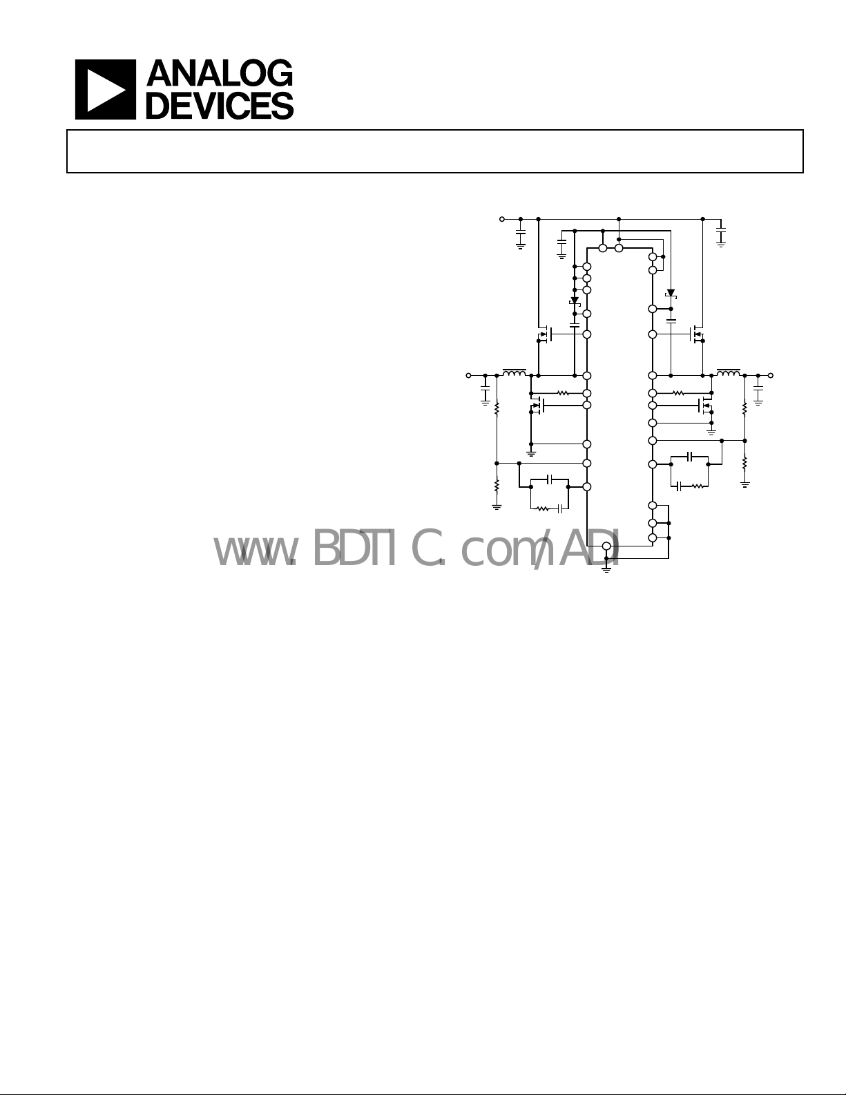
TYPICAL APPLICATION CIRCUIT
= 12
IN
390pF
4.53kΩ
180µF
IRLR7807Z
2kΩ
1kΩ
1.8V,
8A
560µF560µF
1.2V,
6A
180µF
IRLR7807Z
1µF
EN1
PV IN
TRK1
EN2
TRK2
VREG
BST2
0.47µF
2.2µH 2.2µH
2kΩ
IRFR3709Z
2kΩ
4.53kΩ
BST1
DH2
DH1
ADP1829
SW2
SW1
2kΩ 2kΩ
390pF
3900pF
CSL1
DL1
PGND1
FB1
COMP1
GND
Figure 1.
CSL2
DL2
PGND2
FB2
COMP2
FREQ
LDOSD
SYNC
0.47µF
IRFR3709Z
3900pF
06784-001
GENERAL DESCRIPTION
The ADP1829 is a versatile, dual, interleaved, synchronous
PWM buck controller that generates two independent output
rails from an input of 3.0 V to 18 V, with power input voltage
ranging from 1.0 V to 24 V. Each controller can be configured
to provide output voltages from 0.6 V to 85% of the input
voltage and is sized to handle large MOSFETs for point-of-load
regulators. The two channels operate 180° out of phase,
reducing stress on the input capacitor and allowing smaller, low
cost components. The ADP1829 is ideal for a wide range of
high power applications, such as DSP and processor core I/O
power, and general-purpose power in telecommunications,
medical imaging, PC, gaming, and industrial applications.
The ADP1829 operates at a pin-selectable, fixed switching
frequency of either 300 kHz or 600 kHz, minimizing external
component size and cost. For noise-sensitive applications, it can
also be synchronized to an external clock to achieve switching
Rev. 0
Information furnished by Analog Devices is believed to be accurate and reliable. However, no
responsibility is assumed by Anal og Devices for its use, nor for any infringements of patents or ot her
rights of third parties that may result from its use. Specifications subject to change without notice. No
license is granted by implication or otherwise under any patent or patent rights of Analog Devices.
Trademarks and registered trademarks are the property of their respective owners.
frequencies between 300 kHz and 1 MHz. The ADP1829
includes soft start protection to prevent inrush current from the
input supply during startup, reverse current protection during
soft start for precharged outputs, as well as a unique adjustable
lossless current-limit scheme utilizing external MOSFET sensing.
For applications requiring power supply sequencing, the
ADP1829 also provides tracking inputs that allow the output
voltages to track during startup, shutdown, and faults. This
feature can also be used to implement DDR memory bus
termination.
The ADP1829 is specified over the −40°C to +125°C junction
temperature range and is available in a 32-lead LFCSP package.
One Technology Way, P.O. Box 9106, Norwood, MA 02062-9106, U.S.A.
Tel: 781.329.4700 www.analog.com
Fax: 781.461.3113 ©2007 Analog Devices, Inc. All rights reserved.

ADP1829
www.BDTIC.com/ADI
TABLE OF CONTENTS
Features.............................................................................................. 1
Applications....................................................................................... 1
Typical Application Circuit ............................................................. 1
General Description ......................................................................... 1
Revision History ............................................................................... 2
Specifications..................................................................................... 3
Absolute Maximum Ratings............................................................ 5
ESD Caution.................................................................................. 5
Functional Block Diagram .............................................................. 6
Pin Configuration and Function Descriptions............................. 7
Typical Performance Characteristics ............................................. 9
Theory of Operation ...................................................................... 13
Input Power .................................................................................13
Start-Up Logic............................................................................. 13
Internal Linear Regulator.......................................................... 13
Oscillator and Synchronization ................................................ 13
Error Amplifier........................................................................... 14
Soft Start ...................................................................................... 14
Power OK Indicator ...................................................................14
Tracking ....................................................................................... 14
MOSFET Drivers........................................................................ 15
Current Limit.............................................................................. 15
Applications Information.............................................................. 16
Selecting the Input Capacitor................................................... 16
Selecting the MOSFETs ............................................................. 17
Setting the Current Limit.......................................................... 18
Feedback Voltage Divider ......................................................... 18
Compensating the Voltage Mode Buck Regulator................. 19
Soft Start ...................................................................................... 22
Voltage Tracking......................................................................... 22
Coincident Tracking .................................................................. 23
Ratiometric Tracking................................................................. 23
Thermal Considerations............................................................ 24
PCB Layout Guidelines.................................................................. 25
LFCSP Package Considerations................................................ 26
Application Circuits ....................................................................... 27
Outline Dimensions....................................................................... 29
Ordering Guide .......................................................................... 29
REVISION HISTORY
6/07—Revision 0: Initial Version
Rev. 0 | Page 2 of 32
ADP1829
www.BDTIC.com/ADI
SPECIFICATIONS
IN = 12 V, ENx = FREQ = PV = VREG = 5 V, SYNC = GND, TJ = −40°C to +125°C, unless otherwise specified. All limits at temperature
extremes are guaranteed via correlation using standard statistical quality control (SQC). Typical values are at T
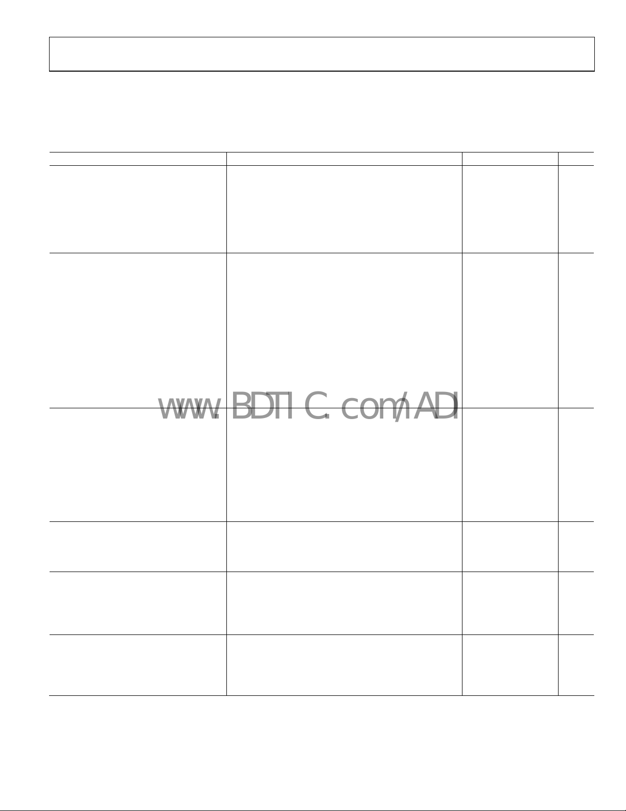
Table 1.
Parameter Conditions Min Typ Max Unit
POWER SUPPLY
IN Input Voltage PV = VREG (using internal regulator) 5.5 18 V
IN = PV = VREG (not using internal regulator) 3.0 5.5 V
IN Quiescent Current Not switching, I
= 0 mA 1.5 3 mA
VREG
IN Shutdown Current EN1 = EN2 = GND 10 20 μA
VREG Undervoltage Lockout Threshold VREG rising 2.4 2.7 3.0 V
VREG Undervoltage Lockout Hysteresis 0.125 V
ERROR AMPLIFIER
FB1, FB2 Regulation Voltage
= 25°C, TRK1, TRK2 > 700 mV
T
A
= 0°C to 85°C, TRK1, TRK2 > 700 mV
T
J
= −40°C to +125°C, TRK1, TRK2 > 700 mV
T
J
= 0°C to 70°C, TRK1, TRK2 > 700 mV
T
J
FB1, FB2 Input Bias Current 100 nA
Open-Loop Voltage Gain 70 dB
Gain-Bandwidth Product 20 MHz
COMP1, COMP2 Sink Current 600 μA
COMP1, COMP2 Source Current 120 μA
COMP1, COMP2 Clamp High Voltage 2.4 V
COMP1, COMP2 Clamp Low Voltage 0.75 V
LINEAR REGULATOR
VREG Output Voltage
IN = 7 V to 18 V, I
VREG Load Regulation I
VREG Line Regulation IN = 7 V to 18 V, I
= 25°C, I
T
A
= 0 mA to 100 mA, IN = 12 V −40 mV
VREG
= 20 mA
VREG
= 0 mA to 100 mA 4.75 5.0 5.25 V
VREG
= 20 mA 1 mV
VREG
VREG Current Limit VREG = 4 V 220 mA
VREG Short-Circuit Current VREG < 0.5 V 95 140 200 mA
IN to VREG Dropout Voltage
1
I
= 100 mA, IN < 5 V 0.7 1.4 V
VREG
VREG Minimum Output Capacitance 1 μF
PWM CONTROLLER
PWM Ramp Voltage Peak SYNC = GND 1.3 V
DH1, DH2 Maximum Duty Cycle FREQ = GND (300 kHz) 91 93 %
DH1, DH2 Minimum Duty Cycle FREQ = GND (300 kHz) 1 3 %
SOFT START
SS1, SS2 Pull-Up Resistance SS1, SS2 = GND 90 kΩ
SS1, SS2 Pull-Down Resistance SS1, SS2 = 0.6 V 6 kΩ
SS1, SS2 to FB1, FB2 Offset Voltage SS1, SS2 = 0 mV to 500 mV −45 mV
SS1, SS2 Pull-Up Voltage 0.8 V
TRACKING
TRK1, TRK2 Common-Mode Input
0 600 mV
Voltage Range
TRK1, TRK2 to FB1, FB2 Offset Voltage TRK1, TRK2 = 0 mV to 500 mV −5 +5 mV
TRK1, TRK2 Input Bias Current 100 nA
= 25°C.
A
597 600 603 mV
591 609 mV
588 612 mV
595 605 mV
4.85 5.0 5.15 V
Rev. 0 | Page 3 of 32

ADP1829
www.BDTIC.com/ADI
Parameter Conditions Min Typ Max Unit
OSCILLATOR
Oscillator Frequency SYNC = FREQ = GND (fSW = f
SYNC = GND, FREQ = VREG (fSW = f
SYNC Synchronization Range
2
FREQ = GND, SYNC = 600 kHz to 1.2 MHz (fSW = f
FREQ = VREG, SYNC = 1.2 MHz to 2 MHz (fSW = f
SYNC Minimum Input Pulse Width 200 ns
CURRENT SENSE
CSL1, CSL2 Threshold Voltage Relative to PGND −30 0 +30 mV
CSL1, CSL2 Output Current CSL1, CSL2 = PGND 44 50 56 μA
Current Sense Blanking Period 100 ns
GATE DRIVERS
DH1, DH2 Rise Time CDH = 3 nF, V
DH1, DH2 Fall Time CDH = 3 nF, V
− VSW = 5 V 15 ns
BST
− VSW = 5 V 10 ns
BST
DL1, DL2 Rise Time CDL = 3 nF 15 ns
DL1, DL2 Fall Time CDL = 3 nF 10 ns
DH to DL, DL to DH Dead Time 40 ns
LOGIC THRESHOLDS
SYNC, FREQ, LDOSD Input High Voltage 2.2 V
SYNC, FREQ, LDOSD Input Low Voltage 0.4 V
SYNC, FREQ Input Leakage Current SYNC, FREQ = 0 V to 5.5 V 1 μA
LDOSD Pull-Down Resistance 100 kΩ
EN1, EN2 Input High Voltage IN = 3.0 V to 18 V 2.0 V
EN1, EN2 Input Low Voltage IN = 3.0 V to 18 V 0.8 V
EN1, EN2 Current Source EN1, EN2 = 0 V to 3.0 V −0.3 −0.6 −1.5 μA
EN1, EN2 Input Impedance to 5 V Zener EN1, EN2 = 5.5 V to 18 V 100 kΩ
THERMAL SHUTDOWN
Thermal Shutdown Threshold
Thermal Shutdown Hysteresis
3
3
145
15
POWER GOOD
FB1, UV2 Overvoltage Threshold V
rising 750 mV
FB1, VUV2
FB1, UV2 Overvoltage Hysteresis 50 mV
FB1, UV2 Undervoltage Threshold V
rising 550 mV
FB1, VUV2
FB1, UV2 Undervoltage Hysteresis 50 mV
POK1, POK2 Propagation Delay 8 μs
POK1, POK2 Off Leakage Current V
POK1, POK2 Output Low Voltage I
POK1, VPOK2
POK1, IPOK2
= 5.5 V 1 μA
= 10 mA 150 500 mV
UV2 Input Bias Current 10 100 nA
1
Not recommended to use the LDO in dropout when VIN < 5.5 V because of the dropout voltage. Connect IN to VREG when VIN < 5.5 V.
2
SYNC input frequency is 2× single-channel switching frequency. The SYNC frequency is divided by 2 and the separate phases were used to clock the controllers.
3
Guaranteed by design and not subject to production test.
) 240 300 370 kHz
OSC
) 480 600 720 kHz
OSC
/2) 300 600 kHz
SYNC
/2) 600 1000 kHz
SYNC
°C
°C
Rev. 0 | Page 4 of 32
ADP1829
www.BDTIC.com/ADI
ABSOLUTE MAXIMUM RATINGS
Table 2.
Parameter Rating
IN, EN1, EN2 −0.3 V to +20 V
BST1, BST2 −0.3 V to +30 V
BST1, BST2 to SW1, SW2 −0.3 V to +6 V
CSL1, CSL2 −1 V to +30 V
SW1, SW2 −2 V to +30 V
DH1 SW1 − 0.3 V to BST1 + 0.3 V
DH2 SW2 − 0.3 V to BST2 + 0.3 V
DL1, DL2 to PGND −0.3 V to PV + 0.3 V
PGND to GND ±2 V
LDOSD, SYNC, FREQ, COMP1,
−0.3 V to +6 V
COMP2, SS1, SS2, FB1, FB2, VREG,
PV, POK1, POK2, TRK1, TRK2
θJA 4-Layer
(JEDEC Standard Board)
1, 2
45°C/W
Operating Ambient Temperature −40°C < TA< +85°C
Operating Junction Temperature3−40°C < TJ < +125°C
Storage Temperature −65°C to +150°C
1
Measured with exposed pad attached to PCB.
2
Junction-to-ambient thermal resistance (θJA) of the package is based on
modeling and calculation using a 4-layer board. The junction-to-ambient
thermal resistance is application and board-layout dependent. In applications where high maximum power dissipation exists, attention to thermal
dissipation issues in board design is required. For more information, refer to
Application Note AN-772, A Design and Manufacturing Guide for the Lead
Frame Chip Scale Package (LFCSP).
3
In applications where high power dissipation and poor package thermal
resistance are present, the maximum ambient temperature may have to be
derated. Maximum ambient temperature (T
maximum operating junction temperature (T
power dissipation of the device in the application (P
to-ambient thermal resistance of the part/package in the application (θJA)
and is given by the following equation: T
) is dependent on the
A_MAX
= 125oC), the maximum
J_MAX_OP
D_MAX
= T
A_MAX
J_MAX_OP
), and the junction-
– (θJA × P
D_MAX
).
Stresses above those listed under Absolute Maximum Ratings
may cause permanent damage to the device. This is a stress
rating only; functional operation of the device at these or any
other conditions above those indicated in the operational
section of this specification is not implied. Exposure to absolute
maximum rating conditions for extended periods may affect
device reliability.
ESD CAUTION
Rev. 0 | Page 5 of 32
ADP1829
www.BDTIC.com/ADI
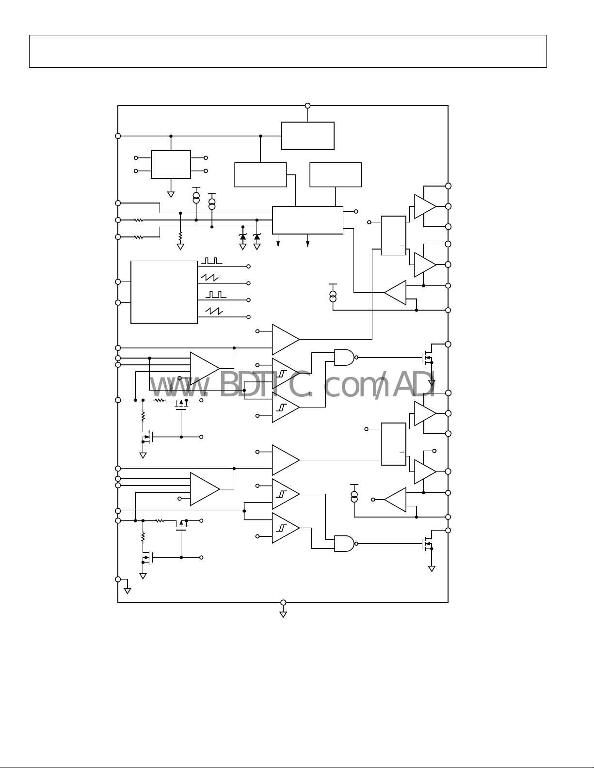
FUNCTIONAL BLOCK DIAGRAM
VREG
0.75V
0.55V
VREG
–
+
+
+
0.8V
FAULT1
–
+
+
+
0.8V
FAULT2
VREG
LDOSD
EN1
EN2
FREQ
SYNC
COMP1
FB1
TRK1
SS1
COMP2
FB2
TRK2
UV2
SS2
0.6V
0.8V
OSCILLATOR
PHASE 1 = 0°
PHASE 2 = 180°
REF
0.6V
0.6V
CK1
RAMP1
CK2
RAMP2
RAMP1
RAMP2
0.75V
0.55V
0.75V
0.55V
UVLO
+
–
+
–
+
–
+
–
+
–
+
–
IN
LINEAR REG
LOGIC
FAULT2FAULT1
50µA
THERMAL
SHUTDOWN
VREG
50µA
ILIM2
CK2
VREG
ILIM1
CK1
ILIM2
PWM
R
PWM
R
ADP1829
QS
Q
+
–
QS
Q
+
–
BST1
DH1
SW1
PV
DL1
PGND1
CSL1
POK1
BST2
DH2
SW2
PV
DL2
PGND2
CSL2
POK2
GND
BOTTOM PADDLE
OF LFCSP
Figure 2.
Rev. 0 | Page 6 of 32
06784-002
ADP1829
www.BDTIC.com/ADI
PIN CONFIGURATION AND FUNCTION DESCRIPTIONS
OMP1
S1
C
TRK1
S
LDOSD
VREG
EN2
IN
EN1
27
29
26
28
31
30
32
25
1FB1
2SYNC
3FREQ
4GND
5UV2
6FB2
7COMP2
8TRK2
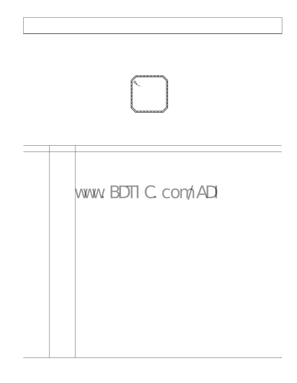
PIN 1
INDICAT OR
ADP1829
TOP VIEW
(Not to Scale)
9
11
12
10
SS2
DH2
BST2
POK2
13
2
SW
24 POK1
23 BST1
22 DH1
21 SW1
20 CSL1
19 PGND1
18 DL1
17 PV
14
15
16
DL2
CSL2
PGND2
06784-003
Figure 3. ADP1829 Pin Configuration
Table 3. Pin Function Descriptions
Pin No. Mnemonic Description
1 FB1
2 SYNC
Feedback Voltage Input for Channel 1. Connect a resistor divider from the buck regulator output to GND and tie
the tap t
o FB1 to set the output voltage.
Frequency Synchronization Input. Accepts external signal between 600 kHz and 1.2 MHz or between 1.2 MHz
and 2 MH
z depending on whether FREQ is low or high, respectively. Connect SYNC to ground if not used.
3 FREQ Frequency Select Input. Low for 300 kHz or high for 600 kHz.
4 GND
5 UV2
Ground. Connect to a ground plane directly beneath the ADP1829. Tie the bottom of the feedback dividers to
this GND
Input to the POK2 Undervoltage and Overvoltage Compar
.
ators. For the default thresholds, connect UV2
directly to FB2. For some tracking applications, connect UV2 to an extra tap on the FB2 voltage divider string.
6 FB2
Voltage Feedback Input for Channel 2. Connect a resistor divider fr
om the buck regulator output to GND and
tie the tap to FB2 to set the output voltage.
7 COMP2 Error Amplifier Output for Channel 2. Connect an RC network from COMP2 to FB2 to compensate Channel 2.
8 TRK2
Tracking Input for Channel 2. To track a master voltage
, drive TRK2 from a voltage divider from the master
voltage. If the tracking function is not used, connect TRK2 to VREG.
9 SS2 Soft Start Control Input. Connect a capacitor from SS2 to GND to set the soft start period.
10 POK2
Open-Drain Power OK Output for Channel 2. Sinks current when UV2 is out of r
egulation. Connect a pull-up
resistor from POK2 to VREG.
11 BST2
Boost Capacitor Input for Channel 2. Powers the high-side ga
te driver DH2. Connect a 0.22 μF to 0.47 μF
ceramic capacitor from BST2 to SW2 and a Schottky diode from PV to BST2.
12 DH2 High-Side (Switch) Gate Driver Output for Channel 2.
13 SW2 Switch Node Connection for Channel 2.
14 CSL2
Current Sense Comparator Inverting Input for Channel 2. C
onnect a resistor between CSL2 and SW2 to set the
current-limit offset.
15 PGND2 Ground for Channel 2 Gate Driver. Connect to a ground plane directly beneath the ADP1829.
16 DL2 Low-Side (Synchronous Rectifier) Gate Driver Output for Channel 2.
17 PV
Positive Input Voltage for Gate Driver DL1 and Gate Driver DL2. C
onnect PV to VREG and bypass to ground with
a 1 μF capacitor.
18 DL1 Low-Side (Synchronous Rectifier) Gate Driver Output for Channel 1.
19 PGND1 Ground for Channel 1 Gate Driver. Connect to a ground plane directly beneath the ADP1829.
20 CSL1
Current Sense Comparator Inverting Input for Channel 1. C
onnect a resistor between CSL1 and SW1 to set the
current-limit offset.
21 SW1 Switch Node Connection for Channel 1.
22 DH1 High-Side (Switch) Gate Driver Output for Channel 1.
23 BST1
Boost Capacitor Input for Channel 1. Powers the high-side ga
te driver DH1. Connect a 0.22 μF to 0.47 μF
ceramic capacitor from BST1 to SW1 and a Schottky diode from PV to BST1.
24 POK1
Open-Drain Power OK Output for Channel 1. Sinks current when FB1 is out of r
egulation. Connect a pull-up
resistor from POK1 to VREG.
Rev. 0 | Page 7 of 32
ADP1829
www.BDTIC.com/ADI
Pin No. Mnemonic Description
25 EN1
26 EN2
27 LDOSD
28 IN
29 VREG
30 SS1 Soft Start Control Input. Connect a capacitor from SS1 to GND to set the soft start period.
31 TRK1
32 COMP1 Error Amplifier Output for Channel 1. Connect an RC network from COMP1 to FB1 to compensate Channel 1.
Enable Input for Channel 1. Drive EN1 high to turn on the Chann
Enabling starts the internal LDO. Tie to IN for automatic startup.
Enable Input for Channel 2. Drive EN2 high to turn on the Chann
Enabling starts the internal LDO. Tie to IN for automatic startup.
LDO Shut-Down Input. Only used to shut do
Otherwise, connect LDOSD to GND or leave it open, as it has an internal 100 kΩ pull-down resistor.
Input Supply to the Internal Linear Regulator. Drive IN with 5.5
For input voltages between 3.0 V and 5.5 V, tie IN to VREG and PV.
Output of the Internal Linear Regulator (LDO). The internal cir
Bypass VREG to ground plane with 1 μF ceramic capacitor.
Tracking Input for Channel 1. To track a master voltage, dr
If the tracking function is not used, connect TRK1 to VREG.
wn the LDO in those applications where IN is tied directly to VREG.
el 1 controller, and drive it low to turn off.
el 2 controller, and drive it low to turn off.
V to 18 V to power the ADP1829 from the LDO.
cuitry and gate drivers are powered from VREG.
ive TRK1 from a voltage divider to the master voltage.
Rev. 0 | Page 8 of 32
ADP1829
www.BDTIC.com/ADI
TYPICAL PERFORMANCE CHARACTERISTICS
95
90
85
80
EFFICIE NCY (%)
75
VIN = 5V
VIN = 12V
VIN = 20V
VIN = 15V
92
90
88
86
84
EFFICIE NCY (%)
82
80
SWITCHING FREQUENCY = 300kHz
SWITCHI NG FREQUENCY = 600kHz
70
020
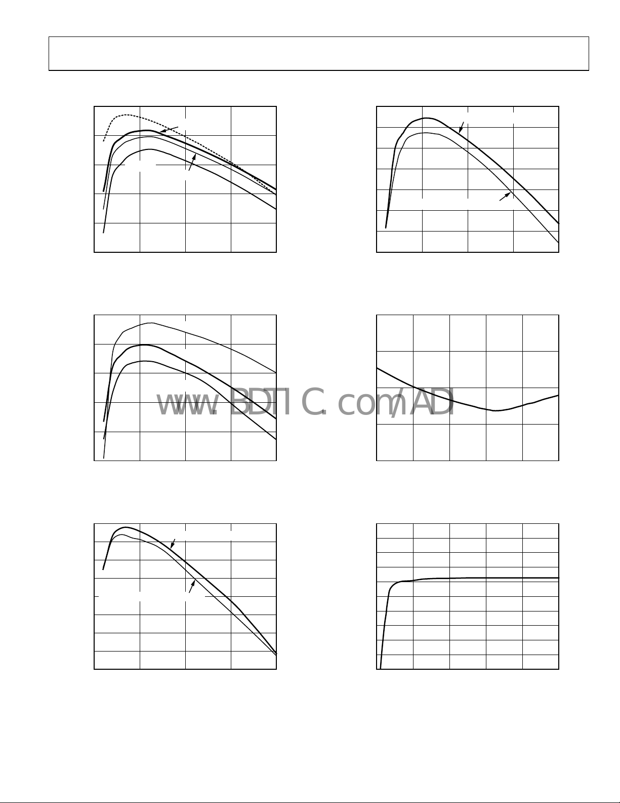
Figure 4. Efficiency vs. Load Current, V
95
90
85
80
EFFICIE NCY (%)
75
70
020
Figure 5. Efficiency vs. Load Current, V
94
92
90
88
86
SWITCHING FREQUENCY = 600kHz
84
EFFICIE NCY (%)
82
80
78
020
Figure 6. Efficiency vs. Load Current, V
51015
LOAD CURRENT (A)
= 1.8 V, 300 kHz Switching
OUT
V
= 3.3V
OUT
V
= 1.8V
OUT
V
= 1.2V
OUT
51015
LOAD CURRENT (A)
= 12 V, 300 kHz Switching
IN
SWITCHING FREQUENCY = 300kHz
51015
LOAD CURRENT (A)
= 5 V, V
IN
OUT
= 1.8 V
06784-004
06784-005
06784-006
78
020
Figure 7. Efficiency vs. Load Current, V
4.980
4.975
4.970
VREG VOLTAGE (V)
4.965
4.960
–40 85
Figure 8. VREG Voltage vs. Temperature
4.970
4.968
4.966
4.964
4.962
4.960
VREG (V)
4.958
4.956
4.954
4.952
4.950
520
Figure 9. VREG vs. Input Voltage, 10 mA Load
51015
LOAD CURRENT (A)
= 12 V, V
IN
–15103560
TEMPERATURE ( °C)
8 111417
INPUT VOLTAGE (V)
OUT
= 1.8 V
06784-007
06784-008
06784-009
Rev. 0 | Page 9 of 32
ADP1829
www.BDTIC.com/ADI
4.960
0.6010
4.956
4.952
VREG (V)
4.948
4.944
4.940
0 100
5
4
3
2
VREG OUTPUT (V)
1
20 40 60 80
LOAD CURRENT (mA)
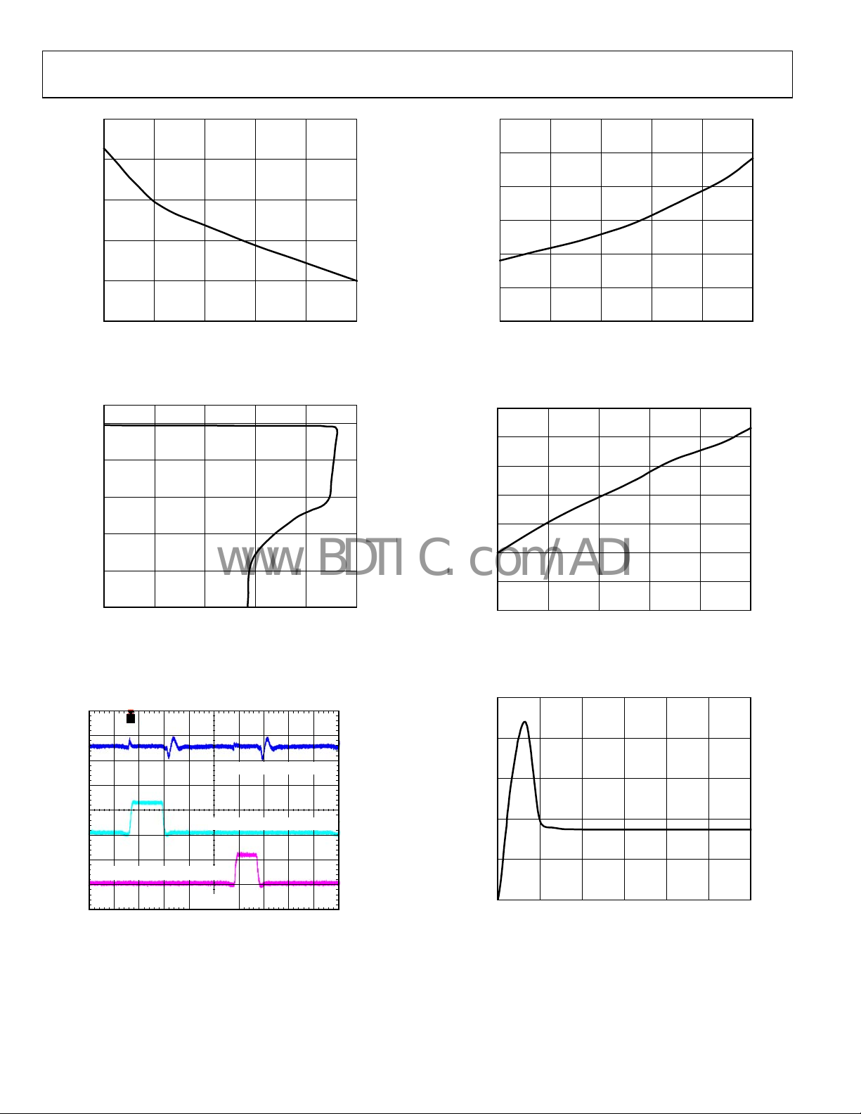
Figure 10. VREG vs. Load Current, V
= 12 V
IN
0.6005
0.6000
0.5995
0.5990
FEEDBACK VOLT AGE (V)
0.5985
0.5980
–40 8 5
06784-010
Figure 13. Feedback Voltage vs. Temperature, V
330
320
310
300
290
FREQUENCY (Hz)
280
270
–15 10 35 60
TEMPERATURE (° C)
= 12 V
IN
06784-013
0
0 50 100 150 200 250
LOAD CURRENT (mA)
Figure 11. VREG Current-Limit Foldback
T
VREG, AC-COUPLED, 1V/DIV
SW2 PIN, V
= 1.2V, 10V/DIV
OUT
SW1 PIN, V
200ns/DIV
= 1.8V, 10V/DIV
OUT
Figure 12. VREG Output During Normal Operation
260
–40 85
06784-011
Figure 14. Switching Frequency vs. Temperature, V
5
4
3
2
SUPPLY CURRENT (mA)
1
06784-012
0
22
–15103560
TEMPERATURE ( °C)
= 12 V
IN
5 8 11 14 17
SUPPLY VOLTAGE (V)
06784-014
0
06784-015
Figure 15. Supply Current vs. Input Voltage
Rev. 0 | Page 10 of 32
 Loading...