Synchronous Buck PWM,
V
V
FEATURES
Wide bias voltage range 3.0 V to 18 V
Wide power stage input range 1 V to 24 V
Wide output voltage range: 0.6 V to 85% of input voltage
±0.85% accuracy at 0
All N-channel MOSFET design for low cost
Fixed-frequency operation at 300 kHz, 600 kHz, or resistor
adjustable 300 kHz to 600 kHz
Clock output for synchronizing other controllers
No current sense resistor required
Internal linear regulator
Voltage tracking for sequencing
Soft start and thermal overload protection
Overvoltage and undervoltage power-good indicator
15 μA shutdown supply current
Available in a 20-lead QSOP
APPLICATIONS
Telecom and networking systems
Base station power
Set-top boxes, game consoles
Printers and copiers
Medical imaging systems
DSP and microprocessor core power supplies
DDR termination
GENERAL DESCRIPTION
The ADP1828 is a versatile and synchronous PWM voltage
mode buck controller. It drives an all N-channel power stage
o
C to 70oC
R6
100kΩ
C2
33pF
20kΩ
C3
5.6nF
C5
1µF
VREG
IN
C6
1µF
R8
C
SS
200nF
EN
FREQ
SYNC
PGOOD
COMP
SS
C7
1µF
PV TRK
ADP1828
GND
AGND
CLKOUT
CLKSET
BST
DH
SW
CSL
DL
PGND
FB
Step-Down, DC-to-DC Controller
ADP1828
to regulate an output voltage as low as 0.6 V to 85% of the input
voltage and is sized to handle large MOSFETs for point-of-load
regulators. The ADP1828 is ideal for a wide range of high power
applications, such as DSP and processor core I/O power, and
general-purpose power in telecommunications, medical imaging,
PC, gaming, and industrial applications. It operates from input
bias voltages of 3 V to 18 V with an internal LDO that generates
a 5 V output for input bias voltages greater than 5.5 V.
The ADP1828 operates at a pin-selectable, fixed switching
frequency of either 300 kHz or 600 kHz, or at any frequency
between 300 kHz and 600 kHz with a resistor. The switching
frequency can also be synchronized to an external clock up to
2× the part’s nominal oscillator frequency. The clock output
can be used for synchronizing additional ADP1828s (or the
ADP1829 controllers), thus eliminating the need for an external
clock source. The ADP1828 includes soft start protection to
limit any inrush current from the input supply during startup,
reverse current protection during soft start for a precharged
output, as well as a unique adjustable lossless current-limit
scheme utilizing external MOSFET R
For applications requiring power-supply sequencing, the
ADP1828 provides a tracking input that allows the output
voltage to track during startup, shutdown, and faults. The
additional supervisory and control features include thermal
overload, undervoltage lockout, and power good.
The ADP1828 operates over the −40°C to +125°C junction
temperature range and is available in a 20-lead QSOP.
= 10V TO 18
IN
C
IN
180µF
×2
D1
C4
0.47µF
R
CL
1.8kΩ
M1
L1 = 0.82µH
M2
×2
20V
C
OUT2
1000µF
×2
PGNDAGND
C
OUT1
47µF
X5R
6.3V
OUTPUT
1.8V, 20A
R1
20kΩ
R2
10kΩ
R3
7.5kΩ
C1
680pF
DSON
sensing.
f
= 300kHz
SW
C
: SANYO, O SCON 20SP180M
IN
C
: SANYO, PO SCAP 2R5TPD1000M5
OUT2
L1: WURTH ELEKTRONIC, 0.82µH, 744355182
D1: BAT54
M1: INFINE ON, BSC080N03LS
M2: INFINE ON, 2 × BSC030N03LS
06865-001
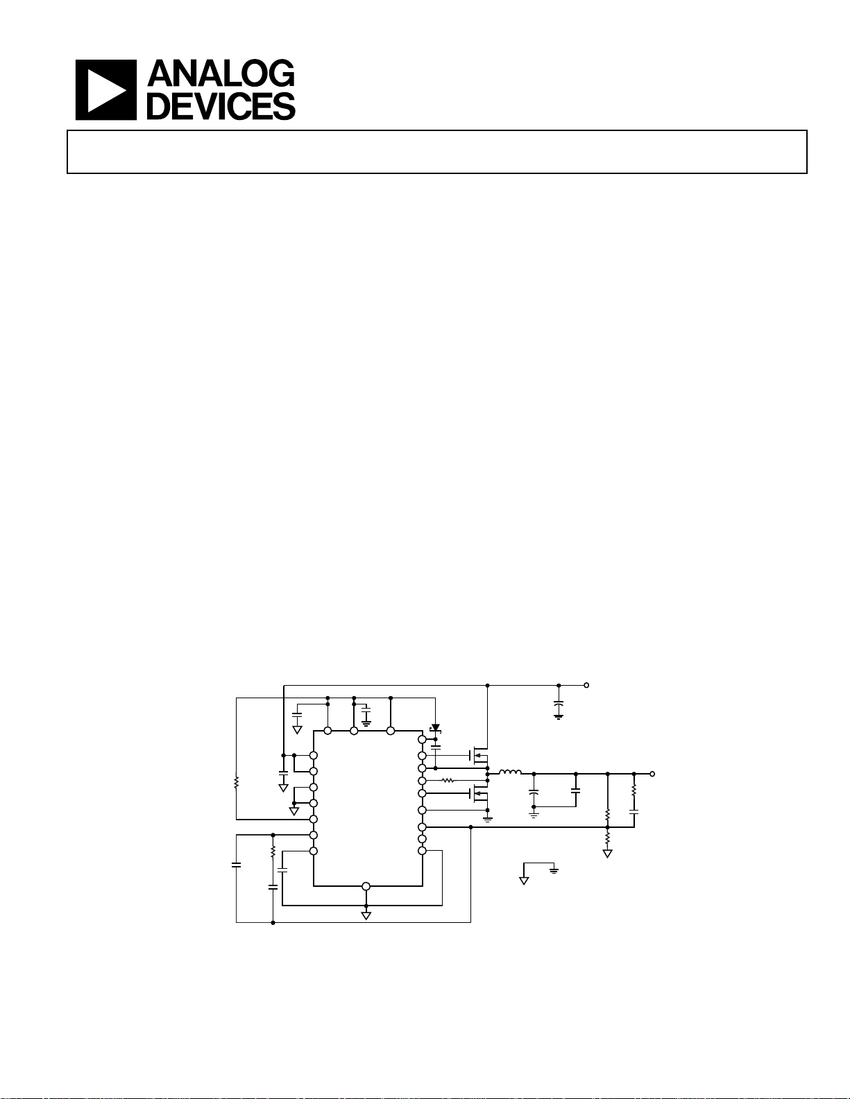
Figure 1. Typical Application Circuit with 20 A Output
Rev. 0
Information furnished by Analog Devices is believed to be accurate and reliable. However, no
responsibility is assumed by Analog Devi ces for its use, nor for any infringements of patents or other
rights of third parties that may result from its use. Specifications subject to change without notice. No
license is granted by implication or otherwise under any patent or patent rights of Analog Devices.
Trademarks and registered trademarks are the property of their respective owners.
One Technology Way, P.O. Box 9106, Norwood, MA 02062-9106, U.S.A.
Tel: 781.329.4700 www.analog.com
Fax: 781.461.3113 ©2007 Analog Devices, Inc. All rights reserved.

ADP1828
TABLE OF CONTENTS
Features .............................................................................................. 1
Applications ....................................................................................... 1
General Description ......................................................................... 1
Revision History ............................................................................... 2
Specifications ..................................................................................... 3
Absolute Maximum Ratings ............................................................ 6
ESD Caution .................................................................................. 6
Simplified Block Diagram ............................................................... 7
Pin Configuration and Function Descriptions ............................. 8
Typical Performance Characteristics ............................................. 9
Theory of Operation ...................................................................... 14
Input Power ................................................................................. 14
Internal Linear Regulator .......................................................... 14
Soft Start ...................................................................................... 14
Error Amplifier ........................................................................... 15
Current-Limit Scheme ............................................................... 15
MOSFET Drivers ........................................................................ 15
Setting the Output Voltage ........................................................ 16
Switching Frequency Control and Synchronization .............. 16
Compensation ............................................................................. 17
Power-Good Indicator ............................................................... 17
Thermal Shutdown ..................................................................... 17
Shutdown Control ...................................................................... 17
Tracking ....................................................................................... 17
Application Information ................................................................ 18
Selecting the Input Capacitor ................................................... 18
Output LC Filter ......................................................................... 18
Selecting the MOSFETs ............................................................. 19
Setting the Current Limit .......................................................... 20
Accurate Current-Limit Sensing .............................................. 20
Feedback Voltage Divider ......................................................... 20
Compensating the Voltage Mode Buck Regulator ................. 20
Soft Start ...................................................................................... 24
Switching Noise and Overshoot Reduction ............................ 24
Voltage Tracking ......................................................................... 24
Coincident Tracking .................................................................. 25
Ratiometric Tracking ................................................................. 25
Thermal Considerations ............................................................ 27
PCB Layout Guideline ................................................................... 28
Recommended Component Manufacturers ........................... 29
Application Circuits ....................................................................... 30
Outline Dimensions ....................................................................... 32
Ordering Guide .......................................................................... 32
REVISION HISTORY
9/07—Revision 0: Initial Version
Rev. 0 | Page 2 of 32
ADP1828
SPECIFICATIONS
IN = 12 V, PV = VEN = V
lation using standard statistical quality control (SQC). T
Table 1.
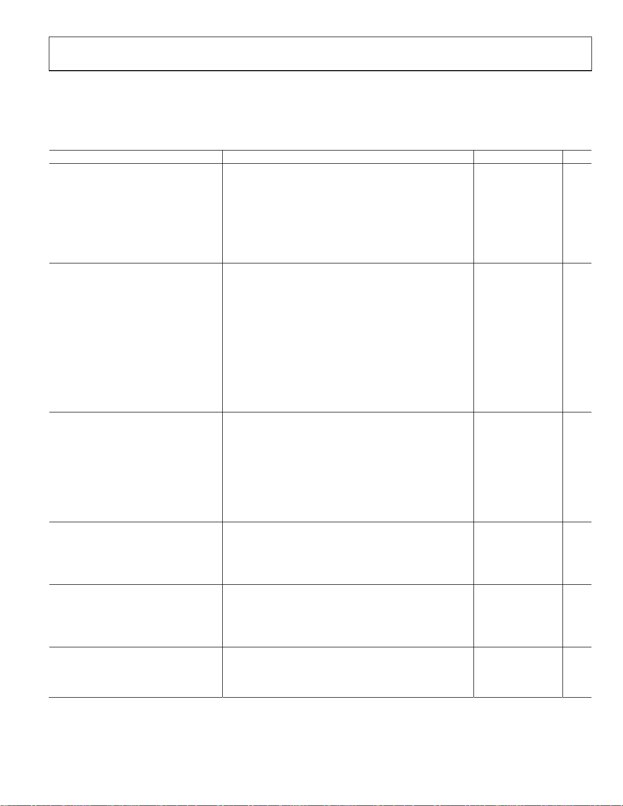
Parameter Conditions Min Typ Max Unit
POWER SUPPLY
IN Input Voltage PV is tied to VREG, IN is not tied to VREG (using internal regulator) 5.5 18 V
IN Input Voltage IN = PV = VREG, IN is tied to VREG (not using internal regulator) 3.0 5.5 V
IN Quiescent Current Not switching, I
IN Shutdown Current EN = GND 5 15 A
VREG-to-GND Shutdown Impedance EN = GND, IN is not tied to VREG 1.6 MΩ
VREG Undervoltage Lockout Threshold VREG rising 2.4 2.7 3.0 V
VREG Undervoltage Lockout Hysteresis VREG falling 0.125 V
ERROR AMPLIFER
FB Regulation Voltage TA = 25°C, TRK > 700 mV 597 600 603 mV
T
T
FB Input Bias Current 5 100 nA
Open-Loop Voltage Gain 70 dB
Gain-Bandwidth Product 20 MHz
COMP Sink Current 600 µA
COMP Source Current 120 µA
COMP Clamp High Voltage IN = VREG = 3V 2.4 V
IN = 12 V 3.6 V
COMP Clamp Low Voltage 0.75 V
LINEAR REGULATOR
VREG Output Voltage
VREG Load Regulation I
VREG Line Regulation IN = 5 V+ dropout voltage to 18 V, no load 1 mV
VREG Current Limit VREG drops to 4 V 220 mA
VREG Short-Circuit Current VREG drops to 0.4 V 60 140 200 mA
IN to VREG Dropout Voltage
VREG Minimum Output Capacitance 1 F
PWM CONTROLLER
VRAMP Peak-to-Peak Voltage
DH Maximum Duty Cycle FREQ = GND (300 kHz) 91 93 %
DH Minimum On Time Any frequency 100 ns
DL Minimum On Time Any frequency 200 ns
SOFT START
SS Pull-Up Resistance SS = GND 90 kΩ
SS Pull-Down Resistance SS = 0.6 V 6 kΩ
SS to FB Offset Voltage SS = 0 mV to 500 mV −45 mV
SS Pull-Up Voltage 0.8 V
TRACKING
TRK Common-Mode Input Voltage Range 0 600 mV
TRK to FB Offset Voltage TRK = 0 mV to 500 mV −5.5 +5 mV
TRK Input Bias Current 100 nA
= 5 V, SYNC = GND, unless otherwise specified. All limits at temperature extremes are guaranteed via corre-
TRK
= −40°C to +125°C, unless otherwise specified. Typical values are at TA = 25°C.
J
= 0 mA 1.5 3.0 mA
VREG
= 0°C to +70°C, TRK > 700 mV 595 605 mV
A
= −40°C to +125°C, TRK > 700 mV 591 609 mV
J
IN = 5 V+ dropout voltage to 18 V, I
= −40°C to +125°C
T
J
= 0 mA to 100 mA, IN = 5.25 V to 18 V −10 mV
VREG
1
2
I
= 100 mA, IN < 5 V 0.6 1.0 V
VREG
0.7 1.0 1.45 V
=100 mA
VREG
4.75 5.0 5.25 V
Rev. 0 | Page 3 of 32

ADP1828
Parameter Conditions Min Typ Max Unit
OSCILLATOR
Oscillator Frequency SYNC = FREQ = GND 240 300 360 kHz
SYNC = GND, FREQ = VREG 480 600 720 kHz
R
R
R
SYNC Synchronization Range FREQ = GND 300 600 kHz
FREQ = VREG 600 1200 kHz
SYNC Input Pulse Width 200 ns
SYNC Pin Capacitance 5 pF
CURRENT SENSE
CSL Threshold Voltage Relative to PGND −17 −38 −58 mV
CSL Output Current CSL = PGND 42 50 56 A
Current Sense Blanking Period 100 ns
GATE DRIVERS
DH Rise Time CDH = 3 nF, V
DH Fall Time CDH = 3 nF, V
DL Rise Time CDL = 3 nF 15 ns
DL Fall Time CDL = 3 nF 10 ns
DH or DL Driver RON, Sourcing Current
DH or DL Driver RON, Sinking Current
3, 4
3, 4
Sinking 1.5 A with a 0.1 µs pulse 1.5 Ω
DH or DL Driver RON, Sourcing Current IN = VREG = 3 V; sourcing 1 A with a 0.1 µs pulse 2.3 Ω
DH or DL Driver RON, Sinking Current IN = VREG = 3 V; sinking 1 A with a 0.1 µs pulse 2 Ω
DH to DL, DL to DH Dead Time 40 ns
CLOCK OUT
CLOCKOUT Pulse Width 360 ns
CLKOUT Rise or Fall Time C
SYNC to CLKOUT Propagation Delay, tPD C
SYNC to CLKOUT Propagation Delay, tPD C
LOGIC THRESHOLDS
SYNC, CLKSET, FREQ Logic High 1.8 V
SYNC, CLKSET Logic Low 0.4 V
FREQ Logic Low 0.25 V
CLKSET, SYNC, FREQ Input Leakage
Current
EN Input Threshold 1.1 1.5 1.8 V
EN Input Threshold Hysteresis 0.2 V
EN Current Source EN = 0 V to 3.0 V −0.1 −0.6 −1.5 A
EN Input Impedance to 5 V Zener EN = 5.5 V to 18 V 100 kΩ
THERMAL SHUTDOWN
Thermal Shutdown Threshold
4
Thermal Shutdown Hysteresis4 15 °C
= 57.6 kΩ 240 300 360 kHz
FREQ
= 35.7 kΩ 370 450 530 kHz
FREQ
= 24.9 kΩ 480 600 720 kHz
FREQ
− VSW = 5 V 15 ns
BST
− VSW = 5 V 10 ns
BST
Sourcing 1.5 A with a 0.1 µs pulse 2 Ω
= 47 pF 10 ns
CLKOUT
CLKOUT
CLKOUT
= 47 pF, C
= 47 pF, C
= 5 pF 40 ns
SYNC
= 5 pF, IN < 5 V 52 ns
SYNC
CLKSET, SYNC, FREQ = 0 V or VREG 1 A
145 °C
Rev. 0 | Page 4 of 32
ADP1828
Parameter Conditions Min Typ Max Unit
POWER GOOD
FB Overvoltage Threshold VFB rising 700 750 810 mV
FB Overvoltage Hysteresis 50 mV
FB Undervoltage Threshold VFB falling 500 550 585 mV
FB Undervoltage Hysteresis 50 mV
PGOOD Propagation Delay 8 s
PGOOD Off Leakage Current V
PGOOD Output Low Voltage I
1
Connect IN to VREG when IN < 5.5 V. For applications with IN < 5.5V and IN not connected to VREG, keep in mind that VREG = VIN – dropout. VREG needs to be ≥ 3 V for
proper operation.
2
V
= 1.0 V × f
RAMP
then fSW = f
3
With a 5 V drive, the peak source or sink current could be up to 2.5 A and 3.3 A, respectively, when driving external power MOSFETs. The duration of the peak current
pulse is generally in the order of 10 ns.
4
Guaranteed by design and characterization. Not subject to production test.
SYNC
OSC/fSW
.
, where f
is the natural oscillator frequency and fSW is the actual switching frequency. If SYNC is not used, then f
OSC
= 5.5 V 1 A
PGOOD
= 10 mA 150 500 mV
PGOOD
= fSW. If SYNC is used,
OSC
Rev. 0 | Page 5 of 32
ADP1828
ABSOLUTE MAXIMUM RATINGS
Table 2.
Parameter Rating
IN, TRK −0.3 V to +20 V
EN −0.3 V < IN + 0.3 V
PV, SYNC, FREQ, COMP, SS, FB, PGOOD,
−0.3 V to +6 V
CLKSET, CLKOUT, VREG
BST-to-GND, SW-to-GND −0.3 V to +30 V
BST-to-SW −0.3 V to +6 V
BST-to-GND, SW-to-GND, 50 ns transients +38 V
SW-to-GND, 30 ns negative transients −7 V
CSL-to-GND −1 V to +30 V
DH-to-GND
(SW − 0.3 V) to
(BST + 0.3 V)
DL-to-PGND
−0.3 V to
(PV + 0.3 V)
PGND-to-GND ±2 V
θJA, 20-Lead QSOP on a Multilayer PCB
(Natural Convection)
1
83°C/W
Operating Junction Temperature2 −40°C to +125°C
Storage Temperature −65°C to +150°C
Maximum Soldering Lead Temperature 260°C
1
Junction-to-ambient thermal resistance (θJA) of the package was calculated
or simulated on a multilayer PCB.
2
The ADP1828 can be damaged when the junction temperature limits are
exceeded. Monitoring ambient temperature does not guarantee that TJ
is within the specified temperature limits. In applications with moderate
power dissipation and low PCB thermal resistance, the maximum ambient
temperature can exceed the maximum limit as long as the junction temperature is within specification limits. The junction temperature, TJ, of the
device is dependent on the ambient temperature, TA, the power dissipation
of the device, PD, and the junction to ambient thermal resistance of the
package, θJA. Maximum junction temperature is calculated from the ambient
temperature and power dissipation using the formula TJ = TA + PD × θJA.
Stresses above those listed under Absolute Maximum Ratings
may cause permanent damage to the device. This is a stress
rating only; functional operation of the device at these or any
other conditions above those indicated in the operational
section of this specification is not implied. Exposure to absolute
maximum rating conditions for extended periods may affect
device reliability.
Absolute maximum ratings apply individually only, not in
combination. Unless otherwise specified all other voltages
are referenced to GND.
ESD CAUTION
Rev. 0 | Page 6 of 32
ADP1828
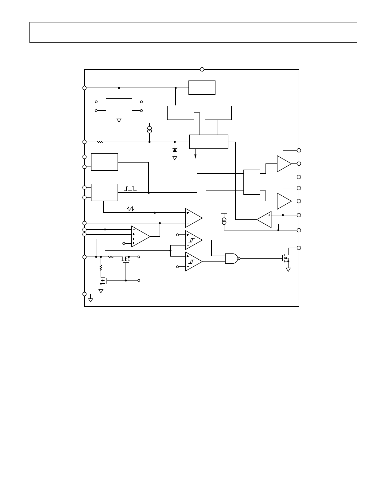
SIMPLIFIED BLOCK DIAGRAM
IN
ADP1828
VREG
0.6V
0.8V
REF
0.75V
0.55V
UVLO
IN
LINEAR
REG
THERMAL
SHUTDOWN
EN
CLKOUT
CLKSET
FREQ
SYNC
COMP
FB
TRK
SS
GND
100kΩ
CLKOUT
DRIVER
OSCILLAT OR
90kΩ
6kΩ
0.6V
RAMP
CLK
0.8V
FAULT
FAULT
PWM
COMPARATOR
0.75V
ERROR
AMPLIFIER
0.55V
Figure 2. Simplified Block Diagram
LOGIC
50µA
VREG
R
ILIM
PWM
BST
DH
QS
Q
SW
PV
DL
PGND
CSL
PGOOD
06865-003
Rev. 0 | Page 7 of 32
ADP1828
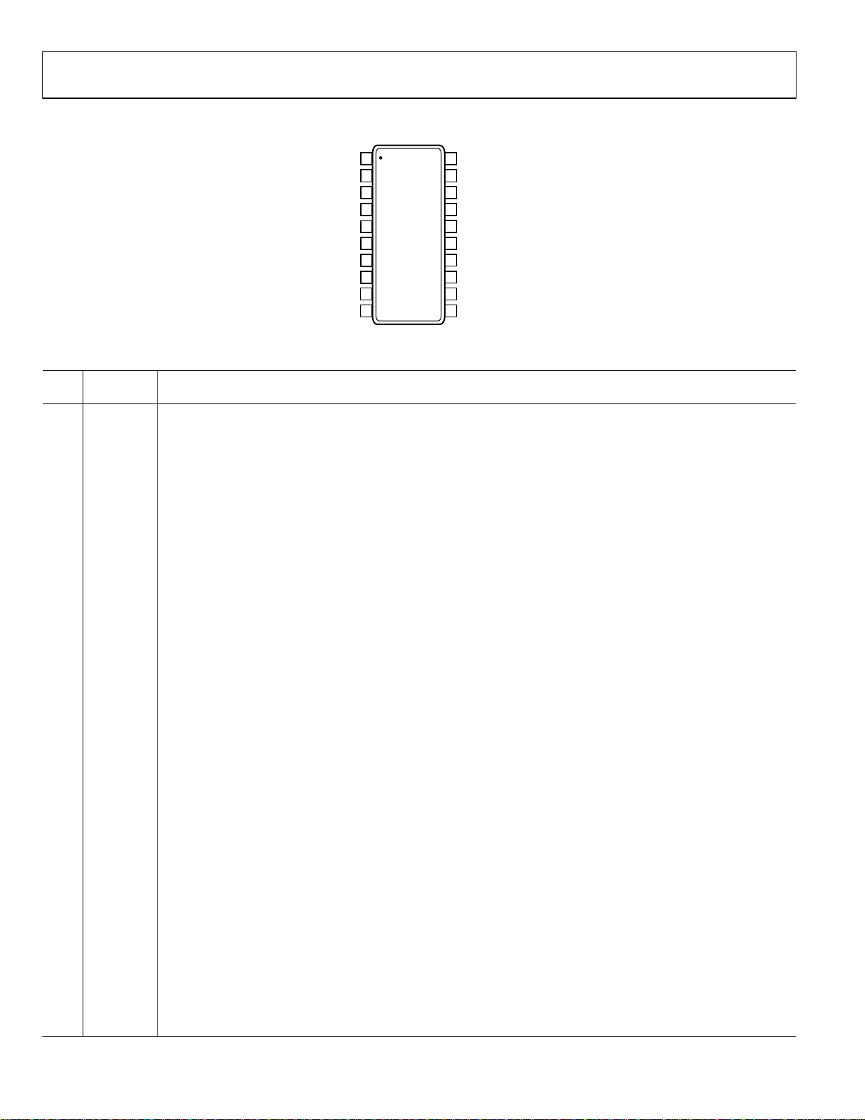
PIN CONFIGURATION AND FUNCTION DESCRIPTIONS
FREQ
SYNC
EN
VREG
GND
COMP
FB
TRK
SS
IN
1
2
3
ADP1828
4
TOP VIEW
5
(Not to Scale)
6
7
8
9
10
20
19
18
17
16
15
14
13
12
11
CLKOUT
CLKSET
BST
DH
SW
CSL
PGND
DL
PV
PGOOD
06865-004
Figure 3. Pin Configuration
Table 3. Pin Function Descriptions
Pin
No.
Mnemonic Description
1 FREQ
Frequency Control Input. Low for 300 kHz, high for 600 kHz, or connect a resistor from FREQ to GND to set the freerunning frequency between 300 kHz and 600 kHz.
2 SYNC
Frequency Synchronization Input. Accepts external signals between 300 kHz and 600 kHz if FREQ is set to low, or
between 600 kHz and 1.2 MHz if FREQ is set to high. If f
from f
up to 600 kHz. If SYNC is not used, connect SYNC to GND or VREG. V
OSC
is set by R
OSC
, then the synchronization frequency range is
FREQ
can be driven up to 6 V even when VIN
SYNC
is less than 6 V.
3 EN
Enable Input. Drive EN high or tristate EN to turn on the ADP1828 controller, and drive it low to turn off. Connect EN to
IN for automatic startup.
4 IN
Input Supply to the Internal Linear Regulator. Drive IN with 5.5 V to 18 V to power the ADP1828 from LDO, VREG; tie PV
to VREG. For input voltages between 3 V and 5.5 V, tie IN, PV, and VREG together.
5 VREG
Output of the Internal Linear Regulator (LDO). The internal circuitry and gate drivers are powered from VREG. Bypass
VREG to AGND plane with 1 F ceramic capacitor for stable operation, for example, a 10 V X5R 1 F ceramic capacitor
is sufficient. The VREG output is 5 V when IN = 5 V + dropout. Connect IN to VREG and PV when IN = 3 V to 5.5 V. For
applications with IN < 5.5 V and IN not connected to VREG, keep in mind that VREG = VIN – dropout. VREG needs to be
≥3 V for proper operation.
6 GND Ground for Internal Circuits. Tie the bottom of the feedback dividers to this GND.
7 COMP Error Amplifier Output. Connect an RC network from COMP to FB for loop compensation.
8 FB
Voltage Feedback. Connect a resistor divider from the buck regulator output to GND and tie the tap to FB to set the
output voltage.
9 TRK
Tracking Input. To track a master voltage, drive TRK from a voltage divider from the master voltage. If the tracking
function is not used, connect TRK to VREG.
10 SS Soft Start Control Input. Connect a capacitor from SS to GND to set the soft start period.
11 PGOOD
Open-Drain Power-Good Output. Sinks current when FB is out of regulation. Connect a pull-up resistor from
PGOOD to VREG.
12 PV
Positive Input Voltage for Gate Driver DL. When IN is 3 V to 5.5 V, connect IN to VREG and PV. Connect a 1 F bypass
capacitor from PV to PGND. When IN = 5.5 V to 18 V, connect PV to VREG.
13 DL Low-Side (Synchronous Rectifier) Gate Driver Output.
14 PGND Power GND. Ground for gate driver.
15 CSL Current Sense Comparator Inverting Input. Connect a resistor between CSL and SW to set the current-limit offset.
16 SW Switch Node Connection.
17 DH High-Side (Switch) Gate Driver Output.
18 BST
Boost Capacitor Input. Powers the high-side gate driver DH. Connect a 0.22 F to 0.47 F ceramic capacitor from BST
to SW and a Schottky diode from PV to BST.
19 CLKSET
Clock Set Input. Setting CLKSET to Logic high (connect CLKSET to VREG) sets the CLKOUT to 2× the internal oscillator
frequency and is in phase with the oscillator. Setting CLKSET to Logic low sets the CLKOUT to 1× the oscillator
frequency and 180° out of phase.
20 CLKOUT
Clock Output. The CLKOUT frequency, f
synchronize another ADP1828 or ADP1829 controllers. Set f
2× when synchronizing the ADP1829. If SYNC is used, f
, is either 1× or 2× the oscillator frequency. CLKOUT can be used to
CLKOUT
SYNC
to 1× when synchronizing another ADP1828, or to
CLKOUT
= f
independent of the CLKSET voltage. CLKOUT is
CLKOUT
able to drive a 100 pF load.
Rev. 0 | Page 8 of 32
ADP1828
TYPICAL PERFORMANCE CHARACTERISTICS
95
90
300kHz
80
70
60
EFFICIENCY (%)
50
40
30
02468101214161820
600kHz
LOAD (A)
VIN = 12V
= 1.8V
V
OUT
= 25°C
T
A
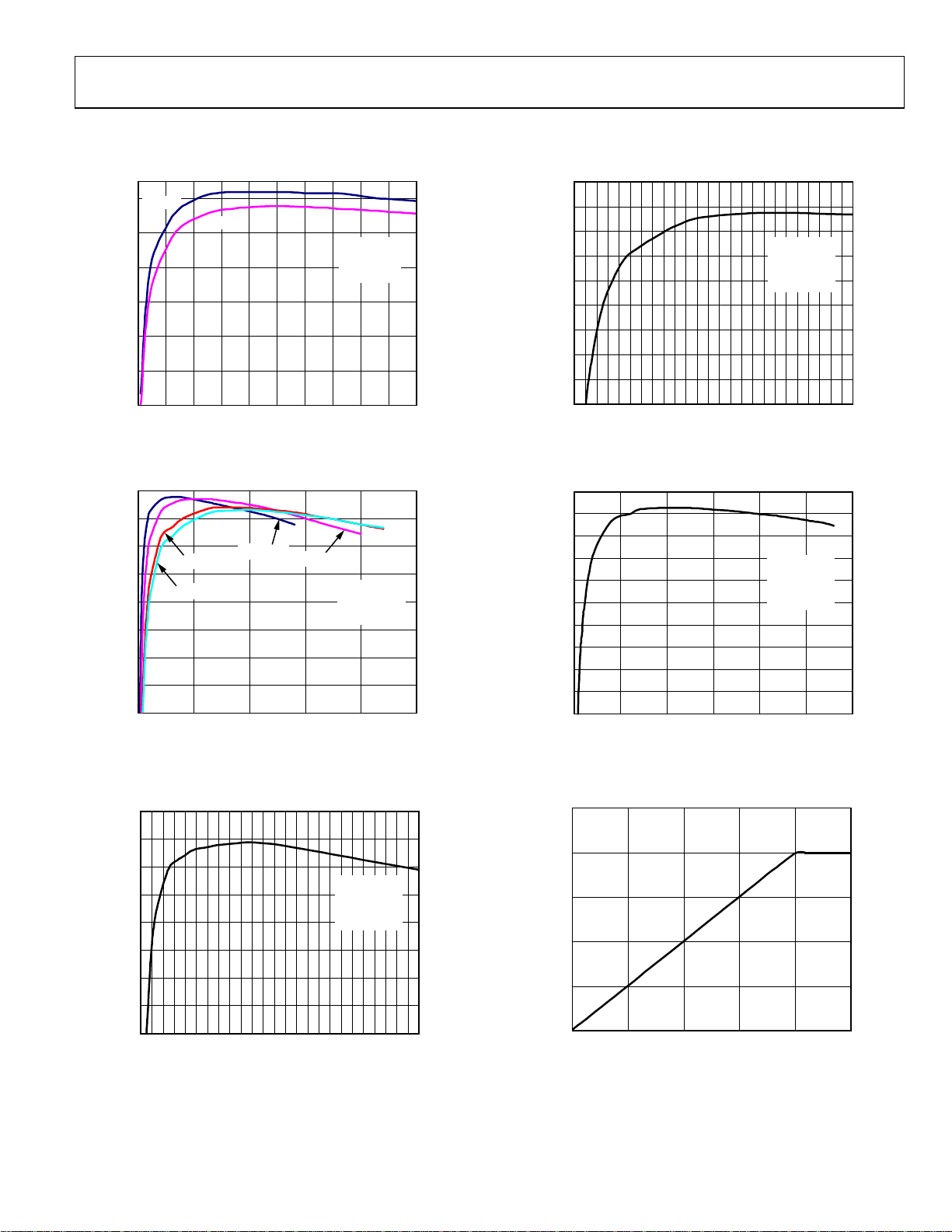
Figure 4. Efficiency vs. Load Current of Figure 1
06865-002
90
85
80
75
70
EFFICIENCY (%)
65
60
55
50
0123 45
LOAD (A)
fSW = 600kHz
= 12V
V
IN
= 3.3V
V
OUT
= 25°C
T
A
Figure 7. Efficiency vs. Load Current of Figure 54
06865-007
95
90
85
VIN = 12V
80
VIN = 15V
75
70
EFFICIENCY (%)
65
60
55
0 5 10 15 20 25
VIN = 3.3V
LOAD (A)
VIN = 5.5V
f
SW
V
OUT
T
A
= 25°C
= 300kHz
= 1.8V
Figure 5. Efficiency vs. Load Current of Figure 1
95
90
85
80
75
70
EFFICIENCY (%)
65
60
55
012345
LOAD (A)
fSW = 600kHz
= 3.3V
V
IN
= 1.2V
V
OUT
= 25°C
T
A
Figure 6. Efficiency vs. Load Current of Figure 53
95
90
85
80
75
70
65
EFFICIENCY (%)
60
55
50
45
06865-005
0 5 10 15 20 25 30
LOAD (A)
fSW = 300kHz
V
= 12V
IN
V
= 1.8V
OUT
T
= 25°C
A
06865-008
Figure 8. Efficiency vs. Load Current of Figure 56
5.5
T
= 25°C
A
5.0
4.5
4.0
VREG OUTPUT (V)
3.5
3.0
3.0 3.5 4.0 4.5 5.0 5.5
06865-006
V
(V)
IN
06865-009
Figure 9. VREG in Dropout, No Load
Rev. 0 | Page 9 of 32
ADP1828
5.000
4.995
4.990
4.985
4.980
4.975
4.970
VREG OUTPUT (V)
4.965
4.960
4.955
4.950
0 20 40 60 80 100
VREG LOAD CURRENT (mA)
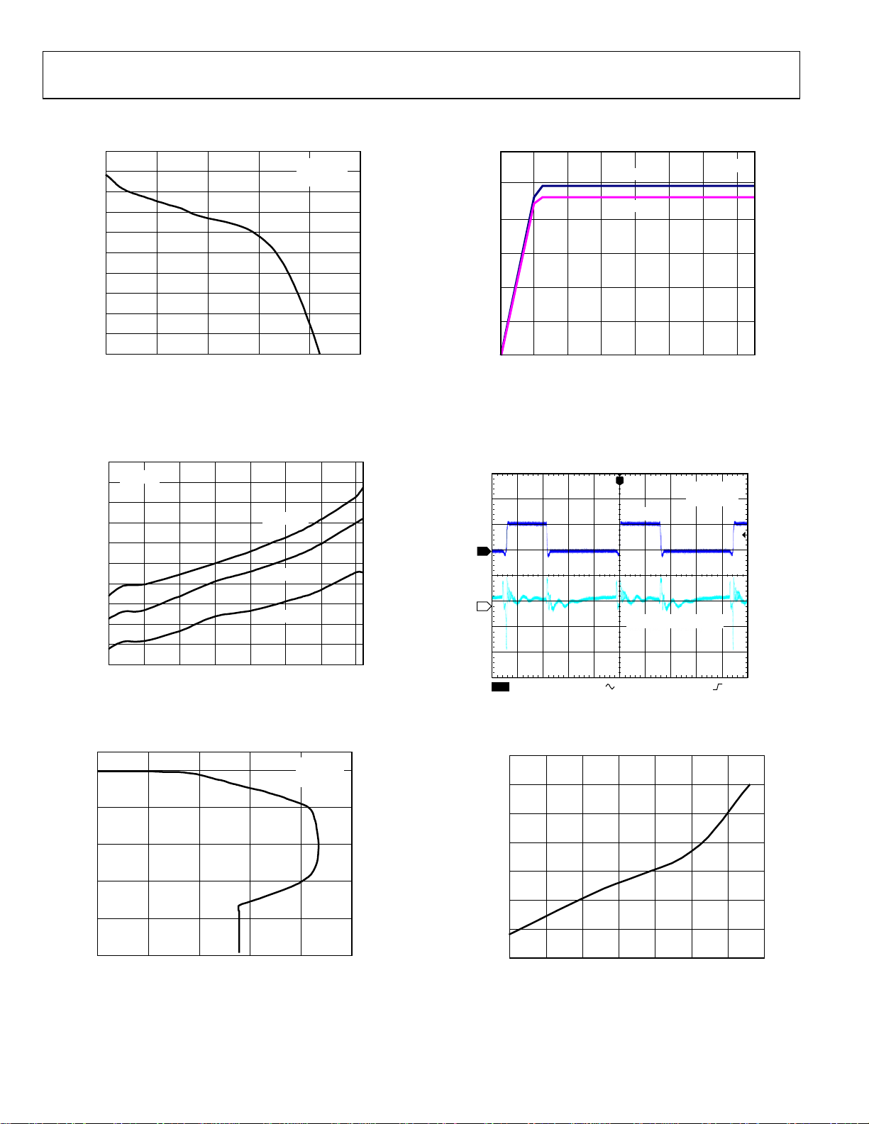
Figure 10. VREG vs. Load Current
5.000
VIN = 7V
4.995
4.990
4.985
4.980
4.975
VREG (V)
4.970
4.965
4.960
4.955
4.950
–50 –25 0 25 50 75 100 125
TEMPERATURE ( °C)
NO LOAD
10mA LOAD
100mA LOAD
Figure 11. VREG Voltage vs. Temperature
VIN = 5.5V
T
= 25°C
A
3.0
2.5
2.0
(%)
1.5
OSC
f
Δ
1.0
0.5
0
06865-010
3 5 7 9 11 13 15 17
Figure 13. Δ f
1
2
06865-011
CH1 5.00V CH2 100mV M 400ns A CH1 3. 60V
B
W
600kHz
300kHz
V
(V)
IN
vs. VIN, Referenced at VIN = 3 V
OSC
T
SW
VREG (AC-COUPLED)
B
W
TA = 25°C
VIN = 5.5V
LOAD = 5A
06865-013
06865-014
Figure 14. VREG Output of Figure 54
5
4
3
2
VREG OUTPUT (V)
1
0
0 50 100 150 200 250
VREG LOAD CURRENT (mA)
VIN = 5.5V
T
= 25°C
A
Figure 12. VREG Current-Limit Foldback
06865-012
Rev. 0 | Page 10 of 32
0.6025
0.6020
0.6015
0.6010
0.6005
0.6000
FEEDBACK VOLTAGE (V)
0.5995
0.5990
–40 –15 10 35 60 85 110 135
TEMPERATURE ( °C)
Figure 15. Feedback Voltage vs. Temperature, VIN = 12 V
06865-015
 Loading...