PWM, Step-Down DC-to-DC Controller
www.BDTIC.com/ADI
FEATURES
Wide power input voltage range: 1 V to 24 V
Chip supply voltage range: 3.7 V to 5.5 V
Wide output voltage range: 0.6 V to 85% of input voltage
1% accuracy, 0.6 V reference voltage
Output voltage margining control
Output voltage tracking
All N-channel MOSFET
300 kHz, 600 kHz, or up to 1.2 MHz synchronized frequency
No current sense resistor required
Power-good output
Programmable soft start with reverse current protection
Current-limit protection
Thermal overload protection
Overvoltage protection
Undervoltage lockout
1 μA shutdown supply current
Small, 24-lead QSOP package
APPLICATIONS
Telecommunications and networking systems
High performance servers
Medical imaging systems
DSP core power supplies
Microprocessor core power supplies
Mobile communication base stations
Distributed power
GENERAL DESCRIPTION
The ADP1822 is a versatile and inexpensive synchronous voltagemode PWM step-down controller. It drives an all N-channel power
stage to regulate an output voltage as low as 0.6 V.
BIAS INP UT
5V
15pF
Rev. C
Information furnished by Analog Devices is believed to be accurate and reliable. However, no
responsibility is assumed by Anal og Devices for its use, nor for any infringements of patents or ot her
rights of third parties that may result from its use. Specifications subject to change without notice. No
license is granted by implication or otherwise under any patent or patent rights of Analog Devices.
Trademarks and registered trademarks are the property of their respective owners.
1µF
80.6kΩ
309pF
10Ω
1µF
100nF
PVCC
BST
VCC
ADP1822
SHDN
FREQ
SYNC
PWGD
MAR
MSEL
COMP
SS
AGND DG ND
PGND
TRKP
TRKN
MDN
MUP
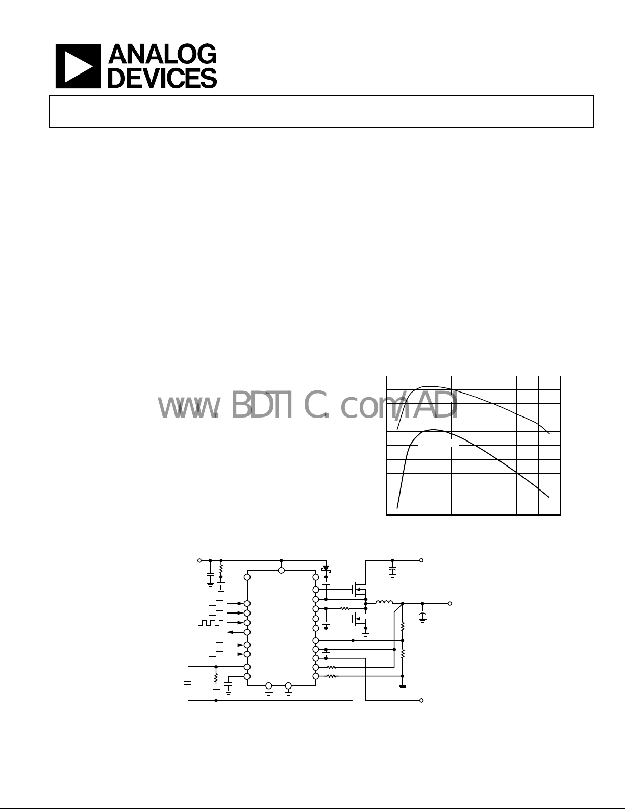
Figure 2. Typical Operating Circuit
DH
SW
CSL
DL
FB
with Margining and Tracking
ADP1822
The ADP1822 regulated output can track another power supply
and can be dynamically adjusted up or down with the controller’s
margining-control inputs, making it ideal for high reliability
applications. It is well suited for a wide range of high power
applications, such as DSP power and processor core power in
telecommunications, medical imaging, high performance
servers, and industrial applications. It operates from a 3.7 V to
5.5 V supply with power input voltage ranging from 1.0 V to 24 V.
The ADP1822 can operate at any frequency between 300 kHz
and 1.2 MHz, either by synchronizing with an external source
or an internally generated, logic-controlled clock of 300 kHz or
600 kHz. It includes an adjustable soft start to allow sequencing
and quick power-up while preventing input inrush current. Output
reverse-current protection at startup prevents excessive output
voltage excursions. The adjustable, virtually lossless currentlimit scheme reduces external part count and improves efficiency.
The ADP1822 operates over the −40°C to +125°C junction
temperature range and is available in a 24-lead QSOP package.
97
96
95
94
93
92
91
EFFICIENCY (%)
90
89
88
87
01
CMOSH-3
0.1µF
6.18kΩ
2.2pF
1nF
158kΩ
316kΩ
IRF3711
1µH
IRF3711
One Technology Way, P.O. Box 9106, Norwood, MA 02062-9106, U.S.A.
Tel: 781.329.4700 www.analog.com
Fax: 781.461.3113 ©2006–2007 Analog Devices, Inc. All rights reserved.
3.3V OUTPUT
1.8V OUTPUT
2 4 6 8 10 12 14
LOAD CURRENT (A)
Figure 1. Efficiency vs. Load Current, 5 V Input
POWER INPUT
2.25V TO 24V
180µF
20V
OUTPUT
1.8V, 15A
1000µF
4V
20kΩ
10kΩ
TRACKING
SIGNAL INPUT
05311-001
05311-006
6

ADP1822
www.BDTIC.com/ADI
TABLE OF CONTENTS
Features.............................................................................................. 1
Applications....................................................................................... 1
General Description ......................................................................... 1
Revision History ............................................................................... 2
Specifications..................................................................................... 3
Absolute Maximum Ratings............................................................ 5
ESD Caution.................................................................................. 5
Simplified Block Diagram ............................................................... 6
Pin Configuration and Function Descriptions............................. 7
Typical Performance Characteristics ............................................. 9
Theory of Operation ...................................................................... 12
Current-Limit Scheme............................................................... 12
Output Voltage Margining ........................................................ 12
Output Voltage Tracking ...........................................................12
Soft Start ...................................................................................... 12
High-Side Driver (BST and DH).............................................. 13
Low-Side Driver (DL)................................................................ 13
Input Voltage Range................................................................... 13
Setting the Output Voltage ........................................................ 13
Switching Frequency Control................................................... 13
Compensation............................................................................. 13
Power-Good Indicator............................................................... 13
Shutdown Control...................................................................... 13
Application Information................................................................ 14
Selecting the Input Capacitor................................................... 14
Output LC Filter......................................................................... 14
Selecting the MOSFETS ............................................................ 15
Setting the Current Limit.......................................................... 15
Feedback Voltage Divider ......................................................... 16
Setting the Voltage Margin........................................................ 16
Compensating the Regulator.................................................... 16
Setting the Soft Start Period...................................................... 18
Synchronizing the Converter.................................................... 19
Setting the Output Voltage Tracking ....................................... 19
Application Circuits ....................................................................... 20
Outline Dimensions....................................................................... 21
Ordering Guide .......................................................................... 21
REVISION HISTORY
5/07—Rev. B to Rev. C
Changes to Features.......................................................................... 1
Changes to General Description .................................................... 1
Changes to Specifications Section.................................................. 3
Changes to Table 2............................................................................ 5
Changes to Theory of Operation Section.................................... 12
Changes to Current Limit Scheme Section................................. 12
Changes to Setting the Current Limit Section............................ 15
Changes to Ordering Guide.......................................................... 21
8/06—Rev. A to Rev. B
Change to Title.................................................................................. 1
C
hange to General Description...................................................... 1
Changes to Figure 6.......................................................................... 9
Changes to Output Voltage Margining Section.......................... 12
Changes to Table 4.......................................................................... 12
1/06—Rev. 0 to Rev. A
Changes to Figure 1...........................................................................1
hanges to Table 1.............................................................................3
C
Changes to Input Voltage Range Section .................................... 13
Changes to Selecting the Input Capacitor Section..................... 14
Added Equation 1; Renumbered Sequentially ........................... 14
Changes to Equation 7 and Equation 8 ....................................... 15
Changes to Selecting the MOSFETS Section.............................. 15
Added Equation 9; Renumbered Sequentially ........................... 15
Changes to Equation 10................................................................. 15
Changes to Equation 22................................................................. 17
Changes to Compensating the Regulator Section...................... 17
Changes to Figure 19 and Figure 20............................................. 17
Changes to Equation 27................................................................. 17
Changes to Equation 34................................................................. 18
7/05—Revision 0: Initial Version
Rev. C | Page 2 of 24
ADP1822
www.BDTIC.com/ADI
SPECIFICATIONS
V
= V
VCC
correlation using standard statistical quality control (SQC). T
T
= 25°C.
A
Table 1.
Parameter Conditions Min Typ Max Unit
POWER SUPPLY
Input Voltage 3.7 5.5 V
Undervoltage Lockout Threshold V
V
Undervoltage Lockout Hysteresis V
Quiescent Current I
Shutdown Current
Power Stage Supply Voltage 1.0 24 V
ERROR AMPLIFER
FB Regulation Voltage TJ = −40°C to +85°C 594 600 606 mV
T
FB Input Bias Current –100 +1 +100 nA
Error Amplifier Open-Loop Voltage Gain 70 dB
COMP Output Sink Current 600 μA
COMP Output Source Current 110 μA
PWM CONTROLLER
PWM Peak Ramp Voltage 1.25 V
DL Minimum On Time FREQ = VCC (300 kHz) 120 170 220 ns
FREQ = VCC (300 kHz), TA=25°C 140 170 200 ns
SOFT START
SS Pull-Up Resistance SS = GND 95 kΩ
SS Pull-Down Resistance VSS = 0.6 V 1.65 2.5 4.2 kΩ
OSCILLATOR
Oscillator Frequency FREQ = GND 250 310 375 kHz
FREQ = VCC 470 570 720 kHz
Synchronization Range FREQ = GND 300 600 kHz
FREQ = VCC 600 1200 kHz
SYNC Minimum Pulse Width 80 ns
CURRENT SENSE
CSL Threshold Voltage Relative to PGND −30 0 +30 mV
CSL Output Current V
Current Sense Blanking Period 160 ns
GATE DRIVERS
DH Rise Time C
DH Fall Time C
DL Rise Time C
DL Fall Time C
Driver RON, Sourcing Current 1 A, 0.7 μs pulse 2 Ω
Driver RON, Sinking Current 1 A, 0.7 μs pulse 1.5 Ω
DL Low to DH High Dead Time 33 ns
DH Low to DL High Dead Time 42 ns
VOLTAGE MARGINING
High Output Voltage Margin Resistance MUP to FB, V
Low Output Voltage Margin Resistance MDN to FB, V
PVCC
= V
SHDN
= V
FREQ
= V
= 5 V, SYNC = MAR = MSEL = GND. All limits at temperature extremes are guaranteed via
TRKN
= −40°C to +125°C, unless otherwise specified. Typical values are at
J
rising, TJ = −40°C to +125°C 2.4 2.7 3.0 V
VCC
rising, TA = 25°C 2.5 2.7 2.9 V
VCC
0.1 V
VCC
+ I
, not switching 1 2 mA
VCC
VCC
= GND
SHDN
= −40°C to +125°C 588 600 606 mV
J
= 0 V 42 50 54 μA
CSL
= 3 nF, VDH = VIN, V
GATE
= 3 nF, VDH = VIN, V
GATE
= 3 nF, VDL = VIN 19 ns
GATE
= 3 nF, VDL = 0 V 13 ns
GATE
= V
MAR
= 5 V, V
MAR
− VSW = 5 V 16 ns
BST
− VSW = 5 V 12 ns
BST
= 5 V 20 Ω
MSEL
= 0 V 20 Ω
MSEL
10 μA
Rev. C | Page 3 of 24

ADP1822
www.BDTIC.com/ADI
Parameter Conditions Min Typ Max Unit
TRACKING
Tracking Comparator Input Offset –200 +200 mV
Tracking Comparator Delay 100 ns
Tracking Comparator Common-Mode Input Voltage Range 0 V
TRKP Pull-Up Resistance Pull-up to VCC 200 kΩ
TRKN Pull-Down Resistance 200 kΩ
LOGIC THRESHOLDS (SHDN, SYNC, FREQ, MAR, MSEL)
Input High Voltage V
Input Low Voltage V
SYNC, FREQ Input Leakage Current SYNC = FREQ = GND 0.1 1 μA
SHDN, MAR, MSEL Pull-Down Resistance
THERMAL SHUTDOWN
Thermal Shutdown Threshold 145 °C
Thermal Shutdown Hysteresis 10 °C
PWGD OUTPUT
FB Overvoltage Threshold VFB rising 750 mV
FB Overvoltage Hysteresis 35 mV
FB Undervoltage Threshold VFB rising 550 mV
FB Undervoltage Hysteresis 35 mV
PWGD Off Current V
PWGD Low Voltage I
= 3.7 V to 5.5 V 2.0 V
VCC
= 3.7 V to 5.5 V 0.8 V
VCC
100 kΩ
= 5 V 1 μA
PWGD
= 10 mA 150 500 mV
PWGD
V
VCC
Rev. C | Page 4 of 24
ADP1822
www.BDTIC.com/ADI
ABSOLUTE MAXIMUM RATINGS
Table 2.
Parameter Rating
VCC, SHDN
TRKP
MDN to GND; PVCC to PGND; BST to SW
BST to GND −0.3 V to +30 V
CSL to GND −1 V to +30 V
DH to GND
DL to PGND
SW to GND −2 V to +30 V
PGND to GND
θJA, 2-Layer (SEMI Standard Board) 122°C/W
θJA, 4-Layer (JEDEC Standard Board) 82°C/W
Operating Ambient Temperature Range −40°C to +85°C
Operating Junction Temperature Range −55°C to +125°C
Storage Temperature Range −65°C to +150°C
Maximum Soldering Lead Temperature 260°C
, SYNC, FREQ, COMP, SS, FB,
, TRKN, MAR, MSEL, MUP, and
−0.3 V to +6 V
− 0.3 V) to
(V
SW
+ 0.3 V)
(V
BST
−0.3 V to
(V
+ 0.3 V)
PVCC
±2 V
Stresses above those listed under Absolute Maximum Ratings
may cause permanent damage to the device. This is a stress
rating only; functional operation of the device at these or any
other conditions above those indicated in the operational
section of this specification is not implied. Exposure to absolute
maximum rating conditions for extended periods may affect
device reliability.
Absolute maximum ratings apply individually only, not in
combination. Unless otherwise specified, all other voltages are
referenced to GND.
ESD CAUTION
Rev. C | Page 5 of 24
ADP1822
www.BDTIC.com/ADI
SIMPLIFIED BLOCK DIAGRAM
SHDN
VCC
GND
FREQ
SYNC
COMP
MAR
MSEL
MUP
MDN
DGND
FB
SS
2.5kΩ
SHUTDOWN
OSCILLATOR
DECODE
100kΩ
THERMAL
V
FAULT
REF
REFERENCE
OV
UV0.8V
LOGICUVLO
FAU LT
S
Q
PWM
R
Q
VCC
UVLO
THSD
ADP1822
BST
DH
SW
PVCC
DL
PGND
CSL
TRKP
TRKN
PWGD
05311-002
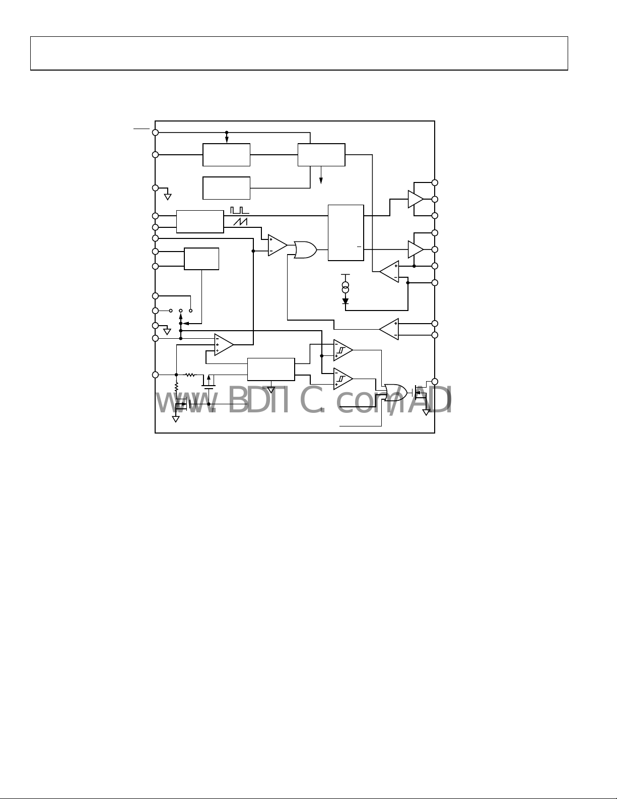
Figure 3. Simplified Block Diagram
Rev. C | Page 6 of 24
ADP1822
www.BDTIC.com/ADI
PIN CONFIGURATION AND FUNCTION DESCRIPTIONS
Table 3. Pin Function Descriptions
Pin No. Mnemonic Description
1 BST
High-Side Gate Driver Boost Capacitor Input. A capacitor between SW and BST powers the high-side gate driver
The capacitor is charged through a diode from PVCC when the low-side MOSFET is on. Connect a 0.1 μF or
DH.
greater ceramic capacitor from BST to SW and a Schottky diode from PVCC to BST to power the high-side gate
driver.
2 DH
High-Side Gate Driver Output. Connect DH to the gate of the external high-side N-channel MOSFET switch.
DH is powered from the capacitor between SW and BST and its voltage swings between V
3 SW
Power Switch Node. SW is the power switching node. Connect the source of the high-side N-channel MOSFET
switch and the drain of the low-side N-channel MOSFET synchronous rectifier to SW. SW powers the output
through the output LC filter.
4 SYNC
Frequency Synchronization Input. Drive SYNC with an external 300 kHz to 1.2 MHz signal to synchronize the
converter switching frequency to the applied signal. The maximum SYNC frequency is limited to 2× the nominal
internal frequency selected by FREQ. Do not leave SYNC unconnected; when not used, connect SYNC to GND.
5 FREQ
Frequency Select Input. FREQ selects the converter switching frequency. Drive FREQ low to select 300 kHz, or
high to select 600 kHz. Do not leave FREQ unconnected.
6 MAR
Margin Control Input. MAR is used with MSEL to control output voltage margining. MAR chooses between
high voltage and low voltage margining when MSEL is driven high. If not used, connect MAR to GND.
7 TRKN
Tracking Comparator Negative Input. Drive TRKN from the voltage that the ADP1822 output voltage tracks.
TRKN voltage is limited to VCC. See the Output Voltage Tracking section.
8 TRKP
Tracking Comparator Positive Input. Drive TRKP from the output voltage. TRKP voltage is limited to VCC.
See the Output Voltage Tracking section.
9
SHDN
Active Low DC-to-DC Shutdown Input. Drive SHDN high to turn on the converter. Drive it low to turn it off.
Connect SHDN
10 PWGD
Open-Drain Power-Good Output. PWGD sinks current to GND when the output voltage is above or below
the regulation voltage. Connect a pull-up resistor from PWGD to VDD for a logical power-good indicator.
11 DGND
12 GND
13 SS
Digital Ground. Connect DGND to GND at a single point as close as possible to the IC.
Analog Ground. Connect GND to PGND at a single point as close as possible to the IC.
Soft Start Control Input. A capacitor from SS to GND controls the soft start period. When the output is overloaded,
SS is discharged to prevent excessive input current while the output recovers. Connect a 1 nF to 1 μF capacitor
from SS to GND to set the soft start period. See the
14 FB
Voltage Feedback Input. Connect to a resistive voltage divider from the output to FB to set the output voltage.
See the Setting the Output Voltage section.
15 COMP
Compensation Node. Connect a resistor-capacitor network from COMP to FB to compensate the regulation
control system. See the Compensation section.
16 MSEL
Margin Select Input. Drive MSEL high to activate the voltage margining feature. Drive MSEL low to regulate
the output v
BST
DH
SW
SYNC
FREQ
MAR
TRKN
TRKP
SHDN
PWGD
DGND
GND
1
2
3
4
5
ADP1822
6
TOP VIEW
(Not to Scale)
7
8
9
10
11
12
NC = NO CONNECT
24
NC
23
PVCC
22
DL
21
PGND
20
CSL
19
VCC
18
MUP
17
MDN
16
MSEL
15
COMP
14
FB
13
SS
05311-005
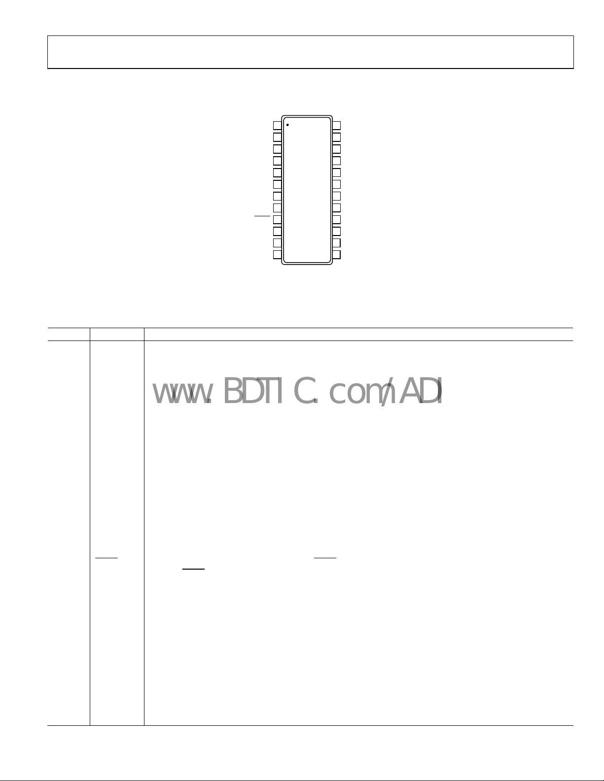
Figure 4. ADP1822 Pin Configuration
to VCC for automatic startup.
Soft Start section.
oltage to the nominal value. If not used, connect MSEL to GND.
and V
SW
BST
.
Rev. C | Page 7 of 24

ADP1822
www.BDTIC.com/ADI
Pin No. Mnemonic Description
17 MDN
18 MUP
19 VCC
20 CSL
21 PGND Power Ground. Connect GND to PGND at a single point as close as possible to the IC.
22 DL
23 PVCC
24 NC No Connection. Not internally connected.
Margin Down Input. Connect a resistor from MDN to the output
See the Setting the Voltage Margin section.
Margin Up Input. Connect a resistor from MUP to GND to set the high margining voltage. See the Setting the
ltage Margin section.
Vo
Internal Power Supply Input. VCC powers the in
connected as close as possible to the IC.
Low-Side Current Sense Input. Connect CSL to SW thr
urrent Limit section.
C
Low-Side Gate Driver Output. Connect DL to the gate of the low
The DL voltage swings between PGND and PVCC.
Internal Gate Driver Power Supply Input. PVCC powers the low-side gate driver DL. Bypass PVCC to PGND with 1
eater capacitor connected as close as possible to the IC.
μF or gr
ternal circuitry. Bypass VCC to GND with 0.1 μF or greater capacitor
ough a resistor to set the current limit. See the Setting the
voltage to set the low margining voltage.
-side N-channel MOSFET synchronous rectifier.
Rev. C | Page 8 of 24
 Loading...