ANALOG DEVICES ADP1821 Service Manual

www.BDTIC.com/ADI
Step-Down DC-to-DC Controller
FEATURES
Wide power-input voltage range: 1 V to 24 V
Chip supply voltage range: 3.7 V to 5.5 V
Wide output voltage range: 0.6 V to 85% of input voltage
1% accuracy, 0.6 V reference voltage
All N-channel MOSFET design for low cost
Fixed-frequency operation 300 kHz, 600 kHz, or
synchr
onized operation up to 1.2 MHz
No current sense resistor required
Power-good output
Programmable soft start with reverse current protection
Soft start, thermal overload, current-limit protection
Undervoltage lockout
10 μA shutdown supply current
Small, 16-lead QSOP
APPLICATIONS
Telecommunications and networking systems
Set-top boxes
Printers
Servers
Medical imaging systems
Microprocessor and DSP core power supplies
Mobile communication base stations
BIAS INPUT
5V
100kΩ
1.5nF
f
C
C
L1: COILTRONICS, HC7-1R0
1µF
10Ω
PVCC
VCC
1µF
= 300kHz
SW
IN2
OUT2
ADP1821
SHDN
FREQ
SYNC
PWGD
COMP
4.7kΩ
SS
GND
100nF
6.8nF
: SANYO, OSCON 20SP180M
: SANYO, OSCON 2R5SEPC820M
AGND
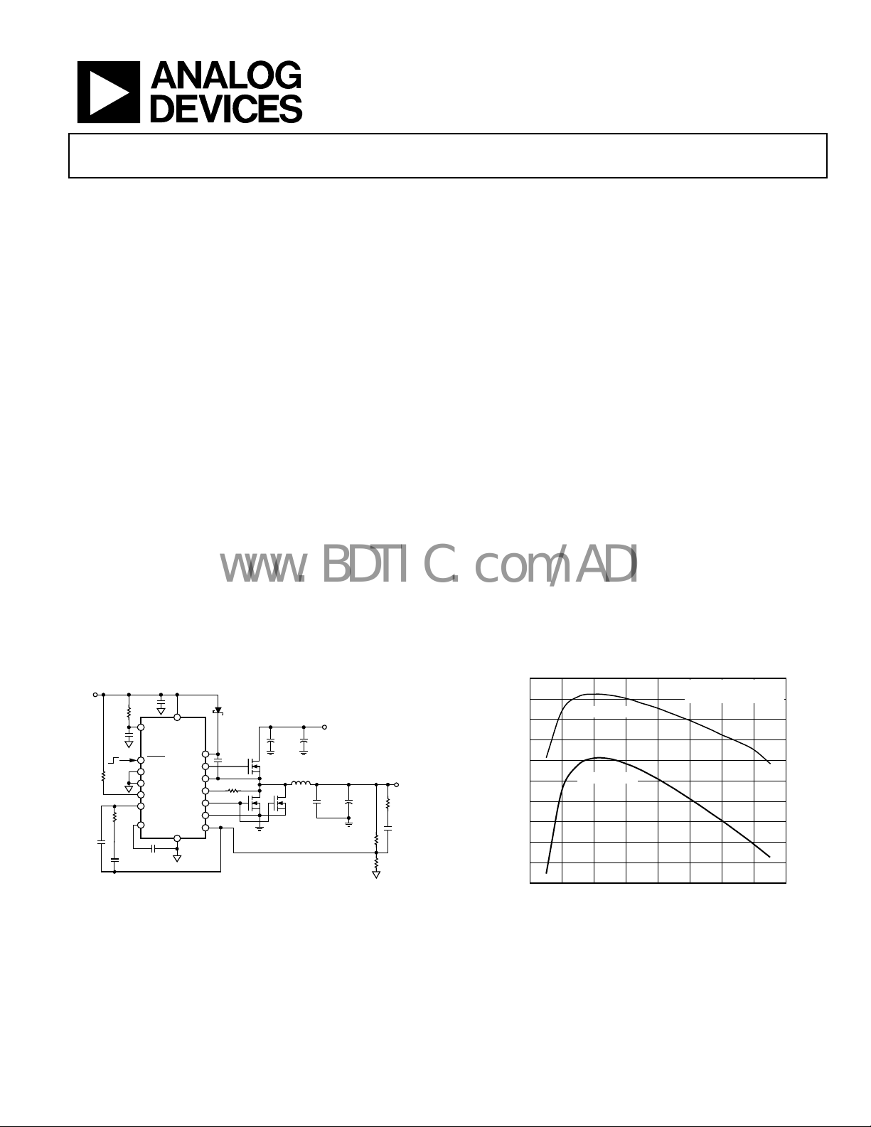
Figure 1. Typical Operating Circuit
BST
CSL
PGND
D1
0.47µF
DH
SW
3.3kΩ
DL
FB
C
: MURATA, GRM31MR71E225k
IN1
M1: IRLR7807Z
M2, M3: IRFR3709Z
D1: VISHAY BAT54
C
IN1
+
2.2µF
25V
M1
M2 M3
POWER INPUT
2.5V TO 20V
+
L1 = 1µH
C
IN2
2.2µF
25V
×2
C
10µF
6.3V
×2
OUT1
OUTPUT
1.8V, 20A
C
OUT2
+
820µF
2.5V
×2
2kΩ
1kΩ
300Ω
10nF
ADP1821
GENERAL DESCRIPTION
The ADP1821 is a versatile and inexpensive, synchronous,
pulse-width-modulated (PWM), voltage-mode, step-down
controller. It drives an all N-channel power stage to regulate an
output voltage as low as 0.6 V. The ADP1821 can be configured
to provide output voltages from 0.6 V to 85% of the input
voltage and is sized to handle large MOSFETs for point-of-load
regulators.
The ADP1821 is well suited for a wide range of high power
pplications, such as DSP and processor core power in telecom-
a
munications, medical imaging, high performance servers, and
industrial applications. It operates from a 3.7 V to 5.5 V supply
with a power input voltage ranging from 1.0 V to 24 V.
The ADP1821 operates at a pin-selectable, fixed switching
requency of either 300 kHz or 600 kHz, minimizing external
f
component size and cost. For noise sensitive applications, it
can be synchronized to an external clock to achieve switching
frequencies between 300 kHz and 1.2 MHz. The ADP1821
includes soft start protection to limit the inrush current from
the input supply during startup, reverse current protection
during soft start for precharged outputs, as well as a unique
adjustable lossless current-limit scheme utilizing external
MOSFET sensing.
The ADP1821 operates over the –40°C to +125°C junction
emperature range and is available in a 16-lead QSOP.
t
97
96
95
94
93
92
91
EFFICIENCY (%)
90
89
88
87
5310-001
0
3.3V OUTPUT
1.8V OUTPUT
2 4 6 8 10 12 14
LOAD CURRENT (A)
Figure 2. Efficiency vs. Load Current, 5 V Input
TA = 25°C
FREQUENCY = 300kHz
16
05310-002
Rev. C
Information furnished by Analog Devices is believed to be accurate and reliable. However, no
responsibility is assumed by Anal og Devices for its use, nor for any infringements of patents or ot her
rights of third parties that may result from its use. Specifications subject to change without notice. No
license is granted by implication or otherwise under any patent or patent rights of Analog Devices.
Trademarks and registered trademarks are the property of their respective owners.
One Technology Way, P.O. Box 9106, Norwood, MA 02062-9106, U.S.A.
Tel: 781.329.4700 www.analog.com
Fax: 781.461.3113 ©2005–2007 Analog Devices, Inc. All rights reserved.

ADP1821
www.BDTIC.com/ADI
TABLE OF CONTENTS
Features.............................................................................................. 1
Applications....................................................................................... 1
General Description ......................................................................... 1
Revision History ............................................................................... 2
Specifications..................................................................................... 3
Absolute Maximum Ratings............................................................ 5
ESD Caution.................................................................................. 5
Simplified Block Diagram ........................................................... 5
Pin Configuration and Function Descriptions............................. 6
Typical Performance Characteristics ............................................. 7
Theory of Operation ........................................................................ 9
Soft Start ........................................................................................ 9
Error Amplifier............................................................................. 9
Current-Limit Scheme................................................................. 9
MOSFET Drivers........................................................................ 10
Input Voltage Range ................................................................... 10
Setting the Output Voltage........................................................ 10
Switching Frequency Control and Synchronization.............. 10
Compensation............................................................................. 11
Power-Good Indicator............................................................... 11
Thermal Shutdown .................................................................... 11
Shutdown Control...................................................................... 11
Application Information................................................................ 12
Selecting the Input Capacitor................................................... 12
Output LC Filter......................................................................... 12
Selecting the MOSFETs ............................................................. 13
Setting the Current Limit.......................................................... 14
Feedback Voltage Divider ......................................................... 14
Compensating the Voltage Mode Buck Regulator................. 14
Setting the Soft Start Period...................................................... 18
PCB Layout Guideline ................................................................... 19
Recommended Component Manufacturers........................... 20
Application Circuits ....................................................................... 21
Outline Dimensions....................................................................... 23
Ordering Guide .......................................................................... 23
REVISION HISTORY
4/07—Rev. B to Rev. C
Changes to Specifications Section.................................................. 3
Changes to Absolute Maximum Ratings Section......................... 5
Changes to Current-Limit Scheme Section ................................ 10
Changes to Setting the Current Limit Section............................ 14
Added Figure 15.............................................................................. 14
Changes to Compensating the Voltage Mode Buck
Regu
lator Section............................................................................ 15
Changes to Type II Compensator Section................................... 17
Changes to Type III Compensator Section ................................. 18
Changes to Application Circuits Section..................................... 21
Changes to Figure 22...................................................................... 21
Changes to Ordering Guide.......................................................... 23
12/06—Rev. A to Rev. B
Updated Format..................................................................Universal
C
hanges to Features Section............................................................ 1
Changes to Applications Section .................................................... 1
Changes to General Description Section ...................................... 1
Changes to Error Amplifier............................................................. 3
Changes to PWM Controller.......................................................... 3
Changes to Oscillator Frequency.................................................... 3
Changes to Theory of Operation Section.......................................9
Changes to Application Information Section............................. 12
Added PCB Layout Section........................................................... 19
Changes to Application Circuits Section..................................... 21
Added Summary of Equations Section........................................ 23
1/06—Rev. 0 to Rev. A
C
hanges to Specifications Table ......................................................3
Changes to Theory of Operation Section.................................... 10
Changes to Input Voltage Range Section .................................... 11
Added Equation 1........................................................................... 12
Changes to Equation 7 and Equation 8 ....................................... 13
Added Equation 9........................................................................... 13
Changes to Equation 16................................................................. 14
Changes to Figure 15...................................................................... 14
Changes to Equation 21................................................................. 15
Changes to Figure 16...................................................................... 15
Changes to Equation 28................................................................. 15
Updated Outline Dimensions....................................................... 18
7/05—Revision 0: Initial Version
Rev. C | Page 2 of 24

ADP1821
www.BDTIC.com/ADI
SPECIFICATIONS
V
= V
VCC
statistical quality control (SQC). T
Table 1.
Parameter Conditions Min Typ Max Unit
POWER SUPPLY
Input Voltage 3.7 5.5 V
Undervoltage Lockout Threshold V
Undervoltage Lockout Threshold V
Undervoltage Lockout Hysteresis V
Quiescent Current I
Shutdown Current
Power Stage Supply Voltage 1.0 24 V
ERROR AMPLIFIER
FB Regulation Voltage TJ = −40°C to +85°C 594 600 606 mV
FB Regulation Voltage TJ = −40°C to +125°C 588 600 606 mV
FB Input Bias Current −100 +1 +100 nA
Error Amplifier Open-Loop Voltage Gain 70 dB
COMP Output Sink Current 600 A
COMP Output Source Current 110 A
COMP Clamp High Voltage 2.4 V
COMP Clamp Low Voltage 0.75 V
PWM CONTROLLER
PWM Peak Ramp Voltage 1.25 V
DL Minimum On Time FREQ = VCC (300 kHz) 120 170 220 ns
DL Minimum On-Time FREQ = VCC (300 kHz), TA = 25°C 140 170 200 ns
DH Maximum Duty Cycle FREQ = GND (300 kHz) 85 90 %
DH Minimum Duty Cycle FREQ = GND (300 kHz) 1 3 %
SOFT START
SS Pull-Up Resistance SS = GND 95 kΩ
SS Pull-Down Resistance VSS = 0.6 V 1.65 2.5 4.2 kΩ
OSCILLATOR
Oscillator Frequency FREQ = GND 250 310 375 kHz
FREQ = VCC 470 570 720 kHz
Synchronization Range FREQ = GND 300 600 kHz
FREQ = VCC 600 1200 kHz
SYNC Minimum Pulse Width 80 ns
CURRENT SENSE
CSL Threshold Voltage Relative to PGND −30 0 +30 mV
CSL Output Current V
Current Sense Blanking Period 160 ns
GATE DRIVERS
DH Rise Time C
DH Fall Time C
DL Rise Time C
DL Fall Time C
DL Low to DH High Dead Time 33 ns
DH Low to DL High Dead Time 42 ns
PVCC
= V
SHDN
= V
= 5 V, SYNC = GND. All limits at temperature extremes are guaranteed via correlation using standard
FREQ
= −40°C to +125°C, unless otherwise specified. Typical values are at TA=25°C.
J
rising, TJ = −40°C to +125°C 2.4 2.7 3.0 V
VCC
rising, TA = 25°C 2.5 2.7 2.9 V
VCC
0.1 V
VCC
+ I
, not switching 1 2 mA
VCC
VCC
= GND
SHDN
= 0 V 42 50 54
CSL
= 3 nF, VDH = VIN, V
GATE
= 3 nF, VDH = VIN, V
GATE
= 3 nF, VDL = VIN 19 ns
GATE
= 3 nF, VDL = 0 V 13 ns
GATE
− VSW = 5 V 16 ns
BST
− VSW = 5 V 12 ns
BST
10
A
μA
Rev. C | Page 3 of 24

ADP1821
www.BDTIC.com/ADI
Parameter Conditions Min Typ Max Unit
LOGIC THRESHOLDS (SHDN, SYNC, FREQ)
SHDN, SYNC, FREQ Input High Voltage
SHDN, SYNC, FREQ Input Low Voltage
SYNC, FREQ Input Leakage Current SYNC = FREQ = GND 0.1 1 A
SHDN Pull-Down Resistance
THERMAL SHUTDOWN
Thermal Shutdown Threshold 145 °C
Thermal Shutdown Hysteresis 10 °C
PWGD OUTPUT
FB Overvoltage Threshold VFB rising 750 mV
FB Overvoltage Hysteresis 35 mV
FB Undervoltage Threshold VFB rising 550 mV
FB Undervoltage Hysteresis 35 mV
PWGD Off Current V
PWGD Low Voltage I
V
= 3.7 V to 5.5 V 2.0
VCC
V
= 3.7 V to 5.5 V 0.8
VCC
100
= 5 V 1 A
PWGD
= 10 mA 150 500 mV
PWGD
V
V
kΩ
Rev. C | Page 4 of 24

ADP1821
C
www.BDTIC.com/ADI
ABSOLUTE MAXIMUM RATINGS
Table 2.
Parameter Rating
VCC, SHDN, SYNC, FREQ, COMP, SS, FB to
−0.3 V to +6 V
GND, PVCC to PGND, BST to SW
BST to GND −0.3 V to +30 V
CSL to GND −1 V to +30 V
DH to GND
DL to PGND
− 0.3 V) to
(V
SW
+ 0.3 V)
(V
BST
−0.3 V to
+ 0.3 V)
(V
PVCC
SW to GND −2 V to +30 V
PGND to GND ±2 V
θJA, 2-Layer (SEMI Standard Board) 150°C/W
θJA, 4-Layer (JEDEC Standard Board) 105°C/W
Operating Ambient Temperature Range −40°C to +85°C
Operating Junction Temperature Range −55°C to +125°C
Storage Temperature Range −65°C to +150°C
Maximum Soldering Lead Temperature 260°C
Stresses above those listed under Absolute Maximum Ratings
may cause permanent damage to the device. This is a stress
rating only; functional operation of the device at these or any
other conditions above those indicated in the operational
section of this specification is not implied. Exposure to absolute
maximum rating conditions for extended periods may affect
device reliability.
Absolute maximum ratings apply individually only, not in
mbination. Unless otherwise specified, all other voltages
co
are referenced to GND.
ESD CAUTION
SIMPLIFIED BLOCK DIAGRAM
SHDN
VCC
GND
FREQ
SYNC
OMP
FB
SS
SHUTDOWN
OSCILLAT OR
100kΩ
2.5kΩ
THERMAL
FAULT
LOGICUVLO
FAULT
S
PWM
R
VCC
OV0.6V
REFERENCE
UV0.8V
UVLO
THSD
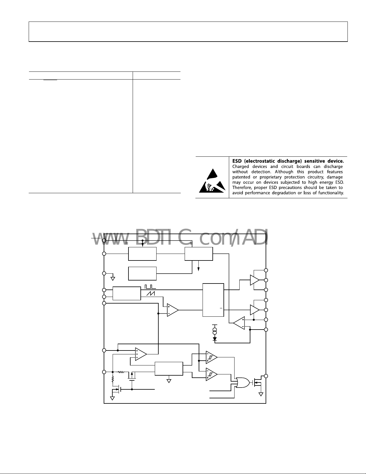
Figure 3. Simplified Block Diagram
ADP1821
BST
DH
Q
Q
SW
PVCC
DL
PGND
CSL
PWGD
05310-003
Rev. C | Page 5 of 24

ADP1821
www.BDTIC.com/ADI
PIN CONFIGURATION AND FUNCTION DESCRIPTIONS
1
BST
2
DH
3
SW
ADP1821
TOP VIEW
4
SYNC
FREQ
SHDN
PWGD
GND SS
(Not to Scale)
5
6
7
8
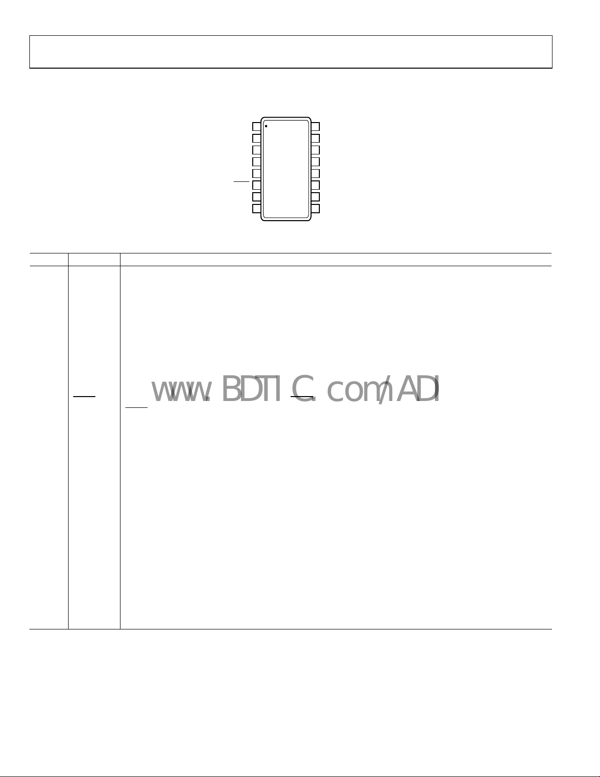
Figure 4. Pin Configuration
16
PVCC
15
DL
14
PGND
13
CSL
12
VCC
11
COMP
10
FB
9
05310-004
Table 3. Pin Function Descriptions
Pin No. Mnemonic Description
1 BST
High-Side Gate Driver Boost Capacitor Input. A capacitor between SW and BST powers the high-side gate driver, DH.
The capacit
or is charged through a diode from PVCC when the low-side MOSFET is on. Connect a 0.1 µF or greater
ceramic capacitor from BST to SW and a Schottky diode from PVCC to BST to power the high-side gate driver.
2 DH
3 SW
4 SYNC
High-Side Gate Driver Output. Connect DH to the gate of the ex
powered from the capacitor between SW and BST, and its voltage swings between V
Power Switch Node. Connect the source of the high-side, N-channel MOSFET switch and the drain of the low-side,
channel MOSFET synchronous rectifier to SW. SW powers the output through the output LC filter.
NFrequency Synchronization Input. Drive SYNC with an external 300 kHz to 1.2 MHz signal to synchronize the converter
switching fr
equency to the applied signal. The maximum SYNC frequency is limited to 2 times the nominal internal
ternal high-side, N-channel MOSFET switch. DH is
SW
and V
BST
.
frequency selected by FREQ. Do not leave SYNC unconnected; when not used, connect SYNC to GND.
5 FREQ
6
SHDN
Frequency Select Input. FREQ selects the converter switching frequency. Drive FREQ low to select 300 kHz, or high
t 600 kHz. Do not leave FREQ unconnected.
to selec
Active Low, DC-to-DC Shutdown Input. Drive SHDN high to turn on the converter and low to turn it off. Connect
SHDN to VCC for automatic startup.
7 PWGD
Open-Drain, Power-Good Output. PWGD sinks current to GND
when the output voltage is above or below the
regulation voltage. Connect a pull-up resistor from PWGD to VDD for a logical power-good indicator.
8 GND Analog Ground. Connect GND to PGND at a single point as close as possible to the internal circuitry (IC).
9 SS
Soft Start Control Input. A capacitor from SS to GND controls the soft start period. When the output is overloaded,
SS is dischar
ged to prevent excessive input current while the output recovers. Connect a 1 nF capacitor to a 1 µF
capacitor from SS to GND to set the soft start period. See the Soft Start section.
10 FB
Voltage Feedback Input. Connect to a resistive voltage divider from the output to FB to set the output v
the Setting the Output Voltage section.
11 COMP
12 VCC
Compensation Node. Connect a resistor-capacitor network from COMP to FB to compensate the regulation control
system. S
Internal Power Supply Input. VCC powers the in
ee the Compensation section.
ternal circuitry. Bypass VCC to GND with a 0.1 µF or greater
capacitor connected as close as possible to the IC.
13 CSL
Low-Side Current Sense Input. Connect CSL to SW thr
urrent Limit section.
C
ough a resistor to set the current limit. See the Setting the
14 PGND Power Ground. Connect GND to PGND at a single point as close as possible to the IC.
15 DL
Low-Side Gate Driver Output. Connect DL to the gate of the low
-side, N-channel MOSFET synchronous rectifier. The
DL voltage swings between PGND and PVCC.
16 PVCC
Internal Gate Driver Power Supply Input. PVCC powers the low-side gate driver, DL. Bypass PVCC to PGND with a
1 µF or gr
eater capacitor connected as close as possible to the IC.
oltage. See
Rev. C | Page 6 of 24

ADP1821
www.BDTIC.com/ADI
TYPICAL PERFORMANCE CHARACTERISTICS
97
96
95
94
93
92
91
EFFICIENCY (%)
90
89
88
87
0
3.3V OUTPUT
1.8V OUTPUT
2 4 6 8 10 12 14
LOAD CURRENT (A)
TA = 25°C
FREQUENCY = 300kHz
16
05310-005
0.6003
0.6002
0.6001
0.6000
0.5999
0.5998
FEEDBACK VOLT AGE (V)
0.5997
0.5996
–50
–30 –10 10 30 50 70 90
TEMPERATURE (° C)
110
05310-008
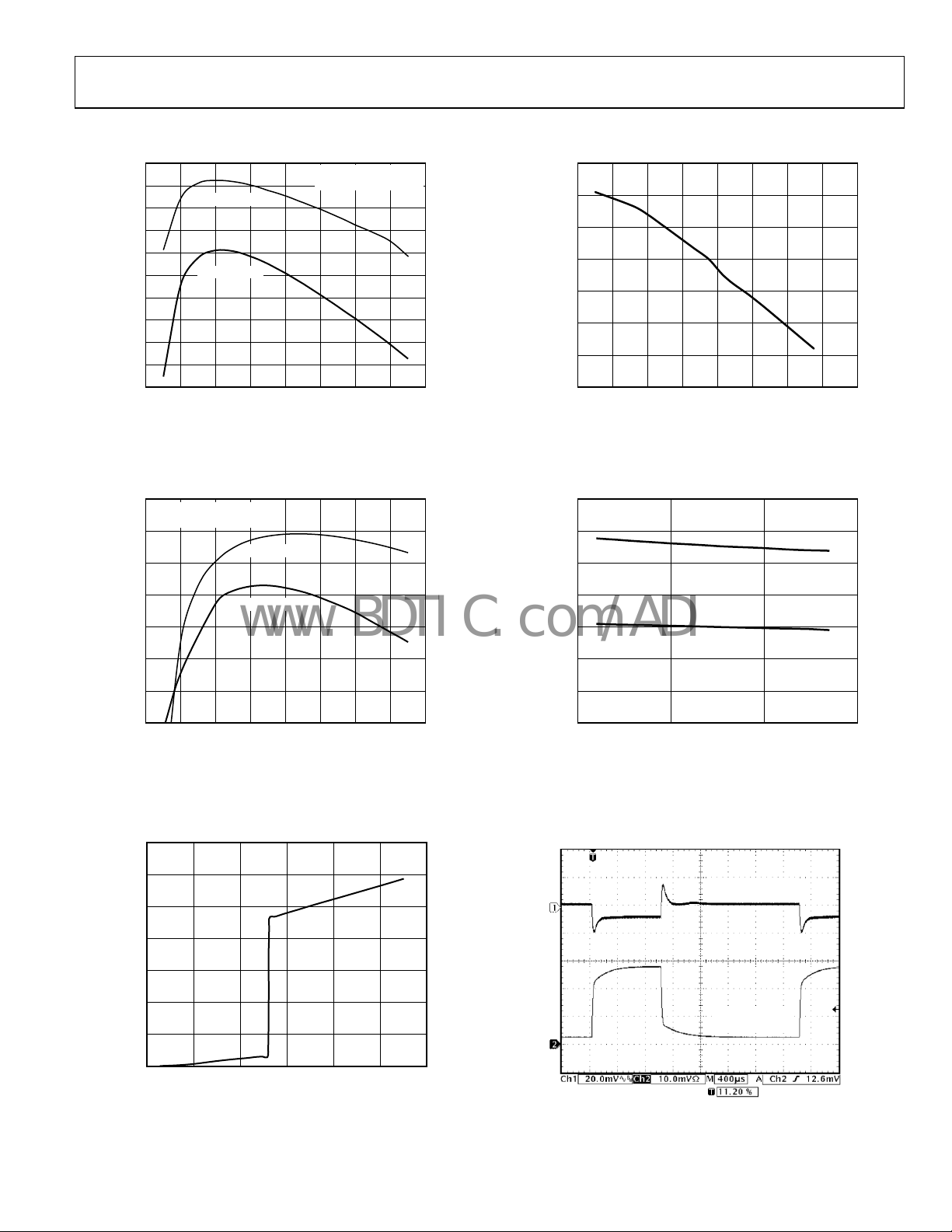
Figure 5. Efficiency vs. Load Current, V
94
TA = 25°C
FREQUENCY = 300kHz
92
90
88
86
EFFICIENCY (%)
84
82
80
0
2 4 6 8 10 12 14
3.3V OUTPUT
1.8V OUTPUT
LOAD CURRENT (A)
Figure 6. Efficiency vs. Load Current, V
1400
1200
1000
= 5 V, V
IN
= 12 V, V
IN
= 3.3 V, 1.8 V
OUT
= 3.3 V, 1.8 V
OUT
Figure 8. FB Regulation Voltage vs. Temperature
700
600
500
400
300
200
SWITCHING FREQUENCY ( kHz)
100
0
16
05310-006
–50
600kHz
300kHz
050
TEMPERATURE (° C)
100
05310-009
Figure 9. Switching Frequency vs. Temperature
OUTPUT VOLTAGE
(20mV/DIV)
800
600
VCC CURRENT (µA)
400
200
0
0
12345
VCC VOLTAG E (V)
6
05310-007
Figure 7. VCC Supply Current vs. VCC Voltage
Rev. C | Page 7 of 24
LOAD CURRENT
(5A/DIV)
Figure 10. Load Transient Response, 1.5 A to 15 A
5310-010

ADP1821
www.BDTIC.com/ADI
OUTPUT VOLTAGE
OUTPUT VOLTAGE
(50mV/DIV)
(1V/DIV)
SHDN (5V/DIV)
INPUT VOLTAGE
(5V/DIV)
Figure 11. Line Transient Response, 10 V to 16 V
OUTPUT VO LTAGE
(1V/DIV)
SHDN (5V/DIV)
PWGD (5V/DIV)
Figure 12. Power-On Response
PWGD (5V/DIV)
5310-011
5310-013
Figure 13. Power-On Response, Prebiased Output
OUTPUT VOL TAGE
(1V/DIV)
LOAD CURRENT
(10A/DIV)
5310-012
Figure 14. Output Short-Circui
t Response and Recovery
5310-014
Rev. C | Page 8 of 24
 Loading...