

50 mA, High Voltage,
V
www.BDTIC.com/ADI
FEATURES
Wide input voltage range: 4 V to 28 V
Maximum output current: 50 mA
Low light load current:
28 μA at 0 μA load
35 μA at 100 μA load
Low shutdown current: 0.7 μA
Low dropout voltage: 275 mV @ 50 mA load
Initial accuracy: ±0.5%
Accuracy over line, load, and temperature: ±2%
Stable with small 1μF ceramic output capacitor
Fixed 3.3 V and 5.0 V output voltage options
Adjustable output voltage option: 1.225 V to 5.0 V
Current limit and thermal overload protection
Logic controlled enable
Space-saving thermally enhanced MSOP package
APPLICATIONS
DC-to-DC post regulation
PCMCIA regulation
Keep-alive power in portable equipment
Industrial applications
Micropower Linear Regulator
ADP1720
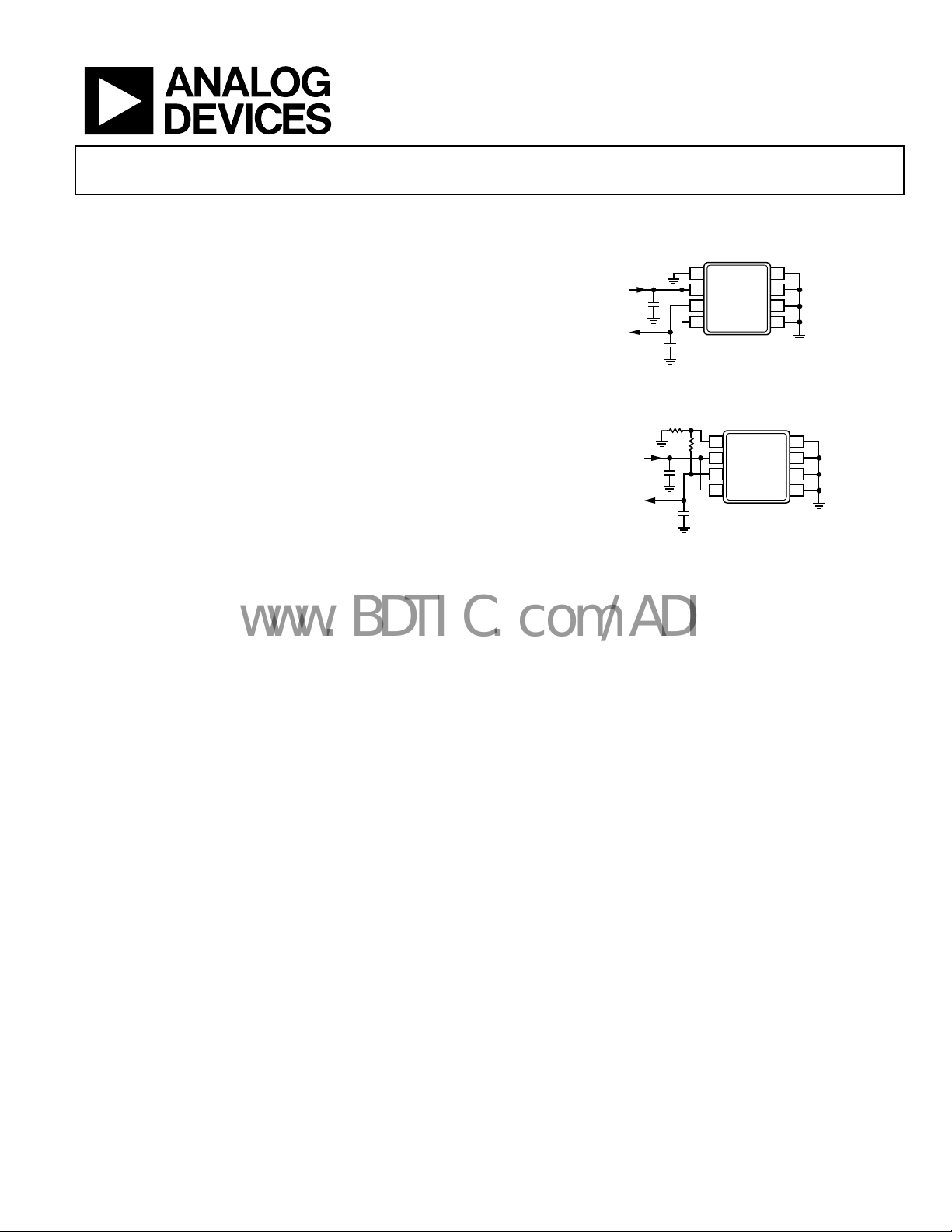
TYPICAL APPLICATION CIRCUITS
ADP1720
FIXED
1 8
VIN = 28V
1µF
= 5V
OUT
Figure 1. ADP1720 with Fixed Output Voltage, 5.0 V
1.225V(1 + R1/R2)
Figure 2. ADP1720 with Adjustable Output Voltage, 1.225 V to 5.0 V
VIN = 12V
V
OUT
1µF
1µF
=
2
3
4
R2
R1
1µF
GND
IN
OUT
EN
ADP1720
ADJUSTABLE
1
ADJ
2
IN
3
OUT
4
EN
GND
GND
GND
GND
GND
GND
GND
GND
7
6
5
06111-001
8
7
6
5
06111-002
GENERAL DESCRIPTION
The ADP1720 is a high voltage, micropower, low dropout linear
regulator. Operating over a very wide input voltage range of 4 V
to 28 V, the ADP1720 can provide up to 50 mA of output current.
With just 28 μA of quiescent supply current and a micropower
shutdown mode, this device is ideal for applications that require
low quiescent current.
The ADP1720 is available in fixed output voltages of 3.3 V and
5.0 V. An adjustable version is also available, which allows the
output to be set anywhere between 1.225 V and 5.0 V. An enable
function that allows external circuits to turn on and turn off the
ADP1720 output is available. For automatic startup, the enable
(EN) pin can be connected directly to the input rail.
The ADP1720 is optimized for stable operation with small 1 μF
ceramic output capacitors, allowing for good transient performance while occupying minimal board space.
The ADP1720 operates from –40°C to +125°C and uses current
limit protection and thermal overload protection circuits to
prevent damage to the device in adverse conditions.
Available in a small thermally enhanced MSOP package, the
ADP1720 provides a compact solution with low thermal resistance.
Rev. A
Information furnished by Analog Devices is believed to be accurate and reliable. However, no
responsibility is assumed by Analog Devices for its use, nor for any infringements of patents or other
rights of third parties that may result from its use. Specifications subject to change without notice. No
license is granted by implication or otherwise under any patent or patent rights of Analog Devices.
Trademarks and registered trademarks are the property of their respective owners.
One Technology Way, P.O. Box 9106, Norwood, MA 02062-9106, U.S.A.
Tel: 781.329.4700 www.analog.com
Fax: 781.461.3113 ©2007 Analog Devices, Inc. All rights reserved.

ADP1720
www.BDTIC.com/ADI
TABLE OF CONTENTS
Features .............................................................................................. 1
Applications ....................................................................................... 1
Typical Application Circuits ............................................................ 1
General Description ......................................................................... 1
Revision History ............................................................................... 2
Specifications ..................................................................................... 3
Absolute Maximum Ratings ............................................................ 5
Thermal Resistance ...................................................................... 5
ESD Caution .................................................................................. 5
Pin Configurations and Function Descriptions ........................... 6
REVISION HISTORY
7/07—Rev. 0 to Rev. A
Change to Figure 1 ........................................................................... 1
Changes to Table 1 ............................................................................ 3
Changes to Ordering Guide .......................................................... 15
2/07—Revision 0: Initial Version
Typical Performance Characteristics ..............................................7
Theory of Operation ...................................................................... 10
Adjustable Output Voltage (ADP1720 Adjustable) ............... 10
Applications Information .............................................................. 11
Capacitor Selection .................................................................... 11
Current Limit and Thermal Overload Protection ................. 11
Thermal Considerations ............................................................ 12
Printed Circuit Board Layout Considerations ....................... 14
Outline Dimensions ....................................................................... 15
Ordering Guide .......................................................................... 15
Rev. A | Page 2 of 16
ADP1720
V
V
www.BDTIC.com/ADI
SPECIFICATIONS
VIN = 12 V, I
Table 1.
Parameter Symbol Conditions Min Typ Max Unit
INPUT VOLTAGE RANGE VIN T
OPERATING SUPPLY CURRENT I
I
I
I
I
SHUTDOWN CURRENT I
EN = GND, TJ = –40°C to +125°C 1.5 μA
OUTPUT
Fixed Output V
Voltage Accuracy 100 μA < I
100 μA < I
Adjustable Output
Voltage Accuracy 100 μA < I
100 μA < I
Noise (10 Hz to 100 kHz)
REGULATION
Line Regulation ∆V
Load Regulation
1 mA < I
DROPOUT VOLTAGE
I
I
I
START-UP TIME
CURRENT LIMIT THRESHOLD
THERMAL CHARACTERISTICS
Thermal Shutdown
Threshold
Thermal Shutdown
Hysteresis
EN CHARACTERISTICS
EN Input
Logic High VIH 4 V ≤ VIN ≤ 28 V 1.8 V
Logic Low VIL 4 V ≤ VIN ≤ 28 V 0.4 V
Leakage Current V
EN = IN 0.5 1 μA
ADJ INPUT BIAS CURRENT
(ADP1720 ADJUSTABLE)
= 100 μA, CIN = C
OUT
1
V
2
3
V
4
T
5
I
= 1 μF, TA = 25°C, unless otherwise noted.
OUT
= –40°C to +125°C 4 28 V
J
I
GND
EN = GND 0.7 μA
GND-SD
I
OUT
I
OUT
NOISE
OUT
/∆VIN VIN = (V
OUT
∆V
/∆I
OUT
OUT
I
DROPOUT
200 μs
START-UP
55 90 140 mA
LIMIT
T
TS
SD
15
TS
SD-HYS
EN = GND 0.1 1 μA
I-LEAKAGE
ADJ
30 100 nA
I-BIAS
= 0 μA 28 μA
OUT
= 0 μA,
OUT
greater), T
= 100 μA 35 μA
OUT
= 100 μA, VIN = V
I
OUT
greater), T
= 1 mA 74 μA
OUT
= 1 mA, VIN = V
I
OUT
greater), T
= 10 mA 300 μA
OUT
= 10 mA, VIN = V
I
OUT
greater), T
100 μA < I
(whichever is greater), T
= 100 μA –0.5 +0.5 %
OUT
= 100 μA 1.2188 1.2250 1.2311 V
OUT
V
= 1.6 V, C
OUT
V
= 1.6 V, C
OUT
= 5 V, C
V
OUT
= 5 V, C
V
OUT
1 mA < I
= 10 mA 55 mV
OUT
= 10 mA, TJ = –40°C to +125°C 105 mV
OUT
= 50 mA 275 mV
OUT
= 50 mA, TJ = –40°C to +125°C 480 mV
OUT
rising 150
J
=
IN
= –40°C to +125°C
J
= –40°C to +125°C
J
= –40°C to +125°C
J
= –40°C to +125°C
J
< 50 mA, VIN = V
OUT
< 50 mA –1 +1 %
OUT
< 50 mA, TJ = –40°C to +125°C –2 +2 %
OUT
< 50 mA 1.2127 1.2372 V
OUT
< 50 mA, TJ = –40°C to +125°C 1.2005 1.2495 V
OUT
OUT
OUT
+ 0.5 V) to 28 V, TJ = –40°C to +125°C –0.02 +0.02 %/ V
OUT
< 50 mA 0.001 %/mA
OUT
< 50 mA, TJ = –40°C to +125°C 0.005 %/mA
OUT
+ 0.5 Vor 4V(whichever is
OUT
+ 0.5 V or 4 V (whichever is
OUT
+ 0.5 V or 4 V (whichever is
OUT
+ 0.5 V or 4 V (whichever is
OUT
+ 0.5 V or 4 V
OUT
= –40°C to +125°C
J
= 1 μF 146 μV rms
OUT
= 10 μF 124 μV rms
OUT
= 1 μF
= 10 μF
Rev. A | Page 3 of 16
80 μA
120 μA
340 μA
900 μA
1185 2115 μA
340 μV rms
266 μV rms
°C
°C

ADP1720
www.BDTIC.com/ADI
Parameter Symbol Conditions Min Typ Max Unit
POWER SUPPLY REJECTION RATIO PSRR f = 120 Hz, VIN = 8 V, V
f = 1 kHz, VIN = 8 V, V
f = 10 kHz, VIN = 8 V, V
f = 120 Hz, VIN = 8 V, V
f = 1 kHz, VIN = 8 V, V
f = 10 kHz, VIN = 8 V, V
1
Accuracy when OUT is connected directly to ADJ. When OUT voltage is set by external feedback resistors, absolute accuracy in adjust mode depends on the tolerances
of resistors used.
2
Based on an end-point calculation using 1 mA and 50 mA loads. See Fi for typical load regulation performance for loads less than 1 mA. gure 6
3
Dropout voltage is defined as the input to output voltage differential when the input voltage is set to the nominal output voltage. This applies only for output
voltages above 4 V.
4
Start-up time is defined as the time between the rising edge of EN to OUT being at 95% of its nominal value.
5
Current limit threshold is defined as the current at which the output voltage drops to 90% of the specified typical value. For example, the current limit for a 5.0 V
output voltage is defined as the current that causes the output voltage to drop to 90% of 5.0 V, or 4.5 V.
= 1.6 V –90 dB
OUT
= 1.6 V –80 dB
OUT
= 1.6 V –60 dB
OUT
= 5 V –83 dB
OUT
= 5 V –70 dB
OUT
= 5 V –50 dB
OUT
Rev. A | Page 4 of 16
ADP1720
www.BDTIC.com/ADI
ABSOLUTE MAXIMUM RATINGS
Table 2.
Parameter Rating
IN to GND –0.3 V to +30 V
OUT to GND
EN to GND –0.3 V to +30 V
ADJ to GND –0.3 V to +6 V
Storage Temperature Range –65°C to +150°C
Operating Junction
Temperature Range
Soldering Conditions JEDEC J-STD-020
Stresses above those listed under Absolute Maximum Ratings
may cause permanent damage to the device. This is a stress
rating only; functional operation of the device at these or any
other conditions above those indicated in the operational
section of this specification is not implied. Exposure to absolute
maximum rating conditions for extended periods may affect
device reliability.
–0.3 V to IN or +6 V
(whichever is less)
–40°C to +125°C
THERMAL RESISTANCE
θJA is specified for the worst-case conditions, that is, a device
soldered in a circuit board for surface-mount packages.
Table 3. Thermal Resistance
Package Type θJA θ
8-Lead MSOP 118 57 °C/W
Unit
JC
ESD CAUTION
Rev. A | Page 5 of 16

ADP1720
www.BDTIC.com/ADI
PIN CONFIGURATIONS AND FUNCTION DESCRIPTIONS
GND
OUT
IN
1
ADP1720
2
FIXED
3
TOP VIEW
(Not to S cale)
4
1
8
GND
7
GND
6
GND
5
GNDEN
06111-003
ADJ
OUT
IN
ADP1720
2
ADJUSTABLE
3
TOP VIEW
(Not to S cal e)
4
8
GND
7
GND
6
GND
5
GNDEN
Figure 3. 8-Lead MSOP Figure 4. 8-Lead MSOP
Table 4. Pin Function Descriptions
ADP1720
Fixed
Pin No.
ADP1720
Adjustable
Pin No. Mnemonic Description
1 N/A GND This pin is internally connected to ground.
N/A 1 ADJ Adjust. A resistor divider from OUT to ADJ sets the output voltage.
2 2 IN Regulator Input Supply. Bypass IN to GND with a 1 μF or greater capacitor.
3 3 OUT Regulated Output Voltage. Bypass OUT to GND with a 1 μF or greater capacitor.
4 4 EN
Enable Input. Drive EN high to turn on the regulator; drive it low to turn off the regulator. For
automatic startup, connect EN to IN.
5 5 GND Ground.
6 6 GND Ground.
7 7 GND Ground.
8 8 GND Ground.
06111-004
Rev. A | Page 6 of 16

ADP1720
www.BDTIC.com/ADI
TYPICAL PERFORMANCE CHARACTERISTICS
VIN = 12 V, V
5.03
OUT
= 5 V, I
= 100 μA, CIN = C
OUT
= 1 μF, TA = 25°C, unless otherwise noted.
OUT
1200
5.02
5.01
5.00
(V)
OUT
V
4.99
= 10µA
I
–40
LOAD
I
LOAD
I
LOAD
I
LOAD
I
LOAD
I
LOAD
= 100µA
= 1mA
= 10mA
= 25mA
= 50mA
–5 25 85 125
T
(°C)
J
111-005
06
4.98
4.97
4.96
Figure 5. Output Voltage vs. Junction Temperature
5.0015
5.0010
5.0005
5.0000
4.9995
(V)
4.9990
OUT
V
4.9985
4.9980
4.9975
4.9970
4.9965
0.01 100
0.1 1 10
(mA)
I
LOAD
111-006
06
Figure 6. Output Voltage vs. Load Current
(V)
OUT
V
5.010
5.008
5.006
5.004
5.002
5.000
4.998
4.996
4.994
4.992
4.990
I
= 10µA
LOAD
I
= 100µA
LOAD
I
= 1mA
LOAD
I
= 10mA
LOAD
I
= 25mA
LOAD
I
= 50mA
LOAD
03
5 10152025
V
(V)
IN
06111-007
0
Figure 7. Output Voltage vs. Input Voltage
1000
800
(µA)
600
GND
I
400
200
0
–40
Figure 8. Ground Current vs. Junction Temperature
1200
1000
800
(µA)
600
GND
I
400
200
0
0.01 100
Figure 9. Ground Current vs. Load Current
1400
1200
1000
800
(µA)
GND
600
I
400
200
0
03
Figure 10. Ground Current vs. Input Voltage
I
= 50mA
LOAD
I
= 25mA
LOAD
I
= 10mA
LOAD
–5 25 85 125
0.1 1 10
I
LOAD
I
LOAD
I
LOAD
I
LOAD
5 10152025
T
(°C)
J
= 50mA
= 25mA
= 10mA
V
IN
(mA)
(V)
I
LOAD
I
LOAD
I
LOAD
= 1mA
= 100µA
= 10µA
I
LOAD
I
LOAD
I
LOAD
= 1mA
= 100µA
= 10µA
06111-008
06111-009
06111-010
0
Rev. A | Page 7 of 16

ADP1720
www.BDTIC.com/ADI
300
250
200
(mV)
150
DROPOUT
V
100
50
0
11
I
LOAD
10
(mA)
06111-011
00
Figure 11. Dropout Voltage vs. Load Current
5.05
I
= 1mA
LOAD
5.00
4.95
4.90
4.85
(V)
OUT
4.80
V
4.75
4.70
4.65
4.60
4.9 5.4
5.0 5.1 5.2 5.3
I
LOAD
I
LOAD
I
LOAD
= 10mA
V
(V)
IN
= 50mA
= 25mA
06111-012
Figure 12. Output Voltage vs. Input Voltage (in Dropout)
3.5
3.0
2.5
2.0
(mA)
GND
1.5
I
I
1.0
I
=
LOAD
0.5
1mA
0
4.9 5.4
5.0 5.1 5.2 5.3
LOAD
10mA
I
LOAD
25mA
=
V
(V)
IN
I
LOAD
50mA
=
Figure 13. Ground Current vs. Input Voltage (in Dropout)
0
VIN = 8V
= 1.6V
V
–10
OUT
= 1µF
C
OUT
V
–20
–30
–40
–50
PSRR (dB)
–60
–70
–80
–90
–100
10 10M
= 50mV
RIPPLE
100µA
100 1k 10k 100k 1M
FREQUENCY (Hz)
1mA
10mA
Figure 14. Power Supply Rejection Ratio vs. Frequency
=
06111-013
06111-014
(1.6 V Adjustable Output)
Rev. A | Page 8 of 16

ADP1720
V
V
V
V
V
www.BDTIC.com/ADI
0
VIN = 8V
= 5V
V
–10
OUT
C
= 1µF
OUT
= 50mV
V
–20
RIPPLE
–30
–40
–50
PSRR (dB)
–60
–70
–80
–90
–100
10 10M
100 1k 10k 100k 1M
FREQUENCY (Hz)
100µA
1mA
10mA
Figure 15. Power Supply Rejection Ratio vs. Frequency
(5.0 V Fixed Output)
VIN = 12V
V
= 1.6V
OUT
C
= 1µF
IN
C
= 1µF
OUT
LOAD STE P FROM 2. 5mA TO 47.5mA
1
2V/DI
2
10mV/DI
06111-015
1
5V/DI
VIN STEP FROM 6V TO 7V
V
= 5V
OUT
C
= 1µF
IN
C
= 1µF
OUT
I
= 50mA
LOAD
V
OUT
TIME (100µs/DIV)
Figure 17. Line Transient Response
EN
06111-017
V
1
10mV/DI
OUT
TIME (20µs/DIV)
Figure 16. Load Transient Response
V
OUT
VIN = 12V
V
= 5V
OUT
C
= 1µF
2
06111-016
2V/DI
TIME (40µs/DIV)
IN
C
OUT
I
LOAD
= 1µF
= 50mA
06111-018
Figure 18. Start-Up Time
Rev. A | Page 9 of 16

ADP1720
www.BDTIC.com/ADI
THEORY OF OPERATION
The ADP1720 is a low dropout, BiCDMOS linear regulator that
operates from a 4 V to 28 V input rail and provides up to 50 mA
of output current. Ground current in shutdown mode is typically
700 nA. The ADP1720 is stable and provides high power supply
rejection ratio (PSRR) and excellent line and load transient
response with just a small 1 μF ceramic output capacitor.
IN
CURRENT LIMIT
THERMAL PROTECT
SHUTDOWN
EN
REFERENCE
GND
Figure 19. Internal Block Diagram
Internally, the ADP1720 consists of a reference, an error amplifier, a feedback voltage divider, and a DMOS pass transistor.
Output current is delivered via the DMOS pass device, which is
controlled by the error amplifier. The error amplifier compares
the reference voltage with the feedback voltage from the output
and amplifies the difference. If the feedback voltage is lower than
the reference voltage, the gate of the DMOS device is pulled
lower, allowing more current to pass and increasing the output
voltage. If the feedback voltage is higher than the reference
voltage, the gate of the PNP device is pulled higher, allowing
less current to pass and decreasing the output voltage.
The ADP1720 is available in two versions, one with fixed output
voltage options (see Figure 1) and one with an adjustable output
voltage (see Figure 2). The fixed output voltage options are set
internally to either 5.0 V or 3.3 V, using an internal feedback
network. The adjustable output voltage can be set to between
1.225 V and 5.0 V by an external voltage divider connected from
OUT to ADJ. The ADP1720 uses the EN pin to enable and
disable the OUT pin under normal operating conditions. When
EN is high, OUT turns on; when EN is low, OUT turns off. For
automatic startup, EN can be tied to IN.
OUT
GND/ADJ
19
06111-0
ADJUSTABLE OUTPUT VOLTAGE (ADP1720 ADJUSTABLE)
The ADP1720 adjustable version can have its output voltage
set over a 1.225 V to 5.0 V range. The output voltage is set by
connecting a resistive voltage divider from OUT to ADJ. The
output voltage is calculated using the equation
V
= 1.225 V (1 + R1/R2) (1)
OUT
where:
R1 is the resistor from OUT to ADJ.
R2 is the resistor from ADJ to GND.
To make calculation of R1 and R2 easier, Equation 1 can be
rearranged as follows:
R1 = R2 [(V
The maximum bias current into ADJ is 100 nA; therefore,
when less than 0.5% error is due to the bias current, use values
less than 60 kΩ for R2.
/1.225) – 1] (2)
OUT
Rev. A | Page 10 of 16

ADP1720
V
V
www.BDTIC.com/ADI
APPLICATIONS INFORMATION
CAPACITOR SELECTION
Output Capacitor
The ADP1720 is designed for operation with small, space-saving
ceramic capacitors, but it functionswith most commonly used
capacitors as long as care is taken about the effective series
resistance (ESR) value. The ESR of the output capacitor affects
stability of the LDO control loop. A minimum of 1 μF capacitance
with an ESR of 500 mΩ or less is recommended to ensure stability of the ADP1720. Transient response to changes in load
current is also affected by output capacitance. Using a larger
value of output capacitance improves the transient response of
the ADP1720 to large changes in load current. Figure 20 and
Figure 21 show the transient responses for output capacitance
values of 1 μF and 10 μF, respectively.
Input and Output Capacitor Properties
Any good quality ceramic capacitors can be used with the
ADP1720, as long as they meet the minimum capacitance and
maximum ESR requirements. Ceramic capacitors are manufactured with a variety of dielectrics, each with different behavior
over temperature and applied voltage. Capacitors must have a
dielectric adequate to ensure the minimum capacitance over
the necessary temperature range and dc bias conditions. X5R
or X7R dielectrics with a voltage rating of 6.3 V or 10 V are
recommended for the output capacitor. X5R or X7R dielectrics
with a voltage rating of 50 V or higher are recommended for the
input capacitor.
Y5V and Z5U dielectrics are not recommended, due to their
poor temperature and dc bias characteristics.
VIN = 12V
V
= 1.6V
OUT
C
= 1µF
IN
C
= 1µF
OUT
LOAD STEP FROM 2. 5 mA T O 47.5mA
1
10mV/DI
TIME (2µs/DIV)
Figure 20. Output Transient Response, 1 μF
VIN = 12V
V
= 1.6V
OUT
C
= 10µF
IN
C
= 10µF
OUT
LOAD STEP FROM 2. 5mA TO 47.5mA
1
10mV/DI
TIME (2µs/DIV)
Figure 21. Output Transient Response, 10 μF
06111-020
1-0210611
Input Bypass Capacitor
Connecting a 1 μF capacitor from IN to GND reduces the circuit sensitivity to printed circuit board (PCB) layout, especially
when encountering long input traces or high source impedance.
If greater than 1 μF of output capacitance is required, it is
recommended that the input capacitor be increased to match it.
CURRENT LIMIT AND THERMAL OVERLOAD PROTECTION
Current limit and thermal overload protection circuits on the
ADP1720 protect the part from damage caused by excessive power
dissipation. The ADP1720 is designed to current limit when
the output load reaches 90 mA (typical). When the output
load exceeds 90 mA, the output voltage is reduced to maintain
a constant current limit.
Thermal overload protection is included, which limits the junction
temperature to a maximum of 150°C (typical). Under extreme
conditions (that is, high ambient temperature and power dissipation), when the junction temperature starts to rise above 150°C,
the output is turned off, reducing the output current to zero.
When the junction temperature drops below 135°C, the output is
turned on again, and output current is restored to its nominal value.
Consider the case where a hard short from OUT to GND occurs.
At first, the ADP1720 current limits so that only 90 mA is
conducted into the short. If self-heating of the junction is
great enough to cause its temperature to rise above 150°C,
thermal shutdown activates, turning off the output and
reducing the output current to zero. As the junction
temperature cools and drops below 135°C, the output turns on
and conducts 90 mA into the short, again causing the junction
temperature to rise above 150°C. This thermal oscillation
between 135°C and 150°C causes a current oscillation between
90 mA and 0 mA, which continues as long as the short
remains at the output.
Current and thermal limit protections are intended to protect
the device against accidental overload conditions. For reliable
operation, device power dissipation must be externally limited
so that junction temperatures do not exceed 125°C.
Rev. A | Page 11 of 16

ADP1720
www.BDTIC.com/ADI
THERMAL CONSIDERATIONS
To guarantee reliable operation, the junction temperature of the
ADP1720 must not exceed 125°C. To ensure the junction temperature stays below this maximum value, the user needs to be
aware of the parameters that contribute to junction temperature
changes. These parameters include ambient temperature, power
dissipation in the power device, and thermal resistances between
the junction and ambient air (θ
on the package assembly compounds used and the amount of
copper to which the GND pins of the package are soldered on the
PCB. Tabl e 5 shows typical θ
for various PCB copper sizes.
Table 5.
Copper Size (mm2)
01 118
50 99
100 77
300 75
500 74
1
Device soldered to minimum size pin traces.
The junction temperature of the ADP1720 can be calculated
from the following equation:
T
= TA + (PD × θJA) (3)
J
where:
T
is the ambient temperature.
A
is the power dissipation in the die, given by
P
D
P
= [(VIN – V
D
OUT
) × I
where:
I
is the load current.
LOAD
is the ground current.
I
GND
V
and V
IN
are input and output voltages, respectively.
OUT
Power dissipation due to ground current is quite small and
can be ignored. Therefore, the junction temperature equation
simplifies to the following:
T
= TA + {[(VIN – V
J
As shown in Equation 5, for a given ambient temperature,
input-to-output voltage differential, and continuous load
current, there exists a minimum copper size requirement for
the PCB to ensure that the junction temperature does not rise
above 125°C. Figure 22 to Figure 27 show junction temperature
calculations for different ambient temperatures, load currents,
V
IN
to V
differentials, and areas of PCB copper.
OUT
). The θJA number is dependent
JA
values of the 8-lead MSOP package
JA
θ
(°C/W)
JA
LOAD
OUT
] + (VIN × I
) × I
LOAD
] × θJA} (5)
) (4)
GND
140
120
100
80
(°C)
J
T
60
40
20
0
028
140
120
100
80
(°C)
J
T
60
40
20
0
02
140
120
100
80
(°C)T
J
60
40
20
0
02
MAX TJ (DO NOT OPE RAT E ABOVE THIS P O INT)
1mA
5mA
4 8 12 16 20 24
10mA
20mA
30mA
40mA
V
– V
(V)
IN
OUT
50mA
(LOAD CURRENT)
Figure 22. 300 mm2 of PCB Copper, TA = 25°C
MAX TJ (DO NOT OPE RAT E ABOVE THIS P O INT)
1mA
5mA
4 8 12 16 20 24
10mA
20mA
30mA
40mA
V
– V
(V)
IN
OUT
50mA
(LOAD CURRENT)
Figure 23. 100 mm2 of PCB Copper, TA = 25°C
MAX TJ (DO NOT OPE RAT E ABOVE THIS P O INT)
1mA
5mA
4 8 12 16 20 24
10mA
20mA
30mA
40mA
V
– V
(V)
IN
OUT
50mA
(LOAD CURRENT)
Figure 24. 0 mm2 of PCB Copper, TA = 25°C
06111-022
06111-023
8
1-0240611
8
Rev. A | Page 12 of 16

ADP1720
www.BDTIC.com/ADI
140
MAX TJ (DO NOT OPE RAT E ABOVE THIS P O INT)
120
140
MAX TJ (DO NOT OPE RAT E ABOVE THIS P O INT)
120
100
80
(°C)
J
T
60
40
20
1mA
5mA
0
4 8 12 16 20 24
02
10mA
20mA
30mA
40mA
V
– V
(V)
IN
OUT
50mA
(LOAD CURRENT)
111-02506
8
Figure 25. 300 mm2 of PCB Copper, TA = 50°C
140
MAX TJ (DO NOT OPE RAT E ABOVE THIS P O INT)
120
100
80
(°C)
J
T
60
40
20
1mA
5mA
0
4 8 12 16 20 24
028
10mA
20mA
30mA
40mA
V
– V
(V)
IN
OUT
50mA
(LOAD CURRENT)
06111-026
100
80
(°C)
J
T
60
40
20
1mA
5mA
0
4 8 12 16 20 24
02
Figure 27. 0 mm2 of PCB Copper, TA = 50°C
Figure 26. 100 mm2 of PCB Copper, TA = 50°C
10mA
20mA
30mA
40mA
V
– V
(V)
IN
OUT
50mA
(LOAD CURRENT)
06111-027
8
Rev. A | Page 13 of 16

ADP1720
www.BDTIC.com/ADI
PRINTED CIRCUIT BOARD LAYOUT CONSIDERATIONS
Heat dissipation from the package can be improved by increasing
the amount of copper attached to the pins of the ADP1720. However, as can be seen from Ta b le 5, a point of diminishing returns
eventually is reached, beyond which an increase in the copper
size does not yield significant heat dissipation benefits.
Place the input capacitor as close as possible to the IN and GND
pins. Place the output capacitor as close as possible to the OUT
and GND pins. Use of 0402 or 0603 size capacitors and resistors
achieves the smallest possible footprint solution on boards
where area is limited.
GND (TOP)
ADP1720
IN OUT
R2
GND (BOTTOM)
Figure 28. Example PCB Layout
C2C1
R1
EN
06111-028
Rev. A | Page 14 of 16

ADP1720
www.BDTIC.com/ADI
OUTLINE DIMENSIONS
3.20
3.00
2.80
8
5
3.20
3.00
1
2.80
PIN 1
0.65 BSC
0.95
0.85
0.75
0.15
0.38
0.00
0.22
COPLANARITY
0.10
COMPLIANT TO JEDEC STANDARDS MO-187-AA
Figure 29. 8-Lead Mini Small Outline Package [MSOP]
ORDERING GUIDE
Model Temperature Range
ADP1720ARMZ-5-R7
ADP1720ARMZ-3.3-R7
ADP1720ARMZ-R7
ADP1720-5-EVALZ
ADP1720-3.3-EVALZ
ADP1720-EVALZ
1
Z = RoHS Compliant Part.
1
–40°C to +125°C 5 8-Lead MSOP RM-8 L30
1
–40°C to +125°C 3.3 8-Lead MSOP RM-8 L2Z
1
–40°C to +125°C 1.225 to 5 8-Lead MSOP RM-8 L2M
1
5 Evaluation Board
1
3.3 Evaluation Board
1
1.225 to 5 Evaluation Board
5.15
4.90
4.65
4
1.10 MAX
0.23
SEATING
PLANE
0.08
(RM-8)
Dimensions shown in millimeters
Output
Voltage (V)
8°
0°
0.80
0.60
0.40
Package Description Package Option Branding
Rev. A | Page 15 of 16

ADP1720
www.BDTIC.com/ADI
NOTES
©2007 Analog Devices, Inc. All rights reserved. Trademarks and
registered trademarks are the property of their respective owners.
D06111-0-7/07(A)
Rev. A | Page 16 of 16
 Loading...