

500 mA, Low Dropout,
V
V
A
FEATURES
Maximum output current: 500 mA
Input voltage range: 2.5 V to 5.5 V
Low shutdown current: <1 μA
Low dropout voltage:
250 mV @ 500 mA load
50 mV @ 100 mA load
Initial accuracy: ±1%
Accuracy over line, load, and temperature: ±3%
16 fixed output voltage options with soft start:
0.75 V to 3.3 V (ADP1715)
Adjustable output voltage option: 0.8 V to 5.0 V
(ADP1715 Adjustable)
16 fixed output voltage options with tracking:
0.75 V to 3.3 V (ADP1716)
Stable with small 2.2 μF ceramic output capacitor
Excellent load/line transient response
Current limit and thermal overload protection
Logic controlled enable
8-lead thermally enhanced MSOP package
APPLICATIONS
Notebook computers
Memory components
Telecommunications equipment
Network equipment
DSP/FPGA/μP supplies
Instrumentation equipment/data acquisition systems
CMOS Linear Regulator
ADP1715/ADP1716
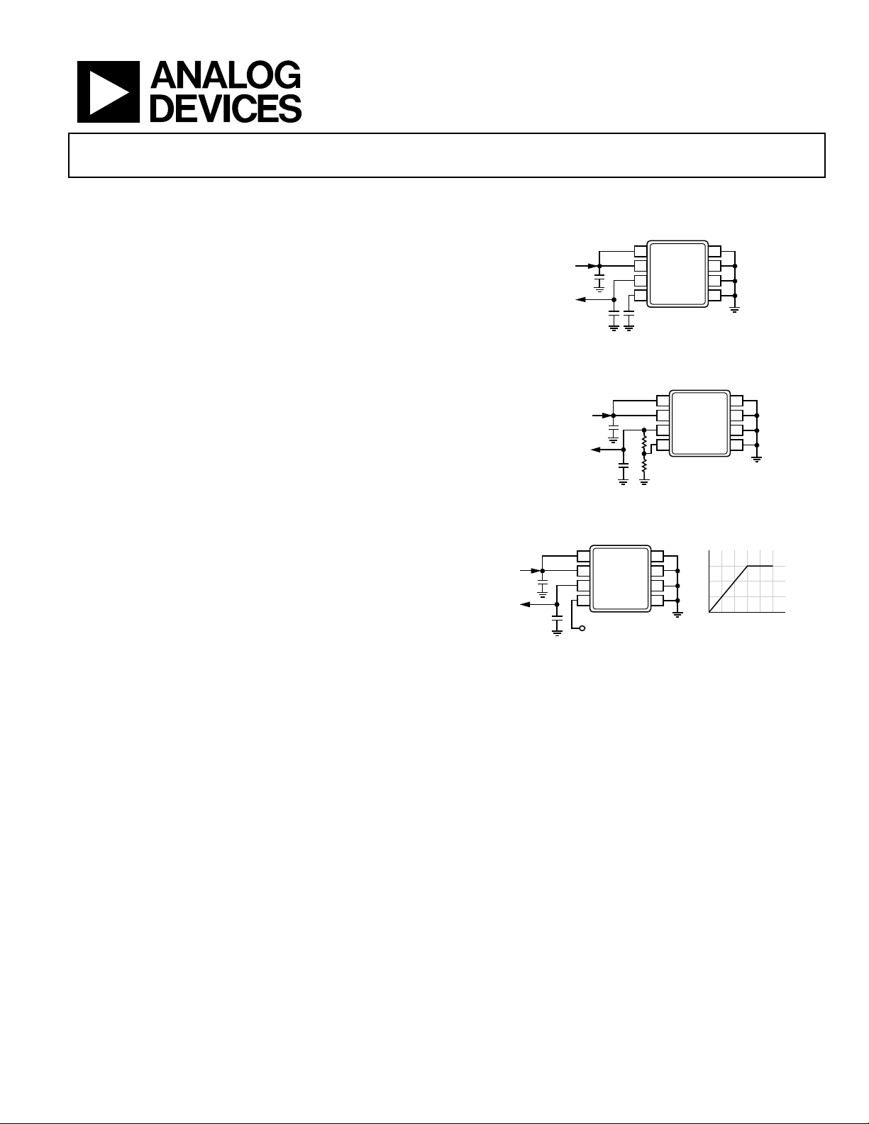
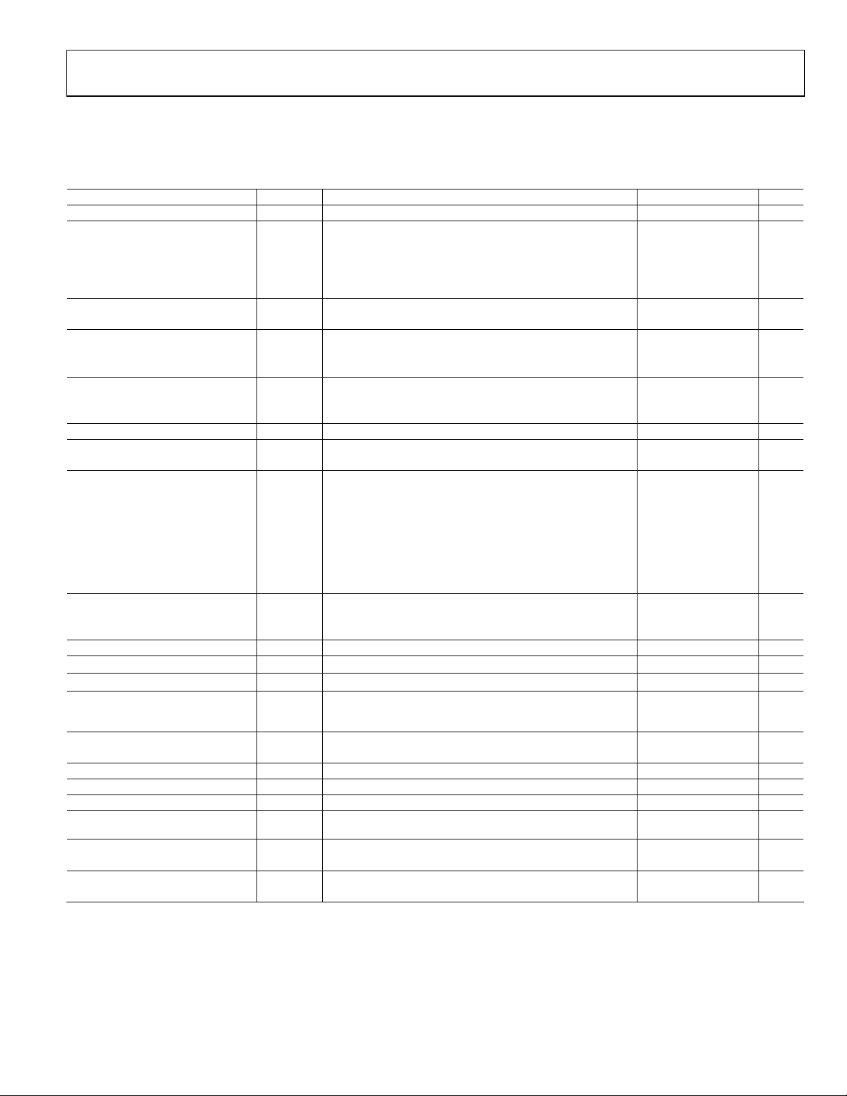
TYPICAL APPLICATION CIRCUITS
ADP1715
1
EN
VIN = 5V
OUT
2.2µF
= 3.3V
2
IN
3
OUT
4
SS
10nF2.2µF
Figure 1. ADP1715 with Fixed Output Voltage, 3.3 V
1
2
3
R1
4
R2
= 0.8(1 + R1/R2)
OUT
VIN = 5V
2.2µF
2.2µF
Figure 2. ADP1715 with Adjustable Output Voltage, 0.8 V to 5.0 V
DP1716
VIN = 5V
V
OUT
2.2µF
2.2µF
1
2
3
4
V
EN
IN
OUT
TRK
= 0V TO 5V
TRK
GND
GND
GND
GND
8
7
6
5
Figure 3. ADP1716 with Output Voltage Tracking
8
GND
7
GND
6
GND
5
GND
ADP1715
ADJUSTABLE
GND
EN
IN
GND
OUT
GND
ADJ
GND
V
(V)
OUT
3
2
1
0
8
7
6
5
12345
V
TRK
(V)
06110-001
06110-002
06110-003
GENERAL DESCRIPTION
The ADP1715/ADP1716 are low dropout, CMOS linear
regulators that operate from 2.5 V to 5.5 V and provide up to
500 mA of output current. Using an advanced proprietary
architecture, they provide high power supply rejection and
achieve excellent line and load transient response with just a
small 2.2 μF ceramic output capacitor.
Three versions of this part are available, one with fixed
output voltage options and variable soft start (ADP1715),
one with adjustable output voltage and fixed soft start
(ADP1715 Adjustable), and one with voltage tracking in
fixed output voltage options (ADP1716). The fixed output
voltage options are internally set to one of sixteen values
Rev. 0
Information furnished by Analog Devices is believed to be accurate and reliable. However, no
responsibility is assumed by Anal og Devices for its use, nor for any infringements of patents or ot her
rights of third parties that may result from its use. Specifications subject to change without notice. No
license is granted by implication or otherwise under any patent or patent rights of Analog Devices.
Trademarks and registered trademarks are the property of their respective owners.
between 0.75 V and 3.3 V; the adjustable output voltage can
be set to any value between 0.8 V and 5.0 V by an external
voltage divider connected from OUT to ADJ. The variable
soft start uses an external capacitor at SS to control the
output voltage ramp. Tracking limits the output voltage to
the at-or-below voltage at the TRK pin.
The ADP1715/ADP1716 are available in 8-lead thermally
enhanced MSOP packages, making them not only a very
compact solution but also providing excellent thermal
performance for applications requiring up to 500 mA of output
current in a small, low profile footprint.
One Technology Way, P.O. Box 9106, Norwood, MA 02062-9106, U.S.A.
Tel: 781.329.4700 www.analog.com
Fax: 781.461.3113 ©2006 Analog Devices, Inc. All rights reserved.

ADP1715/ADP1716
TABLE OF CONTENTS
Features.............................................................................................. 1
Track Mode (ADP1716)............................................................ 11
Applications....................................................................................... 1
Typical Application Circuits............................................................ 1
General Description ......................................................................... 1
Revision History ............................................................................... 2
Specifications..................................................................................... 3
Absolute Maximum Ratings............................................................ 4
Thermal Resistance ...................................................................... 4
ESD Caution.................................................................................. 4
Pin Configurations and Function Descriptions ........................... 5
Typical Performance Characteristics ............................................. 6
Theory of Operation ...................................................................... 10
Soft-Start Function (ADP1715)................................................ 10
Adjustable Output Voltage (ADP1715 Adjustable) ...............11
REVISION HISTORY
Enable Feature ............................................................................ 11
Application Information................................................................ 12
Capacitor Selection .................................................................... 12
Current Limit and Thermal Overload Protection ................. 12
Thermal Considerations............................................................ 12
Printed Circuit Board Layout Considerations ....................... 15
Outline Dimensions....................................................................... 16
Ordering Guide .......................................................................... 17
9/06—Rev. 0: Initial Version
Rev. 0 | Page 2 of 20
ADP1715/ADP1716
SPECIFICATIONS
VIN = (V
+ 0.5 V) or 2.5 V (whichever is greater), I
OUT
= 10 mA, CIN = C
OUT
= 2.2 μF, TA = 25°C, unless otherwise noted.
OUT
Table 1.
Parameter Symbol Conditions Min Typ Max Unit
INPUT VOLTAGE RANGE VIN T
OPERATING SUPPLY CURRENT I
I
GND
I
I
I
100 μA < I
SHUTDOWN CURRENT I
EN = GND 0.1 μA
GND-SD
EN = GND, TJ = –40°C to +125°C 1.0 μA
FIXED OUTPUT VOLTAGE ACCURACY V
I
OUT
(ADP1715 and ADP1716 ONLY) I
100 μA < I
ADJUSTABLE OUTPUT VOLTAGE V
I
OUT
ACCURACY (ADP1715 ADJUSTABLE)1 I
100 μA < I
LINE REGULATION ∆V
LOAD REGULATION
2
/∆VIN VIN = (V
OUT
∆V
/∆I
OUT
I
DROPOUT VOLTAGE
3
V
DROPOUT
I
I
I
I
I
I
I
START-UP TIME
4
T
START-UP
ADP1715 Adjustable and ADP1716 100 μs
ADP1715 with External Soft Start CSS = 10 nF 7.3 ms
CURRENT LIMIT THRESHOLD
5
I
550 750 1200 mA
LIMIT
THERMAL SHUTDOWN THRESHOLD TSSD T
THERMAL SHUTDOWN HYSTERESIS TS
SOFT-START SOURCE CURRENT
SS
SD-HYS
I-SOURCE
(ADP1715 WITH EXTERNAL
SOFT START)
V
to V
OUT
ACCURACY V
TRK
TRK-ERROR
(ADP1716) 0 V ≤ V
EN INPUT LOGIC HIGH VIH 2.5 V ≤ VIN ≤ 5.5 V 1.8 V
EN INPUT LOGIC LOW VIL 2.5 V ≤ VIN ≤ 5.5 V 0.4 V
EN INPUT LEAKAGE CURRENT V
ADJ INPUT BIAS CURRENT
I-LEAKAGE
ADJ
I-BIAS
(ADP1715 ADJUSTABLE)
OUTPUT NOISE OUT
NOISE
10 Hz to 100 kHz, V
POWER SUPPLY REJECTION RATIO PSRR 1 kHz, V
1 kHz, V
1
Accuracy when OUT is connected directly to ADJ. When OUT voltage is set by external feedback resistors, absolute accuracy in adjust mode depends on the tolerances
of resistors used.
2
Based on an end-point calculation using 10 mA and 500 mA loads. See Figure 8 for typical load regulation performance for loads less than 10 mA.
3
Dropout voltage is defined as the input to output voltage differential when the input voltage is set to the nominal output voltage. This applies only for output
voltages above 2.5 V.
4
Start-up time is defined as the time between the rising edge of EN to OUT being at 95% of its nominal value.
5
Current limit threshold is defined as the current at which the output voltage drops to 90% of the specified typical value. For example, the current limit for a 1.0 V
output voltage is defined as the current that causes the output voltage to drop to 90% of 1.0 V, or 0.9 V.
= –40°C to +125°C 2.5 5.5 V
J
= 100 μA 65 μA
OUT
= 100 μA, TJ = –40°C to +125°C 100 μA
OUT
= 100 mA 160 μA
OUT
= 100 mA, TJ = –40°C to +125°C 220 μA
OUT
< 500 mA, TJ = –40°C to +125°C 650 μA
OUT
= 10 mA –1 +1 %
OUT
= 10 mA to 500 mA –2 +2 %
OUT
< 500 mA, TJ = –40°C to +125°C –3 +3 %
OUT
= 10 mA 0.792 0.8 0.808 V
OUT
= 10 mA to 500 mA 0.784 0.816 V
OUT
< 500 mA, TJ = –40°C to +125°C 0.776 0.824 V
OUT
+ 0.5 V) to 5.5 V, TJ = –40°C to +125°C –0.15 +0.15 %/ V
OUT
I
OUT
I
= 10 mA to 500 mA 0.002 %/mA
OUT
= 10 mA to 500 mA, TJ = –40°C to +125°C 0.004 %/mA
OUT
= 100 mA, V
OUT
= 100 mA, V
OUT
= 500 mA, V
OUT
= 500 mA, V
OUT
= 100 mA, 2.5 V ≤ V
OUT
= 100 mA, 2.5 V ≤ V
OUT
= 500 mA, 2.5 V ≤ V
OUT
= 500 mA, 2.5 V ≤ V
OUT
≥ 3.3 V 50 mV
OUT
≥ 3.3 V, TJ = –40°C to +125°C 100 mV
OUT
≥ 3.3 V 250 300 mV
OUT
≥ 3.3 V, TJ = –40°C to +125°C 400 mV
OUT
< 3.3 V 60 mV
OUT
< 3.3 V, TJ = –40°C to +125°C 100 mV
OUT
< 3.3 V 320 400 mV
OUT
< 3.3 V, TJ = –40°C to +125°C 500 mV
OUT
rising 150
J
15
°C
°C
SS = GND 0.7 1.2 1.7 μA
0 V ≤ V
≤ (0.5 × V
TRK
≤ (0.5 × V
TRK
OUT(NOM)
OUT(NOM)
), V
), V
≤ 1.8 V, TJ = –40°C to +125°C –50 +50 mV
OUT(NOM)
> 1.8 V, TJ = –40°C to +125°C –100 +100 mV
OUT(NOM)
EN = IN or GND 0.1 1 μA
30 100 nA
10 Hz to 100 kHz, V
= 0.75 V 67 dB
OUT
= 3.3 V 53 dB
OUT
= 0.75 V 125 μVrms
OUT
= 3.3 V 450 μVrms
OUT
Rev. 0 | Page 3 of 20
ADP1715/ADP1716
ABSOLUTE MAXIMUM RATINGS
Table 2.
Parameter Rating
IN to GND –0.3 V to +6 V
OUT to GND –0.3 V to IN
EN to GND –0.3 V to +6 V
SS/ADJ/TRK to GND –0.3 V to +6 V
Storage Temperature Range –65°C to +150°C
Operating Junction Temperature Range –40°C to +125°C
Soldering Conditions JEDEC J-STD-020
Stresses above those listed under Absolute Maximum Ratings
may cause permanent damage to the device. This is a stress
rating only; functional operation of the device at these or any
other conditions above those indicated in the operational
section of this specification is not implied. Exposure to absolute
maximum rating conditions for extended periods may affect
device reliability.
THERMAL RESISTANCE
θJA is specified for the worst-case conditions, that is, a device
soldered in a circuit board for surface-mount packages.
Table 3. Thermal Resistance
Package Type θJA Unit
8-Lead MSOP 118 °C/W
ESD CAUTION
Rev. 0 | Page 4 of 20
ADP1715/ADP1716
PIN CONFIGURATIONS AND FUNCTION DESCRIPTIONS
1
EN
ADP1715
2
IN
OUT
SS
FIXED
3
TOP VIEW
(Not to Scale)
4
Figure 4. 8-Lead MSOP (RM-Suffix) Figure 5. 8-Lead MSOP (RM-Suffix) Figure 6. 8-Lead MSOP (RM-Suffix)
Table 4. Pin Function Descriptions
ADP1715
Fixed
Pin No.
ADP1715
Adjustable
Pin No.
1 1 1 EN
2 2 2 IN Regulator Input Supply. Bypass IN to GND with a 2.2 μF or greater capacitor.
3 3 3 OUT
4 SS Soft Start. A capacitor connected to this pin determines the soft-start time.
4 ADJ Adjust. A resistor divider from OUT to ADJ sets the output voltage.
4 TRK
5, 6, 7, 8 5, 6, 7, 8 5, 6, 7, 8 GND Ground.
8
GND
7
GND
6
GND
5
GND
6110-004
EN
IN
OUT
ADJ
ADP1716
Pin No. Mnemonic Description
1
ADP1715
2
ADJUSTABLE
3
TOP VIEW
(Not to Scale)
4
8
GND
7
GND
6
GND
5
GND
6110-005
EN
OUT
TRK
IN
1
2
ADP1716
3
TOP VIEW
(Not to Scale)
4
8
GND
7
GND
6
GND
5
GND
6110-006
Enable Input. Drive EN high to turn on the regulator; drive it low to turn off the
regulator. For automatic startup, connect EN to IN.
Regulated Output Voltage. Bypass OUT to GND with a 2.2 μF or greater
capacitor.
Track. The output will follow the voltage placed on the TRK pin. (See the
Theory of Operation section for a more detailed description.)
Rev. 0 | Page 5 of 20
ADP1715/ADP1716
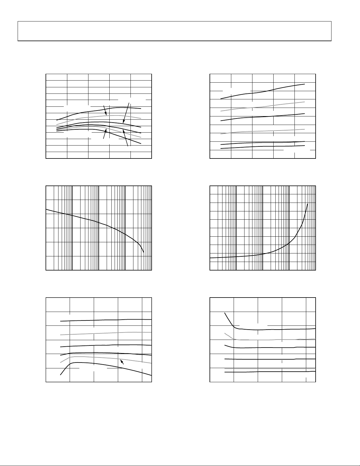
TYPICAL PERFORMANCE CHARACTERISTICS
VIN = 3.8 V, I
3.364
3.354
3.344
3.334
3.324
3.314
3.304
(V)
3.294
OUT
V
3.284
3.274
3.264
3.254
3.244
3.234
Figure 7. Output Voltage vs. Junction Temperature
3.325
3.315
3.305
(V)
3.295
OUT
V
3.285
3.275
3.265
0.1 1000
3.325
= 10 mA, CIN = 2.2 μF, C
OUT
–40
I
I
LOAD
LOAD
I
LOAD
TJ (°C)
(mA)
I
= 100µA
LOAD
I
= 500mA
LOAD
–5 25 85 125
1 10 100
= 10mA
= 360mA
OUT
I
I
LOAD
LOAD
Figure 8. Output Voltage vs. Load Current
= 2.2 μF, TA = 25°C, unless otherwise noted.
500
450
I
0
–40
Figure 10. Ground Current vs. Junction Temperature
0
0
0.1 1000
Figure 11. Ground Current vs. Load Current
= 100mA
= 250mA
400
350
300
(µA)
250
GND
I
200
150
100
50
06110-007
500
450
400
350
300
(µA)
250
GND
I
200
150
100
50
06110-008
600
= 500mA
LOAD
I
= 360mA
LOAD
I
= 250mA
LOAD
I
= 100mA
LOAD
I
LOAD
–5 25 85 125
TJ (°C)
1 10 100
I
(mA)
LOAD
= 10mA
I
LOAD
= 100µA
06110-010
06110-011
(V)
V
OUT
3.315
3.305
3.295
3.285
3.275
3.265
I
= 100µA
LOAD
I
= 10mA
LOAD
I
= 100mA
LOAD
I
= 250mA
LOAD
I
= 500mA
LOAD
3.3 3.8 4.3 4.8 5.3
VIN (V)
Figure 9. Output Voltage vs. Input Voltage
I
LOAD
= 360mA
06110-009
Rev. 0 | Page 6 of 20
500
I
400
(µA)
300
GND
I
200
100
0
3.3 3.8 4.3 4.8 5.3
LOAD
= 500mA
I
= 360mA
LOAD
I
LOAD
VIN (V)
= 250mA
I
= 100mA
LOAD
I
LOAD
Figure 12. Ground Current vs. Input Voltage
= 10mA
I
LOAD
= 100µA
06110-012

ADP1715/ADP1716
V
V
V
V
V
V
350
300
250
200
(mV)
150
DROPOUT
V
100
50
0
0.1 1000
1 10 100
I
(mA)
LOAD
Figure 13. Dropout Voltage vs. Load Current
3.35
3.30
3.25
3.20
(V)
3.15
OUT
V
3.10
3.05
3.00
2.95
3.2 3.6
3.3 3.4 3.5
I
LOAD
I
LOAD
I
LOAD
I
LOAD
I
LOAD
I
LOAD
= 100µA
= 10mA
= 100mA
= 250mA
= 360mA
= 500mA
VIN (V)
Figure 14. Output Voltage vs. Input Voltage (in Dropout)
1
5V/DI
2
SWITCH SIGNAL TO CHANG E
OUTPUT LOAD FROM 25mA T O 475mA
V
OUT
50mV/DI
VIN = 5V
V
= 3.3V
OUT
C
= 2.2µF
06110-013
TIME (10µs/DIV)
IN
C
= 2.2µF
OUT
06110-034
Figure 16. Load Transient Response
1
5V/DI
2
50mV/DI
06110-014
SWITCH SIGNAL TO CHANG E
OUTPUT LOAD FROM 25mA TO 475mA
V
OUT
TIME (10µs/DIV)
VIN = 5V
V
= 3.3V
OUT
C
= 22µF
IN
C
= 22µF
OUT
06110-035
Figure 17. Load Transient Response
700
I
=
LOAD
I
LOAD
360mA
=
500mA
=
VIN STEP FROM 4V TO 5V
1
2V/DI
2
20mV/DI
06110-015
VIN = 5V
V
= 3.3V
OUT
C
= 2.2µF
IN
C
= 2.2µF
OUT
I
LOAD
V
OUT
= 500mA
TIME ( 100µs/DIV)
06110-036
Figure 18. Line Transient Response
600
500
400
(µA)
GND
300
I
200
I
=
LOAD
100
100µA
0
3.20 3.60
3.25 3.30 3.35 3.40 3.45 3.50 3.55
I
LOAD
10mA
I
LOAD
100mA
=
I
LOAD
250mA
=
VIN (V)
Figure 15. Ground Current vs. Input Voltage (in Dropout)
Rev. 0 | Page 7 of 20

ADP1715/ADP1716
18
16
14
12
10
8
6
RAMP-UP TIME (ms)
4
2
0
02
5 101520
CSS (nF)
5
Figure 19. Output Voltage Ramp-Up Time vs. Soft-Start Capacitor Value
0
V
= 50mV p-p
RIPPLE
= 5V
V
–10
IN
= 0.75V
V
OUT
= 2.2µF
C
–20
OUT
= 100µA
I
LOAD
–30
–40
–50
PSRR (dB)
–60
–70
–80
–90
–100
100 1k 10k 100k 1M
10 10M
FREQUENCY (Hz)
Figure 20. Power Supply Rejection Ratio vs. Frequency
0
V
= 50mV p-p
RIPPLE
= 5V
V
–10
IN
= 0.75V
V
OUT
= 2.2µF
C
–20
OUT
= 10mA
I
LOAD
–30
–40
–50
PSRR (dB)
–60
–70
–80
–90
06110-018
–100
100 1k 10k 100k 1M
10 10M
FREQUENCY (Hz)
06110-020
Figure 21. Power Supply Rejection Ratio vs. Frequency
0
V
= 50mV p-p
RIPPLE
= 5V
V
–10
IN
= 0.75V
V
OUT
= 2.2µF
C
–20
OUT
= 100mA
I
LOAD
–30
–40
–50
PSRR (dB)
–60
–70
–80
–90
06110-037
–100
100 1k 10k 100k 1M
10 10M
FREQUENCY (Hz)
06110-038
Figure 22. Power Supply Rejection Ratio vs. Frequency
Rev. 0 | Page 8 of 20

ADP1715/ADP1716
0
V
= 50mV p-p
RIPPLE
= 5V
V
IN
–10
–20
–30
–40
–50
PSRR (dB)
–60
–70
–80
–90
= 3.3V
V
OUT
= 2.2µF
C
OUT
= 100µA
I
LOAD
100 1k 10k 100k 1M
10 10M
FREQUENCY (Hz)
Figure 23. Power Supply Rejection Ratio vs. Frequency
0
V
= 50mV p-p
RIPPLE
= 5V
V
IN
–10
–20
–30
–40
–50
PSRR (dB)
–60
–70
–80
–90
= 3.3V
V
OUT
= 2.2µF
C
OUT
= 10mA
I
LOAD
100 1k 10k 100k 1M
10 10M
FREQUENCY (Hz)
Figure 24. Power Supply Rejection Ratio vs. Frequency
0
V
= 50mV p-p
RIPPLE
= 5V
V
IN
–10
–20
–30
–40
–50
PSRR (dB)
–60
–70
–80
06110-039
–90
= 3.3V
V
OUT
= 2.2µF
C
OUT
= 100mA
I
LOAD
100 1k 10k 100k 1M
10 10M
FREQUENCY (Hz)
06110-040
Figure 25. Power Supply Rejection Ratio vs. Frequency
06110-019
Rev. 0 | Page 9 of 20

ADP1715/ADP1716
V
V
V
V
THEORY OF OPERATION
The ADP1715/ADP1716 are low dropout, CMOS linear
regulators that use an advanced, proprietary architecture to
provide high power supply rejection ratio (PSRR) and excellent
line and load transient response with just a small 2.2 μF ceramic
output capacitor. Both devices operate from a 2.5 V to 5.5 V
input rail and provide up to 500 mA of output current. Supply
current in shutdown mode is typically 100 nA.
IN
THERMAL PROTECT
SHUTDOWN
EN
CURRENT LIMIT
REFERENCE
SOFT
START
OUT
SS/
ADJ/
TRK
connect a small ceramic capacitor from SS to GND. Upon
startup, a 1.2 μA current source charges this capacitor. The
ADP1715 start-up output voltage is limited by the voltage at SS,
providing a smooth ramp up to the nominal output voltage. The
soft-start time is calculated by
T
SS
= V
REF × (CSS/ISS
) (1)
where:
is the soft-start period.
T
SS
V
is the 0.8 V reference voltage.
REF
is the soft-start capacitance from SS to GND.
C
SS
I
is the current sourced from SS (1.2 μA).
SS
When the ADP1715 is disabled (using EN), the soft-start capacitor
is discharged to GND through an internal 100 Ω resistor.
EN
GND
Figure 26. Internal Block Diagram
Internally, the ADP1715/ADP1716 consist of a reference, an
error amplifier, a feedback voltage divider, and a PMOS pass
transistor. Output current is delivered via the PMOS pass
device, which is controlled by the error amplifier. The error
amplifier compares the reference voltage with the feedback
voltage from the output and amplifies the difference. If the
feedback voltage is lower than the reference voltage, the gate of
the PMOS device is pulled lower, allowing more current to pass
and increasing the output voltage. If the feedback voltage is
higher than the reference voltage, the gate of the PMOS device
is pulled higher, allowing less current to pass and decreasing the
output voltage.
The ADP1715 is available in two versions, one with fixed output
voltage options and one with an adjustable output voltage. The
fixed output voltage options are set internally to one of sixteen
values between 0.75 V and 3.3 V, using an internal feedback
network. The adjustable output voltage can be set to between
0.8 V and 5.0 V by an external voltage divider connected from
OUT to ADJ. The fixed output version of ADP1715 allows for
connection of an external soft-start capacitor, which controls
the output voltage ramp during startup. The ADP1716 features
a track pin and is available with fixed output voltage options. All
devices are controlled by an enable pin (EN).
06110-021
1
2V/DI
OUT
VIN = 5V
V
= 3.3V
OUT
C
= 2.2µF
2
1V/DI
TIME (4ms/DIV)
OUT
C
SS
I
LOAD
= 22nF
= 500mA
06110-041
Figure 27. OUT Ramp-Up with External Soft-Start Capacitor
The ADP1715 adjustable version and the ADP1716 have no
pins for soft start, so the function is switched to an internal softstart capacitor. This sets the soft-start ramp-up period to
approximately 24 μs. For the worst-case output voltage of 5 V,
using the suggested 2.2 μF output capacitor, the resulting input
inrush current is approximately 460 mA, which is less than the
maximum 500 mA load current.
EN
1
2V/DI
SOFT-START FUNCTION (ADP1715)
For applications that require a controlled startup, the ADP1715
provides a programmable soft-start function. Programmable
2
1V/DI
soft start is useful for reducing inrush current upon startup and
for providing voltage sequencing. To implement soft start,
Rev. 0 | Page 10 of 20
OUT
TIME (20µs/DIV)
Figure 28. OUT Ramp-Up with Internal Soft-Start
VIN=5V
=1.6V
V
OUT
=2.2µF
C
OUT
I
LOAD
= 10mA
06110-042

ADP1715/ADP1716
ADJUSTABLE OUTPUT VOLTAGE (ADP1715 ADJUSTABLE)
The ADP1715 adjustable version can have its output voltage
set over a 0.8 V to 5.0 V range. The output voltage is set by
connecting a resistive voltage divider from OUT to ADJ. The
output voltage is calculated using the equation
V
= 0.8 V (1 + R1/R2) (2)
OUT
where:
R1 is the resistor from OUT to ADJ.
R2 is the resistor from ADJ to GND.
The maximum bias current into ADJ is 100 nA, so for less
than 0.5% error due to the bias current, use values less than
60 kΩ for R2.
ENABLE FEATURE
The ADP1715/ADP1716 use the EN pin to enable and disable
the OUT pin under normal operating conditions. As shown in
Figure 30, when a rising voltage on EN crosses the active
threshold, OUT turns on. When a falling voltage on EN crosses
the inactive threshold, OUT turns off.
EN
1
OUT
TRACK MODE (ADP1716)
CH1, CH2 (500mV/DIV)
The ADP1716 includes a tracking mode feature. As shown in
Figure 29, if the voltage applied at the TRK pin is less than the
nominal output voltage, OUT is equal to the voltage at TRK.
Otherwise, OUT regulates to its nominal output value.
4
As can be seen, the EN pin has hysteresis built in. This prevents
Figure 30. ADP1715 Adjustable Typical EN Pin Operation
on/off oscillations that can occur due to noise on the EN pin as
3
it passes through the threshold points.
The EN pin active/inactive thresholds are derived from the IN
(V)
2
OUT
V
1
0
05
1234
V
(V)
TRK
06110-047
Figure 29. ADP1716 Output Voltage vs. Tracking Voltage
with Nominal Output Voltage Set to 3 V
For example, consider an ADP1716 with a nominal output
voltage of 3 V. If the voltage applied to its TRK pin is greater
than 3 V, OUT maintains a nominal output voltage of 3 V. If
the voltage applied to TRK is reduced below 3 V, OUT tracks
this voltage. OUT can track the TRK pin voltage from the
nominal value all the way down to 0 V. A voltage divider is
present from TRK to the error amplifier input with a divider
voltage. Therefore, these thresholds vary with changing input
voltage.
Figure 31 shows typical EN active/inactive thresholds
when the input voltage varies from 2.5 V to 5.5 V.
1.4
1.3
1.2
1.1
1.0
0.9
0.8
0.7
TYPICAL EN THRESHOLDS (V)
0.6
0.5
2.50 5.50
Figure 31. Typical EN Pin Thresholds vs. Input Voltage
ratio equal to the divider from OUT to the error amplifier.
This sets the output voltage equal to the tracking voltage. Both
divider ratios are set by post-package trim, depending on the
desired output voltage.
VIN = 5V
= 1.6V
V
OUT
= 2.2µF
C
OUT
= 10mA
I
LOAD
TIME (1ms/DIV)
EN ACTIVE
HYSTERESIS
EN INACTIVE
2.75 3.00 3.25 3.50 3.75 4.00 4.25 4.50 4.75 5.00 5.25
VIN (V)
06110-043
06110-044
Rev. 0 | Page 11 of 20

ADP1715/ADP1716
V
V
V
V
APPLICATION INFORMATION
CAPACITOR SELECTION
Output Capacitor
The ADP1715/ADP1716 are designed for operation with small,
space-saving ceramic capacitors, but they will function with most
commonly used capacitors as long as care is taken about the
effective series resistance (ESR) value. The ESR of the output
capacitor affects stability of the LDO control loop. A minimum of
2.2 μF capacitance with an ESR of 500 mΩ or less is recommended
to ensure stability of the ADP1715/ADP1716. Transient response
to changes in load current is also affected by output capacitance.
Using a larger value of output capacitance improves the transient
response of the ADP1715/ADP1716 to large changes in load
current.
output capacitance values of 2.2 μF and 22 μF.
Figure 32 and Figure 33 show the transient responses for
SWITCH SIGNAL TO CHANG E
OUTPUT LOAD FROM 25m A TO 475mA
1
2V/DI
2
V
20mV/DI
OUT
TIME (2µs/DIV)
Figure 32. Output Transient Response
VIN = 5V
V
= 3.3V
OUT
C
= 2.2µF
IN
C
= 2.2µF
OUT
06110-045
Input and Output Capacitor Properties
Any good quality ceramic capacitors can be used with the
ADP1715/ADP1716, as long as they meet the minimum
capacitance and maximum ESR requirements. Ceramic
capacitors are manufactured with a variety of dielectrics, each
with different behavior over temperature and applied voltage.
Capacitors must have a dielectric adequate to ensure the
minimum capacitance over the necessary temperature range
and dc bias conditions. X5R or X7R dielectrics with a voltage
rating of 6.3 V or 10 V are recommended. Y5V and Z5U
dielectrics are not recommended, due to their poor temperature
and dc bias characteristics.
CURRENT LIMIT AND THERMAL OVERLOAD PROTECTION
The ADP1715/ADP1716 are protected against damage due to
excessive power dissipation by current and thermal overload
protection circuits. The ADP1715/ADP1716 are designed to
current limit when the output load reaches 750 mA (typical).
When the output load exceeds 750 mA, the output voltage is
reduced to maintain a constant current limit.
Thermal overload protection is included, which limits the
junction temperature to a maximum of 150°C (typical). Under
extreme conditions (that is, high ambient temperature and
power dissipation) when the junction temperature starts to rise
above 150°C, the output is turned off, reducing the output
current to zero. When the junction temperature drops below
135°C, the output is turned on again and output current is
restored to its nominal value.
Consider the case where a hard short from OUT to ground
SWITCH SIGNAL TO CHANG E
OUTPUT LOAD FROM 25mA TO 475mA
occurs. At first the ADP1715/ADP1716 will current limit, so
that only 750 mA is conducted into the short. If self heating of
the junction is great enough to cause its temperature to rise
1
2V/DI
2
V
20mV/DI
OUT
TIME (2µs/DIV)
Figure 33. Output Transient Response
VIN = 5V
= 3.3V
V
OUT
= 22µF
C
IN
= 22µF
C
OUT
06110-046
Input Bypass Capacitor
Connecting a 2.2 μF capacitor from the IN pin to GND reduces
the circuit sensitivity to printed circuit board (PCB) layout,
especially when long input traces, or high source impedance, is
encountered. If greater than 2.2 μF of output capacitance is
required, the input capacitor should be increased to match it.
above 150°C, thermal shutdown will activate, turning off the
output and reducing the output current to zero. As the
junction temperature cools and drops below 135°C, the output
turns on and conducts 750 mA into the short, again causing
the junction temperature to rise above 150°C. This thermal
oscillation between 135°C and 150°C causes a current
oscillation between 750 mA and 0 mA that continues as long
as the short remains at the output.
Current and thermal limit protections are intended to protect
the device against accidental overload conditions. For reliable
operation, device power dissipation should be externally limited
so junction temperatures do not exceed 125°C.
THERMAL CONSIDERATIONS
To guarantee reliable operation, the junction temperature of the
ADP1715/ADP1716 should not exceed 125°C. To ensure the
junction temperature stays below this maximum value, the user
Rev. 0 | Page 12 of 20

ADP1715/ADP1716
should be aware of the parameters that contribute to junction
temperature changes. These parameters include ambient
temperature, power dissipation in the power device, and thermal
resistances between the junction and ambient air (θ
). The θJA
JA
140
120
100
MAX T
number is dependent on the package assembly compounds used
and the amount of copper to which the GND pins of the package
are soldered to on the PCB.
Tabl e 5 shows typical θJA values of the
8-lead thermally enhanced MSOP package for various PCB
copper sizes.
Table 5.
Copper Size (mm2)
θ
JA
(°C/W)
01 118
80
(°C)
J
T
60
40
20
0
05
100 99
300 77
500 75
140
700 74
1
Device soldered to minimum size pin traces.
The junction temperature of the ADP1715/ADP1716 can be
calculated from the following equation:
= TA + (PD × θJA) (3)
T
J
where:
is the ambient temperature.
T
A
is the power dissipation in the die, given by
P
D
P
= [(VIN – V
D
OUT
) × I
] + (VIN × I
LOAD
) (4)
GND
120
MAX T
100
80
(°C)
J
T
60
40
20
0
05
where:
is the load current.
I
LOAD
is ground current.
I
GND
V
and V
IN
are input and output voltages, respectively.
OUT
Power dissipation due to ground current is quite small and can
140
120
100
MAX T
be ignored. Therefore, the junction temperature equation
simplifies to the following:
= TA + {[(VIN – V
T
J
OUT
) × I
] × θJA} (5)
LOAD
As shown in Equation 5, for a given ambient temperature, input
80
(°C)
J
T
60
40
to output voltage differential, and continuous load current,
there exists a minimum copper size requirement for the PCB to
ensure the junction temperature does not rise above 125°C. The
following figures show junction temperature calculations for
different ambient temperatures, load currents, V
IN
to V
OUT
20
0
05
differentials, and areas of PCB copper.
DO NOT OPERATE ABOVE THIS POINT
J
1mA
10mA
Figure 34. 700 mm
DO NOT OPERATE ABOVE THIS POINT
J
1mA
10mA
Figure 35. 300 mm
DO NOT OPERATE ABOVE THIS POINT
J
1mA
10mA
Figure 36. 100 mm
50mA
100mA
1234
50mA
100mA
1234
50mA
100mA
1234
250mA
(LOAD CURRENT)
360mA
VIN – V
2
VIN – V
2
VIN – V
2
(V)
OUT
of PCB Copper, TA = 25°C
250mA
(LOAD CURRENT)
360mA
(V)
OUT
of PCB Copper, TA = 25°C
250mA
(LOAD CURRENT)
360mA
(V)
OUT
of PCB Copper, TA = 25°C
500mA
06110-022
500mA
06110-023
500mA
06110-024
Rev. 0 | Page 13 of 20

ADP1715/ADP1716
140
120
100
DO NOT OPERATE ABOVE THIS POINT
MAX T
J
140
120
100
DO NOT OPERATE ABOVE THIS POINT
MAX T
J
80
(°C)
J
T
60
40
20
1mA
10mA
0
05
Figure 37. 0 mm
140
50mA
100mA
1234
250mA
360mA
VIN – V
2
of PCB Copper, TA = 25°C
OUT
(V)
500mA
(LOAD CURRENT)
06110-025
DO NOT OPERATE ABOVE THIS POINT
120
MAX T
J
100
80
(°C)
J
T
60
40
20
1mA
10mA
0
05
Figure 38. 700 mm
140
50mA
100mA
1234
250mA
360mA
VIN – V
2
(V)
OUT
of PCB Copper, TA = 50°C
500mA
(LOAD CURRENT)
06110-026
DO NOT OPERATE ABOVE THIS POINT
120
MAX T
J
100
80
(°C)
J
T
60
40
20
1mA
10mA
0
05
Figure 40. 100 mm
140
DO NOT OPERATE ABOVE THIS POINT
120
MAX T
J
100
80
(°C)
J
T
60
40
20
1mA
10mA
0
05
Figure 41. 0 mm
140
DO NOT OPERATE ABOVE THIS POINT
120
MAX T
J
100
50mA
100mA
1234
50mA
100mA
1234
250mA
360mA
VIN – V
(V)
OUT
2
of PCB Copper, TA = 50°C
250mA
360mA
VIN – V
(V)
OUT
2
of PCB Copper, TA = 50°C
500mA
(LOAD CURRENT)
500mA
(LOAD CURRENT)
06110-028
06110-029
80
(°C)
J
T
60
40
20
1mA
10mA
0
05
Figure 39. 300 mm
50mA
100mA
1234
250mA
360mA
VIN – V
2
(V)
OUT
of PCB Copper, TA = 50°C
500mA
(LOAD CURRENT)
06110-027
80
(°C)
J
T
60
40
20
1mA
10mA
0
05
Figure 42. 700 mm
Rev. 0 | Page 14 of 20
50mA
100mA
1234
250mA
360mA
VIN – V
(V)
OUT
2
of PCB Copper, TA = 85°C
500mA
(LOAD CURRENT)
06110-030

ADP1715/ADP1716
140
DO NOT OPERATE ABOVE THIS POINT
120
MAX T
J
100
80
(°C)
J
T
60
40
20
1mA
10mA
0
0
Figure 43. 300 mm
140
50mA
100mA
1234
250mA
(LOAD CURRENT)
360mA
VIN – V
(V)
OUT
2
of PCB Copper, TA = 85°C
DO NOT OPERATE ABOVE THIS POINT
120
100
80
(°C)
J
T
60
500mA
MAX T
06110-031
5
J
PRINTED CIRCUIT BOARD LAYOUT CONSIDERATIONS
The 8-lead MSOP package has the four GND pins fused together
internally, which enhances its thermal characteristics. Heat
dissipation from the package is increased by connecting as much
copper as possible to the four GND pins of the ADP1715/
ADP1716. From
diminishing returns eventually is reached, beyond which an
increase in the copper size does not yield additional heat
dissipation benefits.
Figure 46 shows a typical layout for the ADP1715/ADP1716.
The four GND pins are connected to a large copper pad. If a
second layer is available, multiple vias can be used to connect
them, increasing the overall copper area. The input capacitor
should be placed as close as possible to the IN and GND pins.
The output capacitor should be placed as close as possible to the
OUT and GND pins. 0603 or 0402 size capacitors and resistors
should be used to achieve the smallest possible footprint
solution on boards where area is limited.
GND (TOP)
Tabl e 5 it can be seen that a point of
40
20
1mA
10mA
0
05
Figure 44. 100 mm
140
50mA
100mA
1234
250mA
360mA
VIN – V
(V)
OUT
2
of PCB Copper, TA = 85°C
500mA
(LOAD CURRENT)
06110-032
C1 C2
ADP1715/
ADP1716
IN
OUT
DO NOT OPERATE ABOVE THIS POINT
120
100
80
(°C)
J
T
60
40
20
1mA
10mA
0
05
Figure 45. 0 mm
50mA
100mA
1234
250mA
360mA
VIN – V
(V)
OUT
2
of PCB Copper, TA = 85°C
MAX T
J
500mA
(LOAD CURRENT)
R1
C3
EN
GND (BOTT OM)
R2
06110-048
Figure 46. Example PCB Layout
06110-033
Rev. 0 | Page 15 of 20

ADP1715/ADP1716
OUTLINE DIMENSIONS
3.20
3.00
2.80
8
5
4
SEATING
PLANE
5.15
4.90
4.65
1.10 MAX
0.23
0.08
8°
0°
0.80
0.60
0.40
3.20
3.00
2.80
PIN 1
0.95
0.85
0.75
0.15
0.00
COPLANARITY
1
0.65 BSC
0.38
0.22
0.10
COMPLIANT TO JEDEC STANDARDS MO-187-AA
Figure 47. 8-Lead Mini Small Outline Package [MSOP]
(RM-8)
Dimensions show in millimeters
Rev. 0 | Page 16 of 20

ADP1715/ADP1716
ORDERING GUIDE
Output Voltage
Model Temperature Range
(V)
ADP1715ARMZ-0.75R71 –40°C to +125°C 0.75 8-Lead MSOP RM-8 L29
ADP1715ARMZ-0.8-R71 –40°C to +125°C 0.80 8-Lead MSOP RM-8 L2A
ADP1715ARMZ-0.85R71 –40°C to +125°C 0.85 8-Lead MSOP RM-8 L2C
ADP1715ARMZ-0.9-R71 –40°C to +125°C 0.90 8-Lead MSOP RM-8 L2D
ADP1715ARMZ-0.95R71 –40°C to +125°C 0.95 8-Lead MSOP RM-8 L2E
ADP1715ARMZ-1.0-R71 –40°C to +125°C 1.00 8-Lead MSOP RM-8 L2F
ADP1715ARMZ-1.05R71 –40°C to +125°C 1.05 8-Lead MSOP RM-8 L2G
ADP1715ARMZ-1.1-R71 –40°C to +125°C 1.10 8-Lead MSOP RM-8 L2H
ADP1715ARMZ-1.15R71 –40°C to +125°C 1.15 8-Lead MSOP RM-8 L2J
ADP1715ARMZ-1.2-R71 –40°C to +125°C 1.20 8-Lead MSOP RM-8 L2K
ADP1715ARMZ-1.3-R71 –40°C to +125°C 1.30 8-Lead MSOP RM-8 L32
ADP1715ARMZ-1.5-R71 –40°C to +125°C 1.50 8-Lead MSOP RM-8 L2L
ADP1715ARMZ-1.8-R71 –40°C to +125°C 1.80 8-Lead MSOP RM-8 L3R
ADP1715ARMZ-2.5-R71 –40°C to +125°C 2.50 8-Lead MSOP RM-8 L33
ADP1715ARMZ-3.0-R71 –40°C to +125°C 3.00 8-Lead MSOP RM-8 L34
ADP1715ARMZ-3.3-R71 –40°C to +125°C 3.30 8-Lead MSOP RM-8 L35
ADP1715ARMZ-R71 –40°C to +125°C 0.8 to 5.0 8-Lead MSOP RM-8 L3K
ADP1716ARMZ-0.75R7
1
–40°C to +125°C 0.75 8-Lead MSOP RM-8 L2N
ADP1716ARMZ-0.8-R71 –40°C to +125°C 0.80 8-Lead MSOP RM-8 L2P
ADP1716ARMZ-0.85R71 –40°C to +125°C 0.85 8-Lead MSOP RM-8 L2Q
ADP1716ARMZ-0.9-R71 –40°C to +125°C 0.90 8-Lead MSOP RM-8 L2R
ADP1716ARMZ-0.95R71 –40°C to +125°C 0.95 8-Lead MSOP RM-8 L2S
ADP1716ARMZ-1.0-R71 –40°C to +125°C 1.00 8-Lead MSOP RM-8 L2T
ADP1716ARMZ-1.05R71 –40°C to +125°C 1.05 8-Lead MSOP RM-8 L3D
ADP1716ARMZ-1.1-R71 –40°C to +125°C 1.10 8-Lead MSOP RM-8 L2U
ADP1716ARMZ-1.15R71 –40°C to +125°C 1.15 8-Lead MSOP RM-8 L2 V
ADP1716ARMZ-1.2-R71 –40°C to +125°C 1.20 8-Lead MSOP RM-8 L2W
ADP1716ARMZ-1.3-R71 –40°C to +125°C 1.30 8-Lead MSOP RM-8 L2X
ADP1716ARMZ-1.5-R71 –40°C to +125°C 1.50 8-Lead MSOP RM-8 L2Y
ADP1716ARMZ-1.8-R71 –40°C to +125°C 1.80 8-Lead MSOP RM-8 L31
ADP1716ARMZ-2.5-R71 –40°C to +125°C 2.50 8-Lead MSOP RM-8 L37
ADP1716ARMZ-3.0-R71 –40°C to +125°C 3.00 8-Lead MSOP RM-8 L38
ADP1716ARMZ-3.3-R71 –40°C to +125°C 3.30 8-Lead MSOP RM-8 L39
1
Z = Pb-free part.
Package
Description
Package
Option
Branding
Rev. 0 | Page 17 of 20

ADP1715/ADP1716
NOTES
Rev. 0 | Page 18 of 20

ADP1715/ADP1716
NOTES
Rev. 0 | Page 19 of 20

ADP1715/ADP1716
NOTES
©2006 Analog Devices, Inc. All rights reserved. Trademarks and
registered trademarks are the property of their respective owners.
D06110-0-9/06(0)
Rev. 0 | Page 20 of 20
 Loading...