ANALOG DEVICES ADP1710, ADP1711 Service Manual

150 mA, Low Dropout,
V
A
V
V
FEATURES
Maximum output current: 150 mA
Input voltage range: 2.5 V to 5.5 V
Light load efficient
I
= 35 μA with zero load
GND
I
= 40 μA with 100 μA load
GND
Low shutdown current: <1 μA
Low dropout voltage: 150 mV @ 150 mA load
Initial accuracy: ±1%
Accuracy over line, load, and temperature: ±2%
Stable with small 1μF ceramic output capacitor
16 fixed output voltage options: 0.75 V to 3.3 V (ADP1710)
Adjustable output voltage option: 0.8 V to 5.0 V
(ADP1710 Adjustable)
16 fixed output voltage options with reference bypass:
0.75 V to 3.3 V (ADP1711)
High PSRR: 69 dB @ 1 kHz
Low noise: 40 μV
Excellent load/line transient response
Current limit and thermal overload protection
Logic controlled enable
5-lead TSOT package
APPLICATIONS
Mobile phones
Digital camera and audio devices
Portable and battery-powered equipment
Post dc-dc regulation
RMS
CMOS Linear Regulator
ADP1710/ADP1711
TYPICAL APPLICATION CIRCUITS
= 5V V
IN
1µF
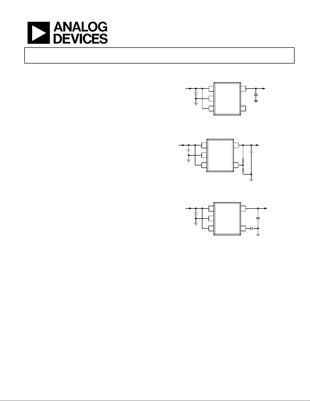
Figure 1. ADP1710 with Fixed Output Voltage, 3.3 V
= 5.5V
IN
1µF
Figure 2. ADP1710 with Adjustable Output Voltage, 0.8 V to 5.0 V
= 5V V
IN
1µF
Figure 3. ADP1711 with Fixed Output Voltage and Bypass Capacitor, 3.3 V
1
IN
2
GND
3
EN
NC = NO CONNECT
DP1710
ADJUSTABLE
1
IN
2
GND
3
EN
1
IN
2
GND
3
EN
ADP1710
OUT
OUT
ADJ
ADP1711
OUT
BYP
NC
V
5
4
= 3.3V
OUT
5
4
= 0.8V(1 + R1/R2)
OUT
1µF
R1
R2
= 3.3V
OUT
5
10nF
4
1µF
1µF
06310-001
06310-002
6310-003
GENERAL DESCRIPTION
The ADP1710/ADP1711 are low dropout linear regulators
that operate from 2.5 V to 5.5 V and provide up to 150 mA of
output current. Utilizing a novel scaling architecture, ground
current drawn is a very low 40 μA, when driving a 100 μA
load, making the ADP1710/ADP1711 ideal for batteryoperated portable equipment.
The ADP1710 and the ADP1711 are each available in sixteen
fixed output voltage options. The ADP1710 is also available in
an adjustable version, which allows output voltages that range
from 0.8 V to 5 V via an external divider. The ADP1711 allows
for a reference bypass capacitor to be connected, which reduces
output voltage noise and improves power supply rejection.
Rev. 0
Information furnished by Analog Devices is believed to be accurate and reliable. However, no
responsibility is assumed by Anal og Devices for its use, nor for any infringements of patents or ot her
rights of third parties that may result from its use. Specifications subject to change without notice. No
license is granted by implication or otherwise under any patent or patent rights of Analog Devices.
Trademarks and registered trademarks are the property of their respective owners.
The ADP1710/ADP1711 are optimized for stable operation with
small 1 μF ceramic output capacitors, allowing for good transient
performance while occupying minimal board space. An enable
pin controls the output voltage on both devices. There is also an
under-voltage lockout circuit on both devices, which disables the
regulator if IN drops below a minimum threshold.
An internal soft start gives a typical start-up time of 80 μs.
Short-circuit protection and thermal overload protection
circuits prevent damage to the devices in adverse conditions.
Both the ADP1710 and the ADP1711 are available in tiny
5lead TSOT packages, for the smallest footprint solution to all
your power needs.
One Technology Way, P.O. Box 9106, Norwood, MA 02062-9106, U.S.A.
Tel: 781.329.4700 www.analog.com
Fax: 781.461.3113 ©2006 Analog Devices, Inc. All rights reserved.

ADP1710/ADP1711
TABLE OF CONTENTS
Features .............................................................................................. 1
Applications....................................................................................... 1
Typical Applicat i o n C i rc uits ............................................................ 1
General Description......................................................................... 1
Revision History ............................................................................... 2
Specifications..................................................................................... 3
Absolute Maximum Ratings............................................................ 4
Thermal Resistance ...................................................................... 4
ESD Caution.................................................................................. 4
Pin Configurations and Function Descriptions ........................... 5
Typical Performance Characteristics ............................................. 6
Theory of Operation ........................................................................ 8
Adjustable Output Voltage (ADP1710 Adjustable) ................. 8
Bypass Capacitor (ADP1711)..................................................... 8
Enable Feature ...............................................................................8
Undervoltage L ockout (UVLO) ..................................................9
Application Information................................................................ 10
Capacitor Selection .................................................................... 10
Current Limit and Thermal Overload Protection ................. 10
Thermal Considerations............................................................ 11
Printed Circuit Board Layout Considerations ....................... 12
Outline Dimensions ....................................................................... 13
Ordering Guide .......................................................................... 14
REVISION HISTORY
10/06—Revision 0: Initial Version
Rev. 0 | Page 2 of 16

ADP1710/ADP1711
SPECIFICATIONS
VIN = (V
Table 1.
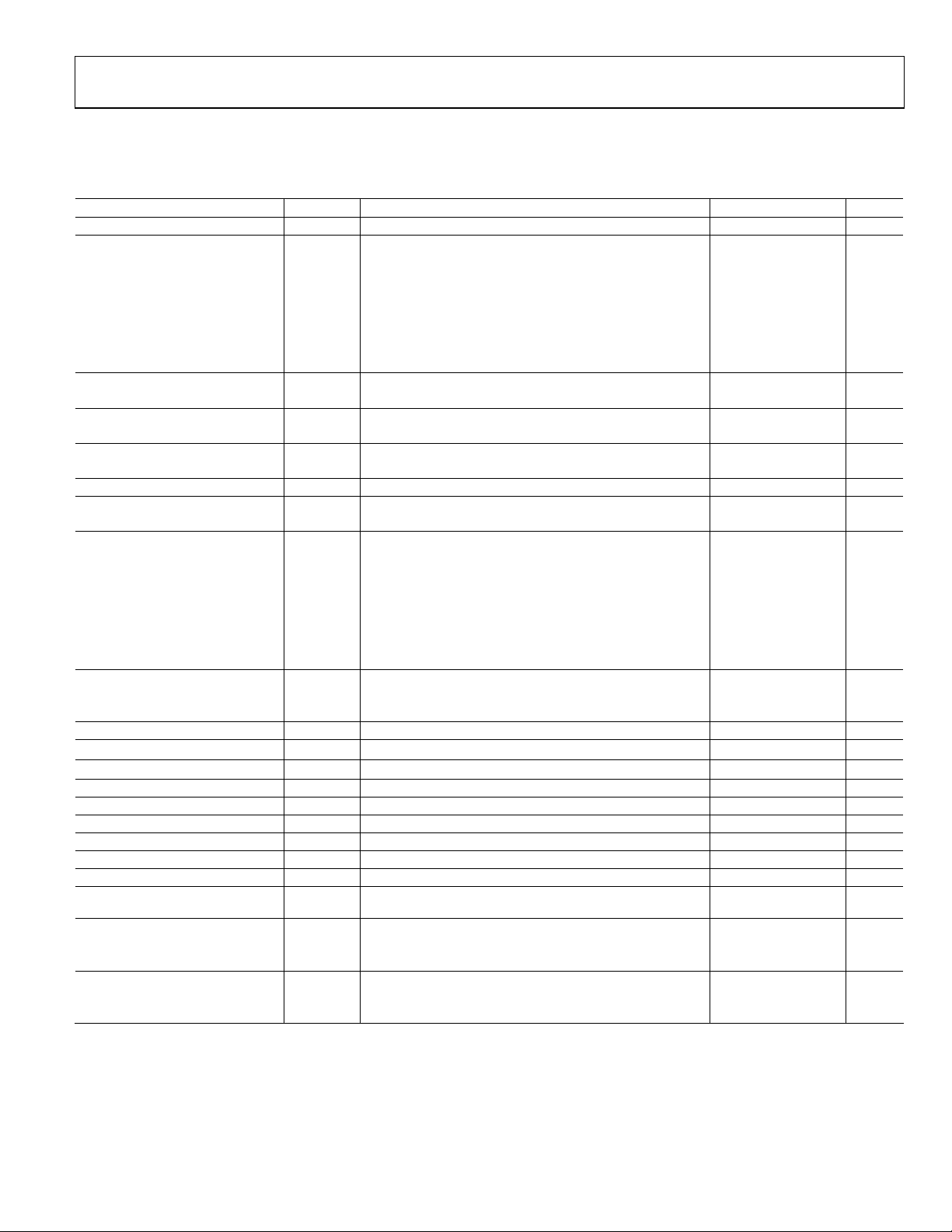
Parameter Symbol Conditions Min Typ Max Unit
INPUT VOLTAGE RANGE V
OPERATING SUPPLY CURRENT I
I
I
I
I
I
I
I
SHUTDOWN CURRENT I
EN = GND, TJ = –40°C to +125°C 1.0 μA
FIXED OUTPUT VOLTAGE ACCURACY V
(ADP1710 AND ADP1711) 100 μA < I
ADJUSTABLE OUTPUT VOLTAGE V
ACCURACY (ADP1710 ADJUSTABLE)1 100 μA < I
LINE REGULATION ∆V
LOAD REGULATION
I
DROPOUT VOLTAGE
I
I
I
I
I
I
I
START-UP TIME
ADP1710 80 μs
ADP1711 With 10 nF bypass capacitor 100 μs
CURRENT LIMIT THRESHOLD
THERMAL SHUTDOWN THRESHOLD TS
THERMAL SHUTDOWN HYSTERESIS TS
UVLO ACTIVE THRESHOLD UVLO
UVLO INACTIVE THRESHOLD UVLO
UVLO HYSTERESIS UVLO
EN INPUT LOGIC HIGH V
EN INPUT LOGIC LOW V
EN INPUT LEAKAGE CURRENT V
ADJ INPUT BIAS CURRENT
(ADP1710 ADJUSTABLE)
OUTPUT NOISE OUT
ADP1710 10 Hz to 100 kHz, V
ADP1711 10 Hz to 100 kHz, V
POWER SUPPLY REJECTION RATIO PSRR
ADP1710 1 kHz, V
ADP1711 1 kHz, V
1
Accuracy when OUT is connected directly to ADJ. When OUT voltage is set by external feedback resistors, absolute accuracy in adjust mode depends on the tolerances
of resistors used.
2
Based on an end-point calculation using 10 mA and 150 mA loads. See Figure 8 for typical load regulation performance for loads less than 10 mA.
3
Dropout voltage is defined as the input-to-output voltage differential when the input voltage is set to the nominal output voltage. This applies only for output
voltages above 2.5 V.
4
Start-up time is defined as the time between the rising edge of EN to OUT being at 90% of its nominal value.
5
Current limit threshold is defined as the current at which the output voltage drops to 90% of the specified typical value. For example, the current limit for a 1.0 V
output voltage is defined as the current that causes the output voltage to drop to 90% of 1.0 V, or 0.9 V.
+ 0.5 V) or 2.5 V (whichever is greater), I
OUT
IN
GND
GND-SD
OUT
OUT
/∆VINVIN = (V
2
3
4
5
OUT
∆V
OUT
V
DROPOUT
T
START-UP
I
LIMIT
SD
SD-HYS
IH
IL
I-LEAKAGE
ADJ
/∆I
OUTIOUT
ACTIVEVIN
INACTIVEVIN
HYS
I-BIAS
NOISE
= 1 mA, CIN = C
OUT
= 1 μF, TA = 25°C, unless otherwise noted.
OUT
TJ = –40°C to +125°C 2.5 5.5 V
I
= 0 μA 35 μA
OUT
= 0 μA, TJ = –40°C to +125°C 50 μA
OUT
= 100 μA 40 μA
OUT
= 100 μA, TJ = –40°C to +125°C 80 μA
OUT
= 100 mA 665 μA
OUT
= 100 mA, TJ = –40°C to +125°C 860 μA
OUT
= 150 mA 1 mA
OUT
= 150 mA, TJ = –40°C to +125°C 1.3 mA
OUT
EN = GND 0.1 μA
I
= 1 mA –1 +1 %
OUT
< 150 mA, TJ = –40°C to +125°C –2 +2 %
OUT
I
= 1 mA 0.792 0.8 0.808 V
OUT
< 150 mA, TJ = –40°C to +125°C 0.784 0.816 V
OUT
+ 0.5 V) to 5.5 V, TJ = –40°C to +125°C –0.1 +0.1 %/ V
OUT
= 10 mA to 150 mA 0.002 %/mA
= 10 mA to 150 mA, TJ = –40°C to +125°C 0.004 %/mA
OUT
I
= 100 mA, V
OUT
= 100 mA, V
OUT
= 150 mA, V
OUT
= 150 mA, V
OUT
= 100 mA, 2.5 V ≤ V
OUT
= 100 mA, 2.5 V ≤ V
OUT
= 150 mA, 2.5 V ≤ V
OUT
= 150 mA, 2.5 V ≤ V
OUT
≥ 3.0 V 100 mV
OUT
≥ 3.0 V, TJ = –40°C to +125°C 175 mV
OUT
≥ 3.0 V 150 mV
OUT
≥ 3.0 V, TJ = –40°C to +125°C 250 mV
OUT
< 3.0 V 120 mV
OUT
< 3.0 V, TJ = –40°C to +125°C 200 mV
OUT
< 3.0 V 180 mV
OUT
< 3.0 V, TJ = –40°C to +125°C 300 mV
OUT
180 270 360 mA
TJ rising 150
15
°C
°C
falling 1.95 V
rising 2.45 V
250 mV
2.5 V ≤ VIN ≤ 5.5 V 1.8 V
2.5 V ≤ VIN ≤ 5.5 V 0.4 V
EN = IN or GND 0.1 1 μA
30 100 nA
= 3.3 V 330 μVrms
OUT
= 0.75 V, with 10 nF bypass capacitor 40 μVrms
OUT
= 3.3 V 58 dB
OUT
= 0.75 V, with 10 nF bypass capacitor 69 dB
OUT
Rev. 0 | Page 3 of 16

ADP1710/ADP1711
ABSOLUTE MAXIMUM RATINGS
Table 2.
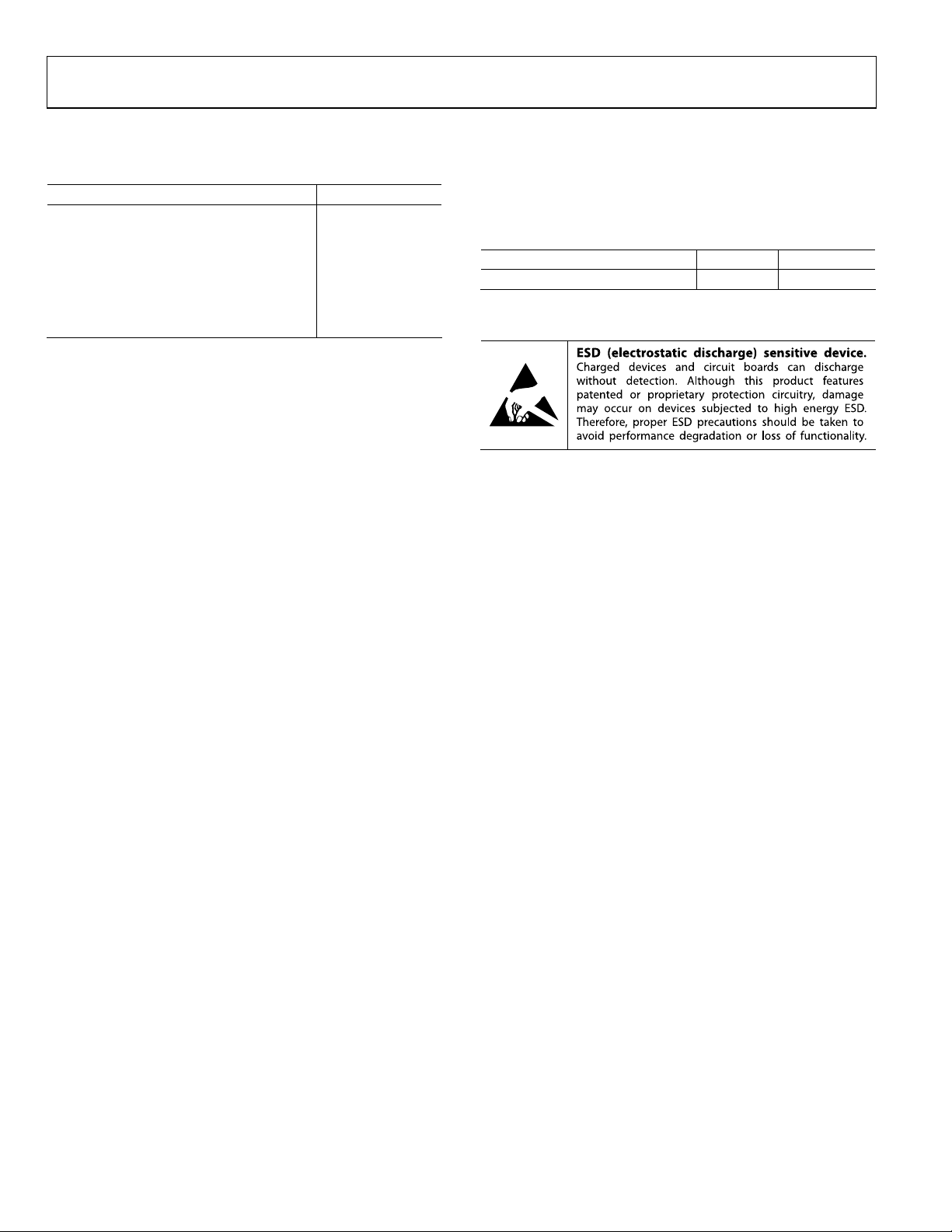
Parameter Rating
IN to GND –0.3 V to +6 V
OUT to GND –0.3 V to IN
EN to GND –0.3 V to +6 V
ADJ/BYP to GND –0.3 V to +6 V
Storage Temperature Range –65°C to +150°C
Operating Junction Temperature Range –40°C to +125°C
Soldering Conditions JEDEC J-STD-020
Stresses above those listed under Absolute Maximum Ratings
may cause permanent damage to the device. This is a stress
rating only; functional operation of the device at these or any
other conditions above those indicated in the operational
section of this specification is not implied. Exposure to absolute
maximum rating conditions for extended periods may affect
device reliability.
THERMAL RESISTANCE
θJA is specified for the worst-case conditions, that is, a device
soldered in a circuit board for surface-mount packages.
Table 3. Thermal Resistance
Package Type θ
5-Lead TSOT 170 °C/W
JA
Unit
ESD CAUTION
Rev. 0 | Page 4 of 16

ADP1710/ADP1711
G
G
PIN CONFIGURATIONS AND FUNCTION DESCRIPTIONS
1
IN
ADP1710
FIXED
2
ND
TOP VIEW
(Not to Scale)
3
EN
NC = NO CONNECT
5
OUT
4
NC
06310-004
IN
ND
EN
1
ADP1710
ADJUSTABLE
2
TOP VIEW
(Not to S cale)
3
5
OUT
4
ADJ
06310-005
GND
EN
1
IN
2
3
ADP1711
TOP VIEW
(Not to S cal e)
5
OUT
4
BYP
06310-006
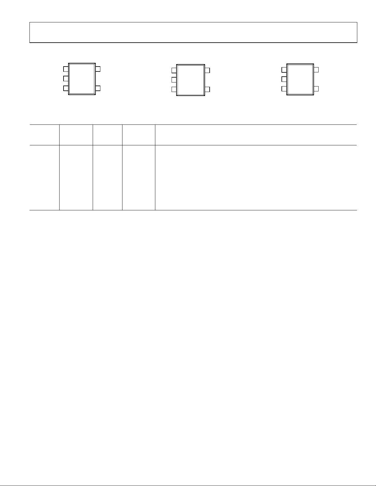
Figure 4. 5-Lead TSOT (UJ-Suffix) Figure 5. 5-Lead TSOT (UJ-Suffix) Figure 6. 5-Lead TSOT (UJ-Suffix)
Table 4. Pin Function Descriptions
ADP1710
Fixed
Pin No.
ADP1710
Adjustable
Pin No.
ADP1711
Pin No.
Mnemonic Description
1 1 1 IN Regulator Input Supply. Bypass IN to GND with a 1 μF or greater capacitor.
2 2 2 GND Ground.
3 3 3 EN
Enable Input. Drive EN high to turn on the regulator; drive it low to turn off the
regulator. For automatic startup, connect EN to IN.
4 NC No Connect.
4 ADJ Adjust. A resistor divider from OUT to ADJ sets the output voltage.
4 BYP
Connect a 1 nF or greater capacitor (10 nF is recommended) between BYP and GND
to reduce the internal reference noise for low noise applications.
5 5 5 OUT Regulated Output Voltage. Bypass OUT to GND with a 1 μF or greater capacitor.
Rev. 0 | Page 5 of 16
 Loading...