Dual LED Flash Driver with
http://www.BDTIC.com/ADI
FEATURES
Ultracompact solution
Small 2 mm × 1.5 mm 12-ball WLCSP package
Tiny, low profile 2.2 H power inductor
LED current source for local LED grounding and low EMI
Synchronous 2 MHz PWM boost convertor, no external diode
High efficiency: 88% peak
Reduces high levels of input battery current during flash
Limits battery current drain in torch mode
2
I
C programmable
Currents up to 400 mA in flash mode for two LEDs
Currents up to 500 mA in flash mode for one LED with
5% accuracy
Currents up to 160 mA in torch mode with 10% accuracy
Peak inductor current limit
Flash timer
Control
2
I
C-compatible control registers
External STROBE pin
External direct TORCH pin
TX_MASK input to prevent high input battery current levels
Safety
Thermal overload protection
Flash timeout
Inductor fault detection
Output overvoltage
Short circuit protection
Soft start reduces inrush input current
I2C-Compatible Interface
ADP1655
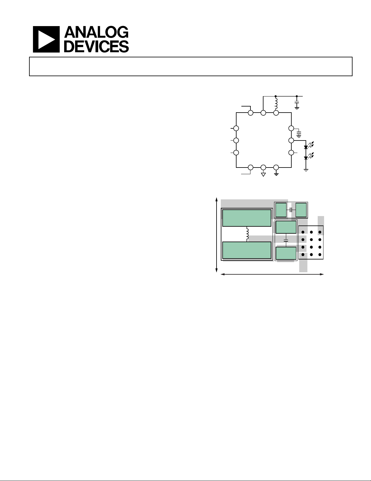
FUNCTIONAL BLOCK DIAGRAM
INPUT VOLTAGE = 2.5V TO 5.5V
2.2µH
STROBE VIN SW
TORCH
ADP1655
SCL/EN1
SDA/EN2
I2C/EN SGND PGND
VOUT
LED_OUT
TX_MASK
Figure 1.
Li-ION +
C1
L1
3mm
INDUCTOR
6.5mm
Figure 2. PCB Layout
10µF
10µF
8028-001
PGND
C2
LED
ANODE
Li-ION +
DIGITAL
INPUT/
OUTPUT
08028-002
APPLICATIONS
Camera-enabled cellular phones and smart phones
Digital still cameras, camcorders, and PDAs
GENERAL DESCRIPTION
The ADP1655 is a very compact, highly efficient, dual white
LED flash driver for high resolution camera phones, which
improves picture and video quality in low light environments.
The device integrates a 2 MHz synchronous inductive boost
convertor, an I
source. The high switching frequency enables the use of a tiny,
low profile 2.2 µH power inductor, and the current source
permits LED cathode grounding for thermally enhanced,
low EMI and compact layouts.
The efficiency is high over the entire battery voltage range to
maximize the input power to LED power conversion and
Rev. 0
Information furnished by Analog Devices is believed to be accurate and reliable. However, no
responsibility is assumed by Analog Devices for its use, nor for any infringements of patents or other
rights of third parties that may result from its use. Specifications subject to change without notice. No
license is granted by implication or otherwise under any patent or patent rights of Analog Devices.
Trademarks and registered trademarks are the property of their respective owners.
2
C-compatible interface and a 500 mA current
minimize battery current draw during flash events. In addition,
a Tx-mask input permits the flash LED current to reduce quickly
and, therefore, the battery current reduces quickly, during a
GSM power amplifier current burst.
2
The I
C-compatible interface enables the programmability
of timers, currents, and status bit readback for operation
monitoring and safety control.
The ADP1655 comes in a compact 12-ball 0.5 mm pitch
WLCSP package and is specified over the full −40°C to
+125°C junction temperature range.
One Technology Way, P.O. Box 9106, Norwood, MA 02062-9106, U.S.A.
Tel: 781.329.4700 www.analog.com
Fax: 781.461.3113 ©2009 Analog Devices, Inc. All rights reserved.

ADP1655
http://www.BDTIC.com/ADI
TABLE OF CONTENTS
Features .............................................................................................. 1
Applications ....................................................................................... 1
Functional Block Diagram .............................................................. 1
General Description ......................................................................... 1
Revision History ............................................................................... 2
Specifications ..................................................................................... 3
Recommended Specifications: Input and Output Capacitance
and Inductance ............................................................................. 4
I2C-Compatible Interface Timing Specifications ..................... 5
Absolute Maximum Ratings ............................................................ 6
Thermal Data ................................................................................ 6
Thermal Resistance ...................................................................... 6
ESD Caution .................................................................................. 6
Pin Configuration and Function Descriptions ............................. 7
Typical Performance Characteristics ............................................. 8
Theory of Operation ...................................................................... 12
White LED Driver ...................................................................... 12
Assist Light and Torch Modes .................................................. 12
2-Bit Logic Interface Mode (I2C/EN = 0) ............................... 13
I2C Interface Mode (I2C/EN = 1) ............................................. 13
State Transitions ......................................................................... 15
I2C Register Map ............................................................................. 16
Safety Features ................................................................................. 19
Overvoltage Fault ....................................................................... 19
Output Capacitor Fault .............................................................. 19
Timeout Fault .............................................................................. 19
Overtemperature Fault .............................................................. 19
Short-Circuit Fault ..................................................................... 19
Current Limit .............................................................................. 19
Amount of LED Detection ........................................................ 19
Input Undervoltage .................................................................... 19
Applications Information .............................................................. 20
External Component Selection ................................................ 20
PCB Layout ...................................................................................... 22
Outline Dimensions ....................................................................... 23
Ordering Guide .......................................................................... 23
REVISION HISTORY
5/09—Revison 0: Initial Version
Rev. 0 | Page 2 of 24

ADP1655
http://www.BDTIC.com/ADI
SPECIFICATIONS
VIN = 3.6 V, TJ = −40°C to +125°C for minimum/maximum specifications and TA = 25°C for typical specifications, unless
otherwise noted.
Table 1.
Parameter1 Conditions Min Typ Max Unit
SUPPLY
Input Voltage Range 2.7 5.5 V
Undervoltage Lockout Threshold VIN falling 2.3 2.4 2.5 V
Hysteresis 50 100 150 mV
Shutdown Current TJ = −40°C to +85°C, current into VIN pin, VIN = 2.7 V to 4.5 V 0.3 1 μA
Standby Current TJ = −40°C to +85°C, current into VIN pin, VIN = 2.7 V to 4.5 V 3 10 μA
I2C/EN = SCL/EN1 = SDA/EN2 = 1.8 V
Operating Quiescent Current Torch mode, two LEDs, LED current = 40 mA 5.3 mA
SW Switch Leakage TJ = −40°C to +85°C 1 μA
INPUTS
Input Logic Low Voltage 0.54 V
Input Logic High Voltage 1.26 V
TORCH, STROBE, TX_MASK Pull-Down 350 kΩ
SCL/EN1, SDA/EN2 Pull-Down I2C/EN = 0 V 350 kΩ
TORCH Glitch Filtering Delay From TORCH rising edge to device start 6.3 9 11.7 ms
LED DRIVER
LED Current
Assist Light, Torch I2C/EN = 0, one LED 80 mA
I2C/EN = 0, two LEDs 40 mA
I2C/EN = 1, assist light value setting = 0 (000 binary) 20 mA
I2C/EN = 1, assist light value setting = 7 (111 binary) 160 mA
Flash I2C/EN = 0, one LED 500 mA
I2C/EN = 0, two LEDs 320 mA
I2C/EN = 1, flash value setting = 0 (0000 binary) 200 mA
I2C/EN = 1, one LED, flash value setting = 15 (1111 binary) 500 mA
LED Current Accuracy I
I
I
LED Current Source Headroom2 Flash typical, 400 mA LED current 290 mV
Torch 160 mA 190
LED_OUT Ramp-Up Time 1 ms
LED_OUT Ramp-Down Time 0.5 ms
Maximum Timeout For Flash 850 ms
Timer Accuracy −7.5 +7.5 %
SWITCHING REGULATOR
Switching Frequency 1.85 2 2.15 MHz
Minimum Duty Cycle 9.0 %
N-FET Resistance 135 mΩ
P-FET Resistance 290 mΩ
I2C/EN = 1, two LEDs, flash value setting = 10 to 15 (1010 to
1111 binary)
= 320 mA to 500 mA −5 +5 %
LED
= 60 mA to 320 mA −5 +10 %
LED
= 20 mA to 60 mA −5 +20 %
LED
400 mA
Rev. 0 | Page 3 of 24

ADP1655
http://www.BDTIC.com/ADI
Parameter1 Conditions Min Typ Max Unit
SAFETY FEATURES
Thermal Shutdown Threshold
TJ Rising 150 °C
TJ Falling 140 °C
Overvoltage Threshold 9.0 9.5 10.1 V
Coil Peak Current Limit Peak current value setting = 0 (00 binary) 1.13 1.25 1.38 A
Peak current value setting = 1 (01 binary) 1.35 1.5 1.65 A
Peak current value setting = 2 (10 binary) 1.58 1.75 1.93 A
Peak current value setting = 3 (11 binary) 1.8 2.0 2.2 A
LED_OUT Short-Circuit Detection
Comparator Reference Voltage
LED Counting Comparator
Threshold Voltage
LED value setting = 0 (00 binary) 4.3 V
LED value setting = 1 (01 binary) 4.6 V
LED value setting = 2 (10 binary) 4.0 V
LED value setting = 3 (11 binary) 4.9 V
1
All limits at temperature extremes are guaranteed via correlation using standard statistical quality control (SQC).
2
Two LEDs are used for this parameter.
RECOMMENDED SPECIFICATIONS: INPUT AND OUTPUT CAPACITANCE AND INDUCTANCE
1.2 1.3 V
Table 2.
Parameter Symbol Conditions Min Typ Max Unit
CAPACITANCE C
Input TA = −40°C to +125°C 4.0 μF
Output TA = −40°C to +125°C 4.0 20 μF
MINIMUM AND MAXIMUM INDUCTANCE L TA = −40°C to +125°C 1.5 2.8 μH
MIN
Rev. 0 | Page 4 of 24

ADP1655
A
http://www.BDTIC.com/ADI
I2C-COMPATIBLE INTERFACE TIMING SPECIFICATIONS
Table 3.
Parameter1 Min Max Unit Description
f
SCL
t
HIGH
t
LOW
t
SU, DAT
t
0 0.9 μs Data hold time
HD, DAT
t
SU, STA
t
HD, STA
t
BUF
t
SU, STO
tR 20 + 0.1 C
tF 20 + 0.1 C
t
SP
CB 400 pF Capacitive load for each bus line
1
Guaranteed by design.
2
CB is the total capacitance of one bus line in picofarads.
400 kHz SCL clock frequency
0.6 μs SCL high time
1.3 μs SCL low time
100 ns Data setup time
0.6 μs Setup time for repeated start
0.6 μs Hold time for start/repeated start
1.3 μs Bus free time between a stop and a start condition
0.6 μs Setup time for stop condition
2
300 ns Rise time of SCL and SDA
B
B
300 ns Fall time of SCL and SDA
0 50 ns Pulse width of suppressed spike
SD
t
LOW
SCL
S
S = START CONDITION
Sr = REPEATED ST ART CONDITI ON
P = STOP CO NDITION
t
R
t
HD, DAT
t
SU, DAT
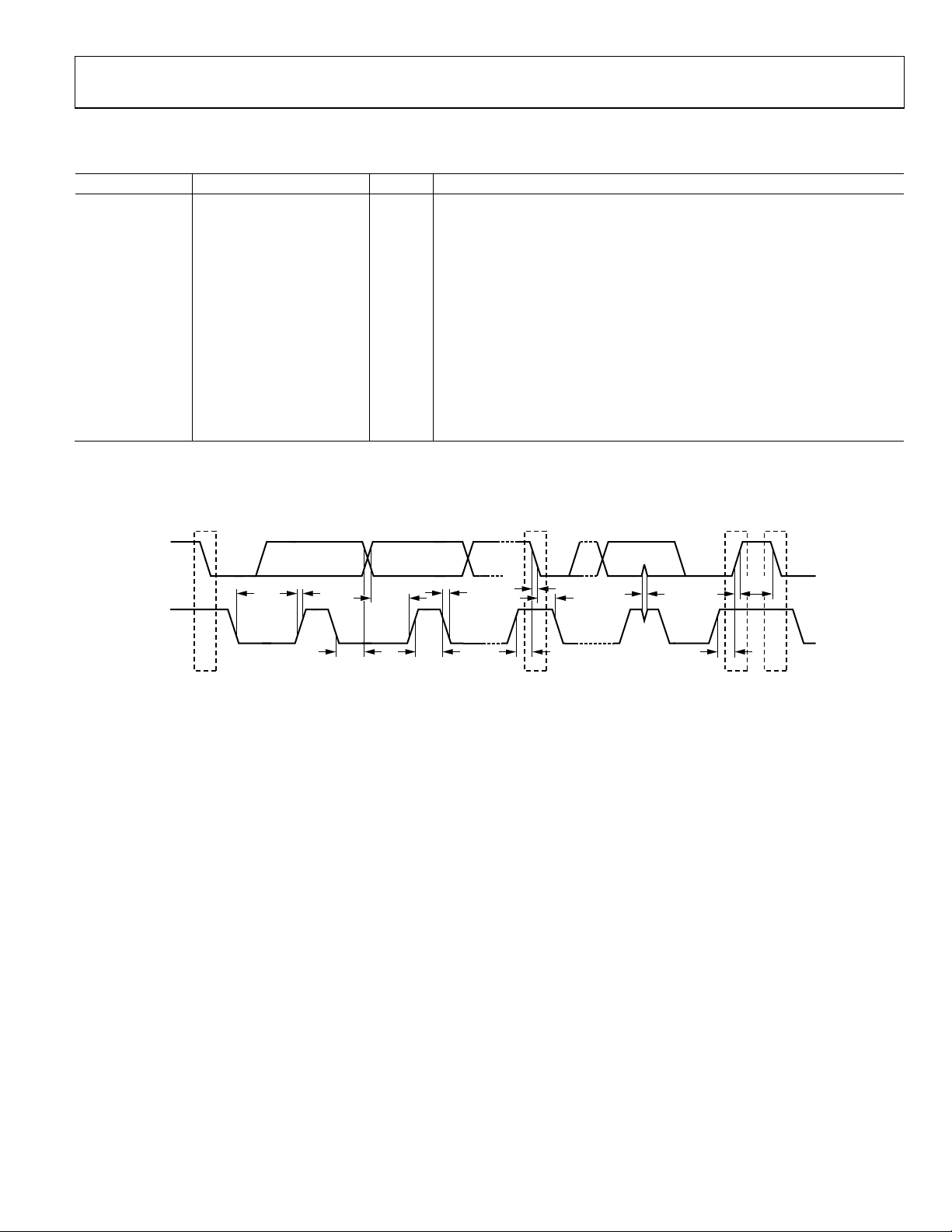
Figure 3. I
t
F
t
F
t
HIGH
2
C-Compatible Interface Timing Diagram
t
SU, STA
t
HD, STA
Sr P S
t
SP
t
SU, STO
t
BUF
t
R
08028-003
Rev. 0 | Page 5 of 24

ADP1655
http://www.BDTIC.com/ADI
ABSOLUTE MAXIMUM RATINGS
Table 4.
Parameter Rating
VIN, SDA/EN2, SCL/EN1, I2C/EN,
STROBE, TORCH, TX_MASK to SGND
LED_OUT, SW, VOUT to SGND −0.3 V to +12 V
PGND to SGND −0.3 V to +0.3 V
VOUT to LED_OUT −0.3 V to +6 V
Ambient Temperature Range (TA) −40°C to +85°C
Junction Temperature Range (TJ) −40°C to +125°C
Storage Temperature JEDEC J-STD-020
ESD Human Body Model ±2000 V
ESD Charged Device Model ±1000 V
ESD Machine Model ±200 V
−0.3 V to +6 V
Stresses above those listed under Absolute Maximum Ratings
may cause permanent damage to the device. This is a stress
rating only; functional operation of the device at these or any
other conditions above those indicated in the operational
section of this specification is not implied. Exposure to absolute
maximum rating conditions for extended periods may affect
device reliability.
THERMAL DATA
The ADP1655 may be damaged if the junction temperature
limits are exceeded. Monitoring T
is within the specified temperature limits. In applications with
high power dissipation and poor thermal resistance, the maximum
T
may have to be derated. In applications with moderate power
A
dissipation and low PCB thermal resistance, the maximum T
can exceed the maximum limit as long as the T
fication limits. T
of the device is dependent on the TA, the power
J
dissipation (PD) of the device, and the junction-to-ambient
thermal resistance (θ
calculated from the T
= TA + (PD × θJA)
T
J
) of the package. Maximum TJ is
JA
and PD using the following formula:
A
does not guarantee that TJ
A
is within speci-
J
A
THERMAL RESISTANCE
θJA of the package is based on modeling and calculation using
a 4-layer board. θ
is highly dependent on the application and
JA
board layout. In applications where high maximum power dissipation exists, attention to thermal board design is required. The
value of θ
environmental conditions. The specified value of θ
may vary, depending on PCB material, layout, and
JA
is based
JA
on a 4-layer, 4 in × 3 in, 2 1/2 oz copper board, per JEDEC
standards. For more information, see the AN-617 Application
Note, MicroCSP
θ
is specified for a device mounted on a JEDEC 2S2P PCB.
JA
TM
Wafer Level Chip Scale Package.
Table 3. Thermal Resistance
Package Type θJA Unit
12-Ball WLCSP 75 °C/W
ESD CAUTION
Rev. 0 | Page 6 of 24

ADP1655
http://www.BDTIC.com/ADI
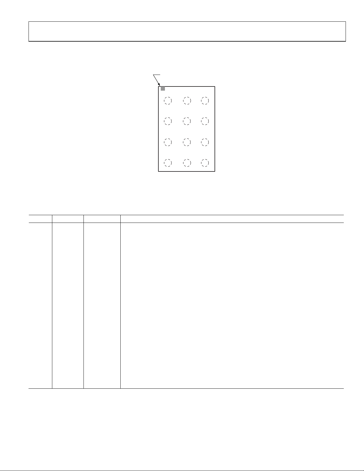
PIN CONFIGURATION AND FUNCTION DESCRIPTIONS
BALLA1
INDICATOR
1
PGND SGND VIN
A
23
SW
B
VOUT STROBE I2C/EN
C
LED_OUT SDA/EN2 SCL/EN1
D
(BALL SIDE DO WN)
Not to Scale
Figure 4. Pin Configuration
TORCH
TOP VIEW
TX_MASK
08028-004
Table 5. Pin Function Descriptions
Pin No. Mnemonic Type Description
A1 PGND Ground Ground for Internal Switching FET.
A2 SGND Ground Connect this pin at a single point to the power ground.
A3 VIN Supply
Connect the battery between VIN and PGND. Bypass VIN with a 10 μF, 6.3 V or greater X5R/X7R
capacitor.
B1 SW Output Connect a 2.2 μH inductor between SW and the battery.
B2 TORCH Digital Input This pin enables the torch, provided that the device is not in flash or assist light mode.
B3 TX_MASK Digital Input
Connect a digital signal to the TX_MASK pin. When the logic level is driven high during a flash
event the current is reduced to the torch level.
C1 VOUT Output
VOUT senses the output voltage of the boost converter and provides the input voltage to the LED
current source. The VOUT pin features a comparator to detect an overvoltage condition if the LED
string is open circuited. Connect a 10.0 μF capacitor between VOUT and PGND.
C2 STROBE
Digital Input/
Output
The STROBE input is used to synchronize the timing of the camera module to the LED driver in
2
I
C-compatible interface mode. In 2-bit logic interface mode, this acts as an output, indicating the
number of LEDs attached. STROBE = high indicates two LEDs, whereas STROBE = low indicates
one LED.
C3 I2C/EN Digital Input
A logic low selects the 2-bit logic interface, whereas logic high selects I
2
C-compatible interface. If
I2C/EN is low and SDA/EN2 and SCL/EN1 are low, the driver enters shutdown mode with
consumption < 1 μA.
D1 LED_OUT Output
White LED Anode Connection. Connect LED_OUT to the anode of the white LED. LED_OUT is
internally connected to a programmable PMOS current source, which regulates the LED current.
D2 SDA/EN2
D3 SCL/EN1 Digital Input
Digital Input/
Output
Data Input/Output (SDA). In 2-bit logic interface mode, SDA/EN2 is the second input bit of the
digital interface.
Second Input Bit (EN2). In I
Clock Input (SCL). In 2-bit logic interface mode, SCL/EN1 is the first input bit of the digital interface.
First Input Bit (EN1). In I
2
C mode, SDA is the data input/output of the I2C-compatible interface.
2
C mode, SCL is the clock input of the I2C-compatible interface.
Rev. 0 | Page 7 of 24
 Loading...