Compact, High Efficiency, High Power,
www.BDTIC.com/ADI
Flash/Torch LED Driver with Dual Interface
FEATURES
Small 6.4 mm × 7.2 mm solution
2.2 H power inductor
92% peak efficiency
Tx masking within 50 s
2.1 A, 12 V power switch
Pin-selectable interface: 2-bit logic or I
Programmable flash and torch current
Up to 200 mA in torch mode
Up to 500 mA in flash mode
Programmable indicator LED current up to 20 mA
Programmable timer register: up to 820 ms flash timeout
2.75 V to 5.5 V input voltage range
Low noise, 1.2 MHz PWM operation
Safety features
Interrupt output pin
Fault condition register
S
hort-circuit protection
Output overvoltage protection
Thermal overload protection
Integrated current limit and soft start
Small 3 mm × 3 mm, 16-lead LFCSP footprint
APPLICATIONS
Camera-enabled cellular phones, smart phones
Digital still cameras, camcorders, PDAs
2
C
ADP1653
GENERAL DESCRIPTION
The ADP1653 is a very compact, high efficiency, high power,
camera flash LED driver optimized for cellular phones. The
high efficiency and dynamic LED current control of the device
improve flash brightness and picture quality in dimly lit
environments. Efficiency peaks at 92% and is higher than
charge pump solutions over the Li-Ion battery range.
The device has a dual-mode interface that is configurable to 2-bit
log
ic or an I
currents are programmable with external resistors or through the
2
I
C interface. To maximize overall flash brightness, the ADP1653
offers an input to reduce flash LED current in less than 50 µs,
referred to as the Tx mask. Tx masking reduces battery stress by
scaling back flash LED current during an RF transmission.
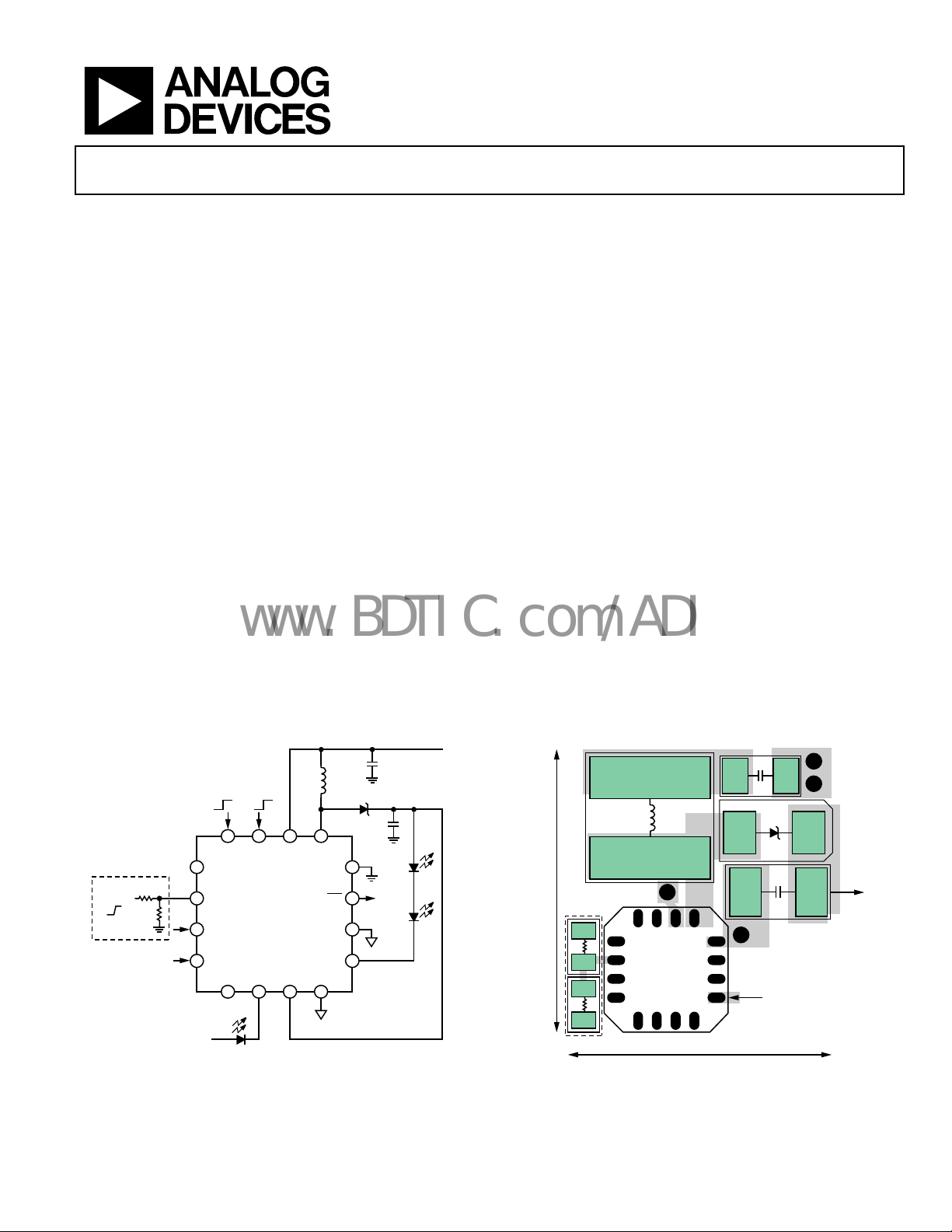
The ADP1653 solution requires only four external components
2
in I
grates multiple safety features such as soft start, flash timeout,
output current limit, thermal protection, and overvoltage
protection.
The ADP1653 operates over the −40°C to +125°C junction
t
emperature range.
2
C® interface. The indicator and high power LED
C mode and fits in a 6.4 mm × 7.2 mm space. The part inte-
TYPICAL OPERATING CIRCUIT
INPUT VOLTAGE = 2.75V TO 5.5V
4.7µF
ON
16 15 14 13
STR
EN
V
ADP1653
OUT
ILED
SETI
5 6 7 8
OPTIONAL
TxMASK
OFFONOFF
1
SETT
2
SETF
3
CTRL1/SCL
4
CTRL0/SDA
V
DD
Figure 1.
Rev. B
Information furnished by Analog Devices is believed to be accurate and reliable. However, no
responsibility is assumed by Anal og Devices for its use, nor for any infringements of patents or ot her
rights of third parties that may result from its use. Specifications subject to change without notice. No
license is granted by implication or otherwise under any patent or patent rights of Analog Devices.
Trademarks and registered trademarks are the property of their respective owners.
2.2µH
UP TO 10.2V
4.7µF
LX
DD
PGND
INT
INTF
HPLED
GND
12
ONE
OR
TWO
11
LEDs
10
9
06180-001
PCB LAYOUT
LI-ION +
INDUCTOR
L1
7.2mm
R5
INPUT CAPACIT OR
C1
SCHOTTKY DI ODE
PGND
ADP1653
R4
OPTIO NAL (Tx MAS K ONLY)
6.4mm
FROM WHITE
LEDs
Figure 2.
One Technology Way, P.O. Box 9106, Norwood, MA 02062-9106, U.S.A.
Tel: 781.329.4700 www.analog.com
Fax: 781.461.3113 ©2007 Analog Devices, Inc. All rights reserved.
GND
D1
C2
OUTPUT CAPACI TOR
L = FDSE0312- 2R2
CIN = GRM219R61A475K
D1 = BAT20J
COUT = GRM21BR61C475K
TO WHITE
LEDs
6180-036

ADP1653
www.BDTIC.com/ADI
TABLE OF CONTENTS
Features .............................................................................................. 1
Applications....................................................................................... 1
General Description......................................................................... 1
Typical O p erating Ci rc u it ................................................................ 1
PCB Layout........................................................................................ 1
Revision History ............................................................................... 2
Specifications..................................................................................... 3
2
I
C Timing Specifications............................................................ 5
Absolute Maximum Ratings............................................................ 6
Thermal Resistance ...................................................................... 6
Boundary Condition .................................................................... 6
ESD Caution.................................................................................. 6
Pin Configuration and Function Descriptions............................. 7
REVISION HISTORY
9/07—Rev. A to Rev. B
Changes to Table 1............................................................................ 3
Changes to Table 5............................................................................ 7
Changes to I
Changes to Safety Features Section .............................................. 16
Inserted Table 9 and Table 10........................................................ 18
Inserted Table 11 and Table 12...................................................... 19
1/07—Revision A: Initial Version
2
C Interface Mode (INTF = 0) Section .................. 14
Typical Perfor m an c e Charac t e r istics ..............................................9
Theory of Operation ...................................................................... 13
White LED Driver...................................................................... 13
2-Bit Logic Interface Mode (INTF = 1)................................... 14
2
I
C Interface Mode (INTF = 0)................................................. 14
Turning on the Flash and Watchdog Timer ........................... 15
Safety Features ............................................................................ 16
Applications Information.............................................................. 17
Flash Current Foldback During Transmit Pulse.................... 17
External Component Selection ................................................ 18
PCB Layout ................................................................................. 20
Outline Dimensions ....................................................................... 22
Ordering Guide .......................................................................... 22
Rev. B | Page 2 of 24
ADP1653
www.BDTIC.com/ADI
SPECIFICATIONS
VDD = 3.0 V to 5.5 V, TJ = −40°C to +125°C, unless otherwise noted.
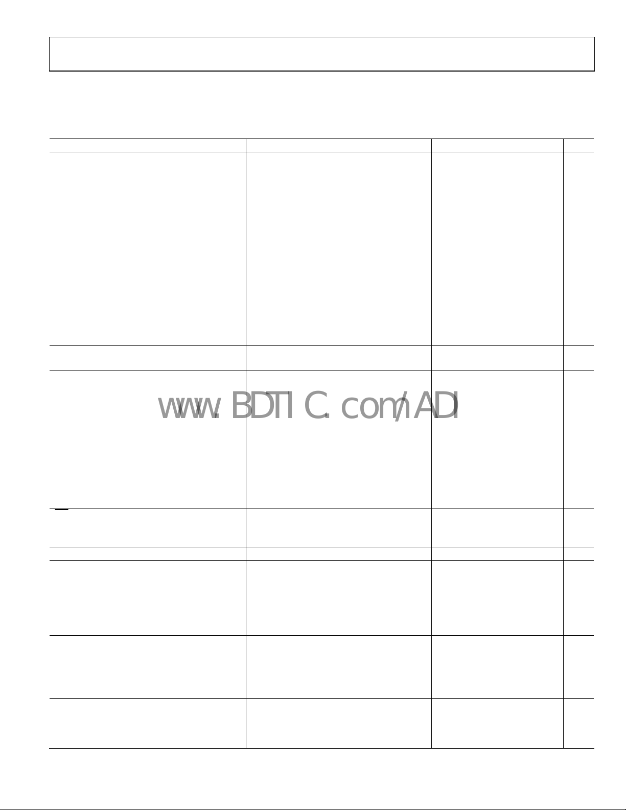
Table 1.
Parameter Conditions Min Typ Max Unit
SUPPLY
Input Voltage Range
2
3.0 5.5 V
Undervoltage Lockout Threshold VDD rising 2.80 2.9 2.95 V
V
falling 2.58 2.7 2.75 V
DD
Shutdown Current EN = GND, TJ = −40°C to +85°C 0.1 1 μA
Soft Power-Down Current
INTF = 0, EN = VDD, ILED register = 0,
HPLED register = 0, T
INTF = 1, EN = V
= −40°C to +85°C
T
J
INTF = 0, EN = VDD, ILED register = 001,
Operating Current
3
HPLED register = 0
INTF = 1, (CTRL1, CTRL0) = (0, 1), R
INTF = 0, EN = VDD, HPLED register = 00001 1.6 3 mA
INTF = 1, (CTRL1, CTRL0) = (1, x) 1.6 3 mA
LX Leakage TJ = −40°C to +85°C 0.05 0.5 μA
HPLED Leakage TJ = −40°C to +85°C 0.03 0.5 μA
THERMAL SHUTDOWN
Thermal Shutdown Threshold TJ rising 155 °C
INPUTS
EN, STR, CTRL1/SCL, CTRL0/SDA
Input Logic Low Voltage TJ = −40°C to +85°C 0.54 V
T
= −40°C to +125°C 0.48 V
J
Input Logic High Voltage TJ = −40°C to +85°C 1.26 V
T
= −40°C to +125°C 1.27 V
J
SETI, SETT, SETF
Input Logic High Voltage 1.4 V
INTF
Input Logic Low Voltage
Input Logic High Voltage
INT OUTPUT
Logic Low Output Voltage I
4
4
V
V
= −3 mA 0.4 V
SINK
Logic High Leakage Current 0.05 0.5 μA
SETI, SETT, SETF REFERENCE VOLTAGE 1.19 1.22 1.24 V
INDICATOR LED
Current Sink Headroom V
R
R
= VDD − VF (ILED) 1 V
HEADROOM
= 25 kΩ 14.5 17.5 21.5 mA INTF = 1, SETI Current Source
SETI
= 200 kΩ 2.0 2.5 3.0 mA
SETI
ILED register = 1 (001 binary), SETI = V
ILED register = 7 (111 binary), SETI = V
WHITE LED DRIVER
LX
Switching Frequency 1.1 1.2 1.3 MHz
Current Limit 1.8 2.1 2.45 A
On Resistance 250 420 mΩ
OUT
Soft Start Ramp 18 V/ms
Overvoltage Threshold VDD rising 9.8 10.15 10.5 V
Bias Current
5
V
= 10 V 12 μA
OUT
1
= −40°C to +85°C
J
, (CTRL1, CTRL0) = (0, 0),
DD
= 200 kΩ 500 700 μA
SETI
19 45 μA
19 45 μA
500 700 μA
/2 − 0.6 V
DD
/2 + 0.6 V
DD
DD
DD
2.0 2.5 3.0 mA INTF = 0
14.5 17.5 21.5 mA
Rev. B | Page 3 of 24
ADP1653
www.BDTIC.com/ADI
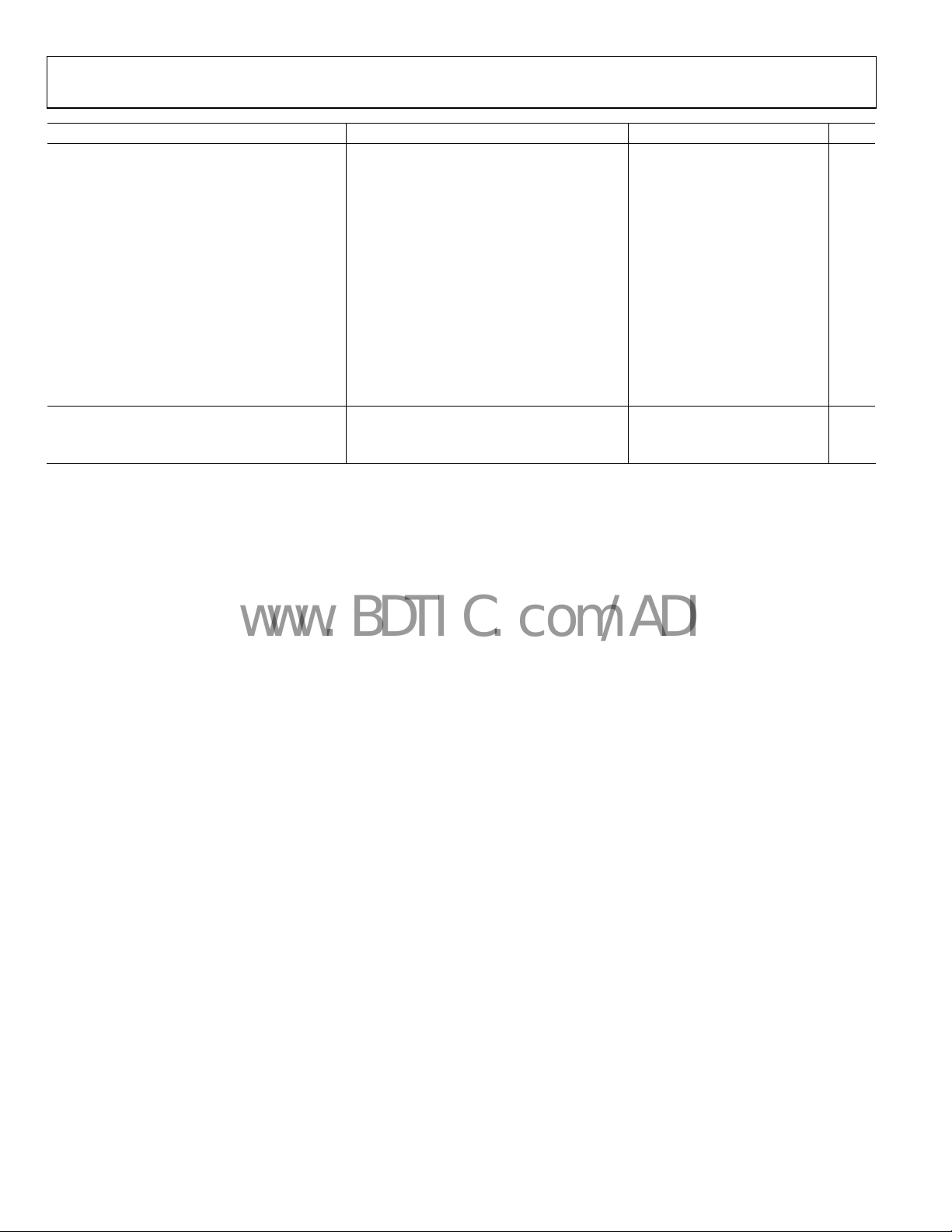
Conditions Min Typ Max Unit Parameter
HPLED
Regulation Voltage
Regulation Current
INTF = 1, Torch Mode RSETT = 50 kΩ or SETT = V
RSETT = 125 kΩ 35 50 60 mA
Flash Mode RSETF = 50 kΩ 460 500 550 mA
RSETF = 500 kΩ 35 50 60 mA
INTF = 0, Flash Mode HPLED register = 11111 (binary), SETF = V
HPLED register = 11000 (binary), SETF = V
Torch Mode HPLED register = 00110 (binary), SETF = V
HPLED register = 00001 (binary), SETF = V
Step Size for HPLED LSB Change SETF = V
Maximum Flash Timeout INTF = 0 or 1, 983,040 × oscillator cycles 820 ms
SETF RESPONSE (TRANSMIT MASKING FUNCTION)7
HPLED current = 335 mA to 140 mA 22 μs
HPLED current = 140 mA to 335 mA 24 μs
1
All limits at temperature extremes are guaranteed via correlation using standard statistical quality control (SQC). Typical values are at TA = 25°C, VDD = 3.6 V.
2
This is the VDD input voltage range over which the rest of the specifications are valid. The part operates as expected until VDD goes below the UVLO threshold.
3
This is the current into the VDD pin. Additional current can flow into the indicator LED or HPLED, depending on the mode selected.
4
INTF should be tied to GND (INTF = 0) for I2C interface or to VDD (INTF = 1) for hardwire interface. All other digital inputs are 1.8 V compatible.
5
This bias current is active only when the high power LED and/or indicator LED functions are enabled.
6
This specification is not valid during minimum on-time operation of the boost converter (one LED case) when excess voltage is dropped across the HPLED pin.
7
This specification is not production tested but is based on bench evaluation. It is based on the typical two-LED application circuit using a 100 kΩ resistor from SETF to GND,
and a 160 kΩ resistor to a 1.8 V Tx mask logic signal with <1 μs rise/fall time. HPLED register = 11001 (binary). The inductor current has settled to within ±5% of final value.
6
Boost active, two high power LEDs (HPLEDs)
0.23 0.32 0.42 V
in series
DD
DD
110 125 145 mA
460 500 550 mA
DD
365 395 435 mA
DD
110 125 145 mA
DD
38 50 60 mA
DD
15 mA
Rev. B | Page 4 of 24
ADP1653
www.BDTIC.com/ADI
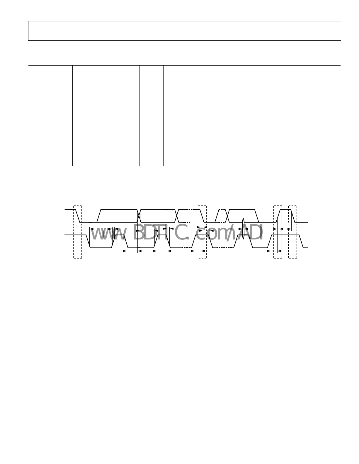
I2C TIMING SPECIFICATIONS
Table 2.
Parameter Min Max Unit Description
f
SCL
t
HIGH
t
LOW
t
SU, DAT
1
t
HD, DAT
t
SU, STA
t
HD, STA
t
BUF
t
SU, STO
t
R
t
F
t
SP
2
C
B
1
A master device must provide a hold time of at least 300 ns for the SDA signal (referred to the VIH minimum of the SCL signal) to bridge the undefined region of the
SCL falling edge.
2
CB is the total capacitance of one bus line in picofarads.
400 kHz SCL clock frequency
0.6 μs SCL high time
1.3 μs SCL low time
100 ns Data setup time
0 0.9 μs Data hold time T
0.6 μs Setup time for repeated start
0.6 μs Hold time for start/repeated start
1.3 μs Bus free time between a stop and a start condition
0.6 μs Setup time for stop condition
20 + 0.1 C
20 + 0.1 C
B 300 ns Rise time of SCL and SDA
B
B 300 ns Fall time of SCL and SDA
B
0 50 ns Pulse width of suppressed spike
400 pF Capacitive load for each bus line
SDA
t
t
LOW
SCL
S
S = START CONDI TION
Sr = REPEATED START CONDITION
P = STOP CO NDITION
t
R
t
HD, DAT
t
SU, DAT
t
HIGH
Figure 3. I
t
F
t
F
t
SU, STA
2
C Interface Timing Diagram
Sr P S
t
HD, STA
t
SP
t
SU, STO
BUF
t
R
06180-002
Rev. B | Page 5 of 24
ADP1653
www.BDTIC.com/ADI
ABSOLUTE MAXIMUM RATINGS
Table 3.
Parameter Rating
VDD, CTRL0/SDA, CTRL1/SCL, INTF, EN,
−0.3 V to +6 V
SETI, SETT, SETF, STR, HPLED to GND
INT, ILED to GND
−0.3 V to + (V
+ 0.3 V)
DD
LX, OUT to GND −0.3 V to +12 V
PGND to GND −0.3 V to +0.3 V
Operating Ambient Temperature Range −40°C to +125°C
1
Operating Junction Temperature 125°C
Storage Temperature Range −65°C to +150°C
Soldering Conditions JEDEC J-STD-020
1
In applications where high power dissipation and poor thermal resistance
are present, the maximum ambient temperature may have to be derated.
Maximum ambient temperature (T
operating junction temperature (T
dissipation of the device (P
resistance of the part/package in the application (θJA), using the following
equation: T
A(MAX)
= T
J(MAXOP)
D(MAX)
− (θJA × P
) is dependent on the maximum
A(MAX)
= 125°C), the maximum power
J(MAXOP)
), and the junction-to-ambient thermal
).
D(MAX)
Stresses above those listed under Absolute Maximum Ratings
ma
y cause permanent damage to the device. This is a stress
rating only; functional operation of the device at these or any
other conditions above those indicated in the operational
section of this specification is not implied. Exposure to absolute
maximum rating conditions for extended periods may affect
device reliability.
Absolute maximum ratings apply individually only, not in
mbination. Unless otherwise specified, all other voltages
co
are referenced to GND.
THERMAL RESISTANCE
Junction-to-ambient thermal resistance (θJA) of the package is
based on modeling and calculation using a 4-layer board. The
junction-to-ambient thermal resistance is dependent on the
application and board layout. In applications where high maximum
power dissipation exists, attention to thermal board design is
required. The value of θ
may vary, depending on PCB material,
JA
layout, and environmental conditions. For more information,
see the AN-772 Application Note, A Design and Manufacturing
Guide for the Lead Frame Chip Scale Package (LFCSP).
Table 4. Thermal Resistance
Parameter Value Unit
θ
JA
44 °C/W
Maximum Power Dissipation 1 W
BOUNDARY CONDITION
Natural convection, 4-layer board, exposed pad soldered to
the PCB.
ESD CAUTION
Rev. B | Page 6 of 24

ADP1653
www.BDTIC.com/ADI
PIN CONFIGURATION AND FUNCTION DESCRIPTIONS
DD
LX
EN
STR
V
13
14
15
16
PIN 1
INDICATO R
1SETT
2SETF
ADP1653
3CTRL1/SCL
TOP VIEW
(Not to Scale)
4CTRL0/SDA
5
6
SETI
ILED
Figure 4. Pin Configuration
Table 5. Pin Function Descriptions
Pin No. Mnemonic Description
1 SETT
2 SETF
Set Torch Input (2-Bit Logic Interface Only). SETT prog
external resistor connected between SETT and ground sets the torch current. When SETT is tied high, the current
is internally set to 125 mA. In I
2
C mode, this pin is regarded as a no connect.
Set Flash Input. SETF programs the high power LED (HP
blanking of the LED. In 2-bit logic interface mode, an external resistor connected between SETF and ground sets
the flash current. If SETF is tied high, the current is set internally to 500 mA. In I
with both the external resistor and the internal HPLED bits in the output select register. If SETF is tied high, an
internal 50 kΩ resistor combined with the HPLED bits set the HPLED current.
3 CTRL1/SCL
4 CTRL0/SDA
5 SETI
6 ILED
Serial Interface Clock Input. In 2-bit logic interface mode, C
2
In I
C mode, SCL is the clock input of the I2C-compatible serial interface.
Serial Interface Data Input. In 2-bit logic interface mode, CTRL0 is the first input bit of the digital interface.
2
C mode, SDA is the data input/output of the I2C-compatible serial interface.
I
In
Set Indicator Input (2-Bit Logic Interface Only). SETI programs t
between SETI and ground sets the indicator LED (ILED) current. If SETI is tied high, the current is internally set to
10 mA. In I
2
C mode, this pin is regarded as a no connect.
Indicator LED Input. Connect the cathode of the indicator LED t
or to a voltage rail greater than the LED forward voltage.
7 OUT
White LED Output Voltage. OUT senses the output voltage of the white LED step-up converter. At startup, the
ADP1653 limits the r
ate of increase of the voltage at OUT (soft start) to prevent excessive input inrush current.
The OUT pin features a comparator to detect an overvoltage condition if the LED string is open circuited. Connect
the anode of the white LED(s) to OUT. Connect a 3.3 μF or greater capacitor between OUT and PGND.
8 GND Analog/Digital Ground. Connect GND to PGND at the LFCSP paddle.
9 HPLED
10 INTF
11
INT
High Power LED Current Regulator. HPLED regulates the current of the high power LED(s). Connect the cathode of
the whit
e LED string to HPLED.
Interface Input. INTF selects the 2-pin interface mode. INTF is driven high to enable CTRL1 and CTRL0 for 2-bit
ic interface mode. INTF is driven low to enable SDA and SCL for I
log
Active Low Interrupt Output. INT is an open-drain output that transitions from high to low to signal that a fault
condition has occurred. INT
supply rail and directly to the system processor. When an interrupt is detected, the system processor can read the
FAULT register, using the I
should be connected via a pull-up resistor (for example, 10 kΩ to 100 kΩ) to the I/O
2
C interface for details on the fault condition.
12 PGND Power Ground for Internal Switching FET.
13 LX
14 V
DD
15 EN
White LED Switch Node. LX drives the inductor of the white LED step-up converter. An inductor and diode
onnected to LX powers the white LEDs.
c
Supply Input. Connect the battery between VDD and PGND. Bypass VDD to PGND with a 4.7 μF or greater capacitor.
Enable Input. CMOS input. Driving EN high turns on the ADP1653. Dr
reduces the input current to less than 1 μA. When EN is high, disabling the LEDs puts the part into sleep mode,
dropping the input current to less than 45 μA.
16 STR
Strobe Control Input (I
2
C Interface Only). CMOS input. Driving STR high enables the flash function of the white
LED. STR also enables the watchdog timer to prevent overstressing the white LEDs.
12 PGND
11 INT
10 INTF
9 HPLED
8
7
OUT
GND
06180-003
rams the high power LED current in torch mode. An
LED) current in flash mode and allows for transmit
2
C mode, the flash current scales
TRL1 is the second input bit of the digital interface.
he indicator LED current. An external resistor connected
o the ILED pin. Connect the anode to the battery
2
C interfacing.
iving EN low disables the ADP1653 and
Rev. B | Page 7 of 24
ADP1653
www.BDTIC.com/ADI
Table 6. Mode Selection
Pin Mnemonic Value INTF = 0 (I2C Interface) INTF = 1 (2-Bit Logic Interface)
CTRL0/SDA SDA CTRL1, CTRL0 = 0, 0 (ADP1653 disabled)
CTRL1/SCL SCL CTRL1, CTRL0 = 0, 1 (ADP1653 indicator LED)
CTRL1, CTRL0 = 1, 0 (ADP1653 torch mode)
CTRL1, CTRL0 = 1, 1 (ADP1653 flash mode)
Low ADP1653 disabled ADP1653 disabled EN
High ADP1653 enabled ADP1653 enabled
Low Flash disabled Ignored STR
High Flash enabled Ignored
INT
SETI
SETT
SETF
1
If a resistor is present on SETI or SETT in I2C mode, it is ignored. Both pins should be tied high when operating in I2C mode.
2
If a resistor is present, the current is set by this resistor. If a resistor is not present, the pin must be tied high and a default internal current set.
3
If a resistor is present on SETF in I2C mode, the output current scales with both the I2C setting and the external reference current. The SETF resistor scales both the flash
mode and torch mode currents.
Low Fault condition Fault condition
High Normal operation Normal operation
Resistor Ignored
High I
Resistor Ignored
High I
Resistor SETF resistor(s) and I2C set flash current and torch current
High I
1
2
C sets ILED current ILED current = 10 mA
1
2
C sets torch current Torch current = 125 mA
2
C sets flash current Flash current = 500 mA
3
SETI resistor sets indicator LED current
SETT resistor sets torch current
SETF resistor(s) set flash current
2
2
2
Rev. B | Page 8 of 24
 Loading...