1.5 A LED Flash Driver with
V
T
FEATURES
Ultracompact solution
Small, 2 mm × 1.5 mm, 12-ball WLCSP package
Thin, 3 mm × 3 mm × 0.75 mm, 10-lead LFCSP package
Smallest footprint, 1 mm height, 1 H power inductor
LED current source for local LED grounding
Simplified routing to/from LED
Improved LED thermals
Synchronous 3 MHz PWM boost converter, no external diode
High efficiency: 90% peak
Reduces high levels of input battery current during flash
Limits battery current drain in torch mode
2
I
C programmable
Currents up to 1500 mA in flash mode for 1 LED with
±7% accuracy over all conditions
Currents up to 200 mA in torch mode
Programmable dc battery current limit (4 settings)
Programmable flash timer up to 1600 ms
Low VBAT mode to reduce LED current automatically
4-bit ADC for LED V
Control
2
I
C-compatible control registers
External STROBE and torch input pins
2 transmitter mask (TxMASK) inputs
Safety
Thermal overload protection
Inductor fault detection
LED short-/open-circuit protection
APPLICATIONS
Camera-enabled cellular phones and smart phones
Digital still cameras, camcorders, and PDAs
, die/LED temperature readback
F
I2C-Compatible Interface
ADP1650
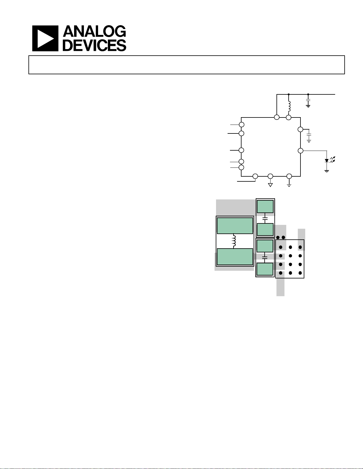
FUNCTIONAL BLOCK DIAGRAM
INPUT VO LTAGE = 2.7V TO 5.0
1.0µH
VIN
LED_OUT
PGND
LED
ANODE
SW
VOUT
PGND
Li-ION +
TX1/TORCH
X2/ILED/ADC
L1
AREA = 16.4mm
GPIO1
GPIO2
ADP1650
STROBE
SCL
SDA
EN SGND
Li-ION +
INDUCTOR
2
Figure 2. PCB Layout (WLCSP)
Figure 1.
1
C
C2
10µF
10µF
MAX 1.5A
DIGITAL
INPUT/
OUTPUT
08837-001
8837-002
GENERAL DESCRIPTION
The ADP1650 is a very compact, highly efficient, single white
LED flash driver for high resolution camera phones that
improves picture and video quality in low light environments.
The device integrates a programmable 1.5 MHz or 3 MHz
synchronous inductive boost converter, an I
2
C-compatible
interface, and a 1500 mA current source. The high switching
frequency enables the use of a tiny, 1 mm high, low cost, 1 µH
power inductor, and the current source permits LED cathode
grounding for thermally enhanced, low EMI, and compact
layouts.
The LED driver maximizes efficiency over the entire battery
voltage range to maximize the input-power-to-LED-power
conversion and to minimize battery current draw during flash
Rev. C
Information furnished by Analog Devices is believed to be accurate and reliable. However, no
responsibility is assumed by Anal og Devices for its use, nor for any infringements of patents or ot her
rights of third parties that may result from its use. Specifications subject to change without notice. No
license is granted by implication or otherwise under any patent or patent rights of Analog Devices.
Trademarks and registered trademarks are the property of their respective owners.
events. A programmable dc battery current limit safely maximizes
LED current for all LED V
and battery voltage conditions.
F
Two independent TxMASK inputs permit the flash LED current
and battery current to reduce quickly during a power amplifier
current burst. The I
2
C-compatible interface enables the programmability of timers, currents, and status bit readback for
operation monitoring and safety control.
The ADP1650 is available in a compact 12-ball, 0.5 mm pitch
WLCSP package and a 10-lead LFCSP package, and operates
within specification over the full −40°C to +125°C junction
temperature range.
One Technology Way, P.O. Box 9106, Norwood, MA 02062-9106, U.S.A.
Tel: 781.329.4700 www.analog.com
Fax: 781.461.3113 ©2010–2011 Analog Devices, Inc. All rights reserved.

ADP1650
TABLE OF CONTENTS
Features.............................................................................................. 1
Applications....................................................................................... 1
Functional Block Diagram .............................................................. 1
General Description ......................................................................... 1
Revision History ............................................................................... 2
Specifications..................................................................................... 3
Recommended Specifications: Input and Output Capacitance
and Inductance ............................................................................. 5
I2C-Compatible Interface Timing Specifications ..................... 5
Absolute Maximum Ratings............................................................ 6
Thermal Data ................................................................................ 6
Thermal Resistance ...................................................................... 6
ESD Caution.................................................................................. 6
Pin Configurations and Function Descriptions ........................... 7
Typical Performance Characteristics ............................................. 8
Theory of Operation ...................................................................... 12
White LED Driver ...................................................................... 12
Modes of Operation ................................................................... 12
Assist Light.................................................................................. 13
Flash Mode .................................................................................. 13
Assist-to-Flash Operation ......................................................... 13
Torch Mode .................................................................................13
Torch-to-Flash Mode................................................................. 14
TxMASK Operation................................................................... 14
Frequency Foldback................................................................... 14
Indicator LED Driver................................................................. 14
Low Battery LED Current Foldback........................................ 14
Programmable Battery DC Current Limit.............................. 15
Analog-to-Digital Converter Operation................................. 15
5 V Output Operation ............................................................... 16
Safety Features................................................................................. 18
Short-Circuit Fault..................................................................... 18
Overvoltage Fault ....................................................................... 18
Dynamic Overvoltage Mode (DOVP) .................................... 18
Timeout Fault.............................................................................. 18
Overtemperature Fault.............................................................. 18
Indicator LED Fault ................................................................... 18
Current Limit.............................................................................. 18
Input Undervoltage.................................................................... 18
Soft Start ...................................................................................... 18
Reset Using the Enable (EN) Pin ............................................. 18
Clearing Faults............................................................................ 18
I2C Interface ................................................................................ 19
I2C Register Map............................................................................. 20
Applications Information.............................................................. 26
External Component Selection ................................................ 26
PCB Layout...................................................................................... 28
Outline Dimensions....................................................................... 29
Ordering Guide .......................................................................... 29
REVISION HISTORY
4/11—Rev. B to Rev. C
Added 10-Lead LFCSP Package........................................Universal
Changes to Features Section, General Description Section, and
Figure 2 Caption ............................................................................... 1
Changes to Table 1............................................................................ 3
Changes to Table 5............................................................................ 6
Added Figure 5; Renumbered Sequentially .................................. 7
Changes to Table 6............................................................................ 7
Changes to PCB Layout Section and Figure 45 Caption........... 28
Added Figure 46.............................................................................. 28
Updated Outline Dimensions....................................................... 29
Changes to Ordering Guide.......................................................... 29
2/11—Rev. A to Rev. B
Changes to Features Section and General Description Section . 1
Changes to Switching Regulator, Voltage Output Mode, VOUT
Voltage Parameter and Digital Inputs/GPIO, Torch Glitch
Filtering Delay Parameter, Table 1.................................................. 3
Rev. C | Page 2 of 32
Changed GND to Power Ground Throughout .............................6
Changed IL to I
IBAT to I
Change to Figure 10 Caption...........................................................8
Change to Figure 11 Caption...........................................................9
Changed LED_MOD = 10 to LED_MOD = 11 in Figure 32 ... 14
Changes to Analog-to-Digital Converter Operation Section and
Figure 37 .......................................................................................... 15
Changes to Selecting the Output Capacitor Section.................. 26
6/10—Rev. 0 to Rev. A
Changes to Contact Information.....................................................1
5/10—Revision 0: Initial Version
, ILED to I
L
Throughout..................................................................8
BAT
, LED OUT to LED_OUT, and
LED

ADP1650
SPECIFICATIONS
1
V
= 3.6 V, TJ = −40°C to +125°C for minimum/maximum specifications, and TA = 25°C for typical specifications, unless otherwise noted.
IN
Table 1.
Parameter2 Conditions Min Typ Max Unit
SUPPLY
Input Voltage Range 2.7 5.0 V
Undervoltage Lockout Threshold VIN falling 2.3 2.4 2.5 V
Undervoltage Lockout Hysteresis 50 100 150 mV
Shutdown Current (IQ), EN = 0 V TJ = −40°C to +85°C, current into VIN pin, VIN = 2.7 V to 4.5 V 0.2 1 μA
Standby Current (I
Operating Quiescent Current Torch mode, LED current = 100 mA 5.3 mA
SW Switch Leakage TJ = −40°C to +85°C, V
T
LED DRIVER
LED Current
Assist Light, Torch Assist light value setting = 0 (000 binary) 25 mA
Assist light value setting = 7 (111 binary) 200 mA
Flash Flash value setting = 0 (00000 binary) 300 mA
Flash value setting = 24 (11000 binary) 1500 mA
LED Current Error—WLCSP I
I
I
I
LED Current Error—LFCSP I
I
I
I
LED Current Source Headroom—WLCSP Flash, 1200 mA LED current 290 mV
Torch, 200 mA LED current 190 mV
LED Current Source Headroom—LFCSP Flash, 1200 mA LED current 370 mV
Torch, 200 mA LED current 220 mV
LED_OUT Ramp-Up Time 0.6 ms
LED_OUT Ramp-Down Time 0.1 ms
SWITCHING REGULATOR
Switching Frequency Switching frequency = 3 MHz 2.8 3 3.2 MHz
Switching frequency = 1.5 MHz 1.4 1.5 1.6 MHz
Minimum Duty Cycle Switching frequency = 3 MHz 14 %
Switching frequency = 1.5 MHz 7 %
nFET Resistance—WLCSP 60 mΩ
pFET Resistance—WLCSP 50 mΩ
nFET Resistance—LFCSP 77 mΩ
pFET Resistance—LFCSP 85 mΩ
Voltage Output Mode
VOUT Voltage—WLCSP 4.575 5.000 5.425 V
VOUT Voltage—LFCSP 4.575 5.000 5.500 V
Output Current 500 mA
Line Regulation I
Load Regulation −0.7 %/A
), EN = 1.8 V TJ = −40°C to +85°C, current into VIN pin, VIN = 2.7 V to 4.5 V 3 10 μA
STBY
3
= 4.5 V 2 μA
= 25°C, V
J
= 700 mA to 1100 mA −6 +6 %
LED
= 300 mA to 650 mA, 1150 mA to 1500 mA −7 +7 %
LED
= 75 mA to 200 mA −10 +10 %
LED
= 25 mA to 50 mA −15 +15 %
LED
= 700 mA to 1100 mA −6 +6 %
LED
= 300 mA to 650 mA, 1150 mA to 1500 mA −7 +7 %
LED
= 75 mA to 200 mA −10 +10 %
LED
= 25 mA to 50 mA −15 +18 %
LED
at VOUT = 300 mA 0.3 %/V
LOAD
3
SW
SW
= 4.5 V 0.5 μA
Rev. C | Page 3 of 32

ADP1650
Parameter2 Conditions Min Typ Max Unit
Pass-Through Mode Transition, Flash
VIN to LED_OUT, Entry 1200 mA LED current 580 mV
VIN to LED_OUT, Exit 1200 mA LED current 435 mV
Pass-Through Mode Transition, Torch
VIN to LED_OUT, Entry 200 mA LED current 380 mV
VIN to LED_OUT, Exit 200 mA LED current 285 mV
DIGITAL INPUTS/GPIO
Input Logic Low Voltage 0.54 V
Input Logic High Voltage 1.26 V
GPIO1, GPIO2, STROBE Pull-Down 390 kΩ
Torch Glitch Filtering Delay From torch rising edge to device start 5.5 7 7.5 ms
INDICATOR LED
LED Current Accuracy −22 +22 %
Short-Circuit Detection Threshold 1.2 V
Open-Circuit Detection Threshold 2.45 V
ADC
Resolution 4 Bits
Error External voltage mode 0 ±1 LSB
V
V
Input Voltage Range, GPIO2 External voltage mode 0 0. 5 V
SAFETY FEATURES
Maximum Timeout For Flash 1600 ms
Timer Accuracy −7.0 +7.0 %
DC Current Limit DC current value setting = 0 (00 binary) 1.35 1.5 1.65 A
DC current value setting = 1 (01 binary) 1.55 1.75 1.95 A
DC current value setting = 2 (10 binary) 1.8 2.0 2.2 A
DC current value setting = 3 (11 binary) 2.02 2.25 2.5 A
Low VBAT Mode Transition Voltage
Error 3.2 %
Hysteresis 50 mV
Coil Peak Current Limit Peak current value setting = 0 (00 binary) 1.55 1.75 1.95 A
Peak current value setting = 1 (01 binary) 2.02 2.25 2.5 A
Peak current value setting = 2 (10 binary) 2.47 2.75 3.0 A
Peak current value setting = 3 (11 binary) 2.7 3.0 3.3 A
Overvoltage Detection Threshold 5.15 5.5 5.9 V
LED_OUT Short-Circuit Detection
Comparator Reference Voltage
Thermal Shutdown Threshold
TJ Rising 150 °C
TJ Falling 140 °C
1
VIN is the input voltage to the circuit.
2
All limits at temperature extremes are guaranteed via correlation using standard statistical quality control (SQC).
3
VSW is the voltage on the SW switch pin.
mode, TJ = 25°C ±1 LSB
F
mode, TJ = −40°C to +125°C ±1.5 LSB
F
1.2 1.3 V
Rev. C | Page 4 of 32
ADP1650
A
RECOMMENDED SPECIFICATIONS: INPUT AND OUTPUT CAPACITANCE AND INDUCTANCE
Table 2.
Parameter Symbol Conditions Min Typ Max Unit
CAPACITANCE C
Input TA = −40°C to +125°C 4.0 10 μF
Output TA = −40°C to +125°C 3.0 10 20 μF
MINIMUM AND MAXIMUM INDUCTANCE L TA = −40°C to +125°C 0.6 1.0 1.5 μH
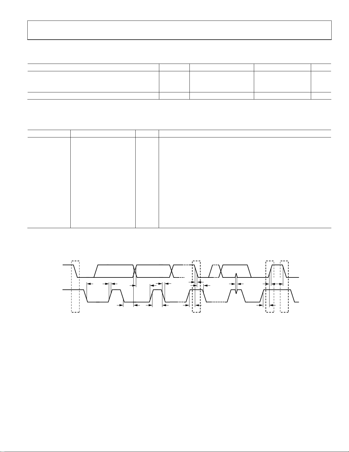
I2C-COMPATIBLE INTERFACE TIMING SPECIFICATIONS
Table 3.
Parameter1 Min Max Unit Description
f
SCL
t
HIGH
t
LOW
t
SU, DAT
t
0 0.9 μs Data hold time
HD, DAT
t
SU, STA
t
HD, STA
t
BUF
t
SU, STO
tR 20 + 0.1 C
tF 20 + 0.1 C
t
SP
2
C
400 pF Capacitive load for each bus line
B
1
Guaranteed by design.
2
CB is the total capacitance of one bus line in picofarads.
400 kHz SCL clock frequency
0.6 μs SCL high time
1.3 μs SCL low time
100 ns Data setup time
0.6 μs Setup time for repeated start
0.6 μs Hold time for start/repeated start
1.3 μs Bus free time between a stop and a start condition
0.6 μs Setup time for stop condition
2
300 ns Rise time of SCL and SDA
B
2
B
300 ns Fall time of SCL and SDA
0 50 ns Pulse width of suppressed spike
MIN
SD
t
LOW
SCL
S
S = START CONDI TION
Sr = REPEATED START CONDITIO N
P = STOP CONDITION
t
R
t
HD, DAT
t
SU, DAT
Figure 3. I
t
F
t
F
t
HIGH
2
C-Compatible Interface Timing Diagram
t
SU, STA
t
HD, STA
Sr P S
Rev. C | Page 5 of 32
t
SP
t
SU, STO
t
BUF
t
R
08837-003
ADP1650
ABSOLUTE MAXIMUM RATINGS
Table 4.
Parameter Rating
VIN, SDA, SCL, EN, GPIO1, GPIO2, STROBE,
LED_OUT, SW, VOUT to Power Ground
PGND to SGND −0.3 V to +0.3 V
Ambient Temperature Range (TA) −40°C to +85°C
Junction Temperature Range (TJ) −40°C to +125°C
Storage Temperature JEDEC J-STD-020
ESD Human Body Model ±2000 V
ESD Charged Device Model ±500 V
ESD Machine Model ±150 V
−0.3 V to +6 V
THERMAL RESISTANCE
θJA of the package is based on modeling and calculation using
a 4-layer board. θ
board layout. In applications where high maximum power dissipation exists, attention to thermal board design is required. The
value of θ
JA
environmental conditions. The specified value of θ
on a 4-layer, 4 in × 3 in, 2 ½ oz copper board, per JEDEC
standards. For more information, see the AN-617 Application
Note, MicroCSP™ Wafer Level Chip Scale Package.
θ
is specified for a device mounted on a JEDEC 2S2P PCB.
JA
is highly dependent on the application and
JA
may vary, depending on PCB material, layout, and
is based
JA
Stresses above those listed under Absolute Maximum Ratings
may cause permanent damage to the device. This is a stress
rating only; functional operation of the device at these or any
other conditions above those indicated in the operational
section of this specification is not implied. Exposure to absolute
maximum rating conditions for extended periods may affect
device reliability.
THERMAL DATA
The ADP1650 may be damaged if the junction temperature
limits are exceeded. Monitoring T
is within the specified temperature limits. In applications with
high power dissipation and poor thermal resistance, the maximum
T
may have to be derated. In applications with moderate power
A
dissipation and low PCB thermal resistance, the maximum T
can exceed the maximum limit as long as the T
fication limits. T
of the device is dependent on the TA, the power
J
dissipation (PD) of the device, and the junction-to-ambient
thermal resistance (θ
calculated from the T
= TA + (PD × θJA)
T
J
) of the package. Maximum TJ is
JA
and PD using the following formula:
A
does not guarantee that TJ
A
is within speci-
J
A
Table 5. Thermal Resistance
Package Type θJA Unit
12-Ball WLCSP 75 °C/W
10-Lead LFCSP 42.5 °C/W
ESD CAUTION
Rev. C | Page 6 of 32
ADP1650
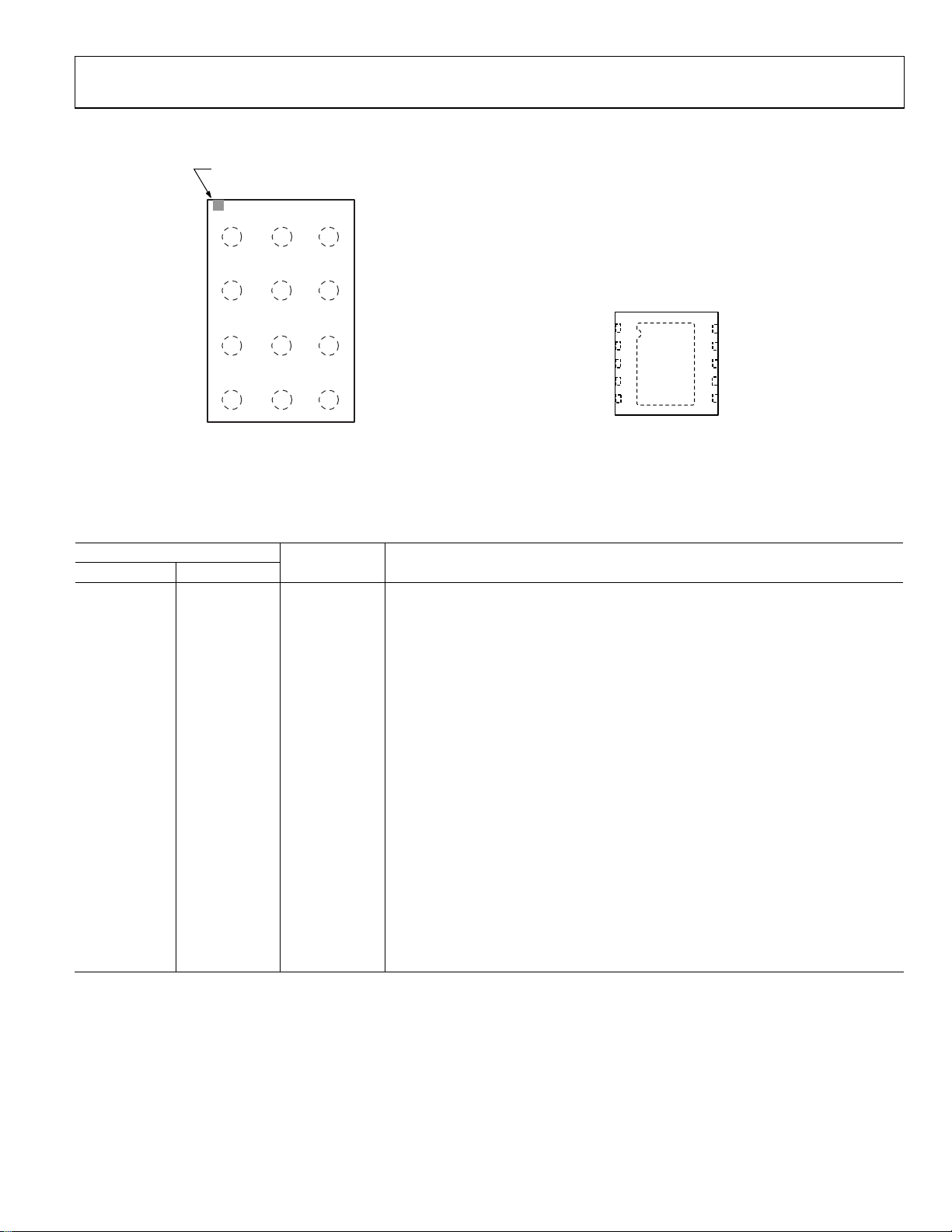
PIN CONFIGURATIONS AND FUNCTION DESCRIPTIONS
BALL A1
INDICATOR
1
PGND SGND VIN
A
23
SW
B
VOUT STROBE EN
C
LED_OUT SDA SCL
D
GPIO2
TOP VIEW
(BALL S IDE DOWN)
Not to Scale
GPIO1
1VIN
2GPIO2
ADP1650
3GPIO1
TOP VIEW
4SDA
5SCL
NOTES
1. THE EXPO SED PADDLE MUS T BE CONNECTED
08837-004
TO GRO UND.
10 STRO BE
9EN
8SW
7VOUT
6LED_OUT
08837-070
Figure 4. WLCSP Pin Configuration Figure 5. LFCSP Pin Configuration
Table 6. Pin Function Descriptions
Pin No.
WLCSP LFCSP Mnemonic Description
A1 N/A1 PGND Power Ground.
A2 N/A1 SGND Signal Ground.
A3 1 VIN Input Voltage for the Device. Connect an input bypass capacitor close to this pin.
B1 8 SW Boost Switch. Connect the power inductor between SW and the input capacitor.
B2 2 GPIO2
ILED/TX2/ADC. Mode is register selectable. Red indicator LED current source or
TxMASK2 or ADC input.
ILED Mode. Connect to red LED anode. Connect the LED cathode to power ground.
TxMASK2 Mode. Reduces the current to the programmable TxMASK2 current.
ADC Mode. This pin is used as the input pin for the ADC.
B3 3 GPIO1
Torch/TX1. Mode is register selectable. External torch mode or TxMASK1 input.
Torch Mode. Enables the integrated circuit (IC) in direct torch mode.
TxMASK1 Mode. Reduces the flash current to the programmable TxMASK1 current.
C1 7 VOUT
Boost Output. Connect an output bypass capacitor very close to this pin. This is the
output for the 5 V external voltage mode.
C2 10 STROBE
Strobe Signal Input. This pin synchronizes the flash pulse to the image capture. In
most cases, this signal comes directly from the image sensor.
C3 9 EN
Enable. Set EN low to bring the quiescent current (I
) to <1 μA. Registers are set to
Q
their defaults when EN is brought from low to high.
D1 6 LED_OUT LED Current Source. Connect this pin to the anode of the flash LED.
D2 4 SDA I2C Data Signal in I2C Mode.
D3 5 SCL I2C Clock Signal in I2C Mode.
0 EPAD Exposed Pad. Connect the exposed pad to the ground plane for the LFCSP version.
1
N/A means not applicable.
Rev. C | Page 7 of 32
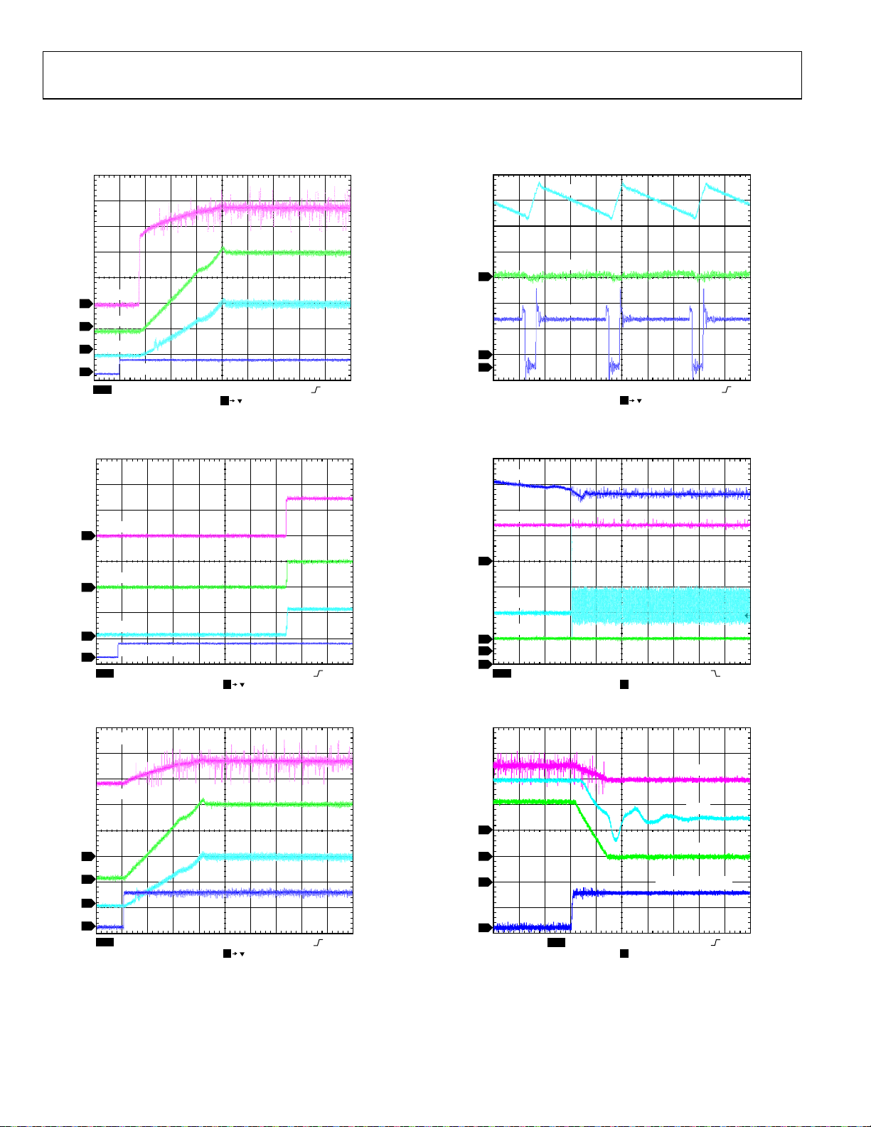
ADP1650
TYPICAL PERFORMANCE CHARACTERISTICS
IL = inductor current, I
LED_OUT
3
I
LED
4
I
L
2
STROBE
1
CH1 5V CH2 1A Ω
Figure 6. Startup Flash Mode, V
= LED current, LED_OUT = LED output, I
LED
CH4 500mA ΩCH3 1V
M100µs A CH1 400mV
T 402.2µs
= 3.6 V, I
IN
= 1500 mA
LED
= battery current.
BAT
I
L
I
4
2
1
08837-025
CH1 2V CH2 100m A Ω
Figure 9. Switching Waveforms, Flash Mode, I
VIN
LED
SW
CH4 25mA Ω
M100ns A CH1 1.6V
T 4.16007ms
= 1500 mA
LED
08837-031
LED_OUT
3
I
LED
4
I
L
2
GPIO1 (Torch)
1
CH1 5V CH2 100mA Ω
CH4 100mA ΩCH3 2V
Figure 7. Startup Torch Mode, V
VIN = 3.6V
LED_OUT
3
I
LED
4
I
L
2
STR
1
CH1 2V CH2 1A Ω
CH4 500mA ΩCH3 1V
M1.00ms A CH1 600mV
T 4.16ms
= 3.6 V, I
IN
M100µs A CH1 440mV
T 394.6µs
Figure 8. 100 mA Torch to 1500 mA Flash Transition
= 100 mA
LED
LED_OUT
3
I
L
I
LED
2
08837-026
08837-028
1
4
CH1 5V CH2 100m A Ω
CH4 100mA ΩCH3 2V
M1ms A CH2 88mA
T 30.40%
Figure 10. Pass-Through to Boost Mode Transition, I
LED_OUT
I
BAT
3
I
4
2
1
CH1 2V
CH2 1A Ω
CH4 500mA ΩCH3 1V
M10µs A CH1 680mV
T 30.60%
LED
GPIO1 (TxMASK1)
= 100 mA
LED
08837-032
08837-035
Figure 11. Entry into TxMASK1 Mode
Rev. C | Page 8 of 32
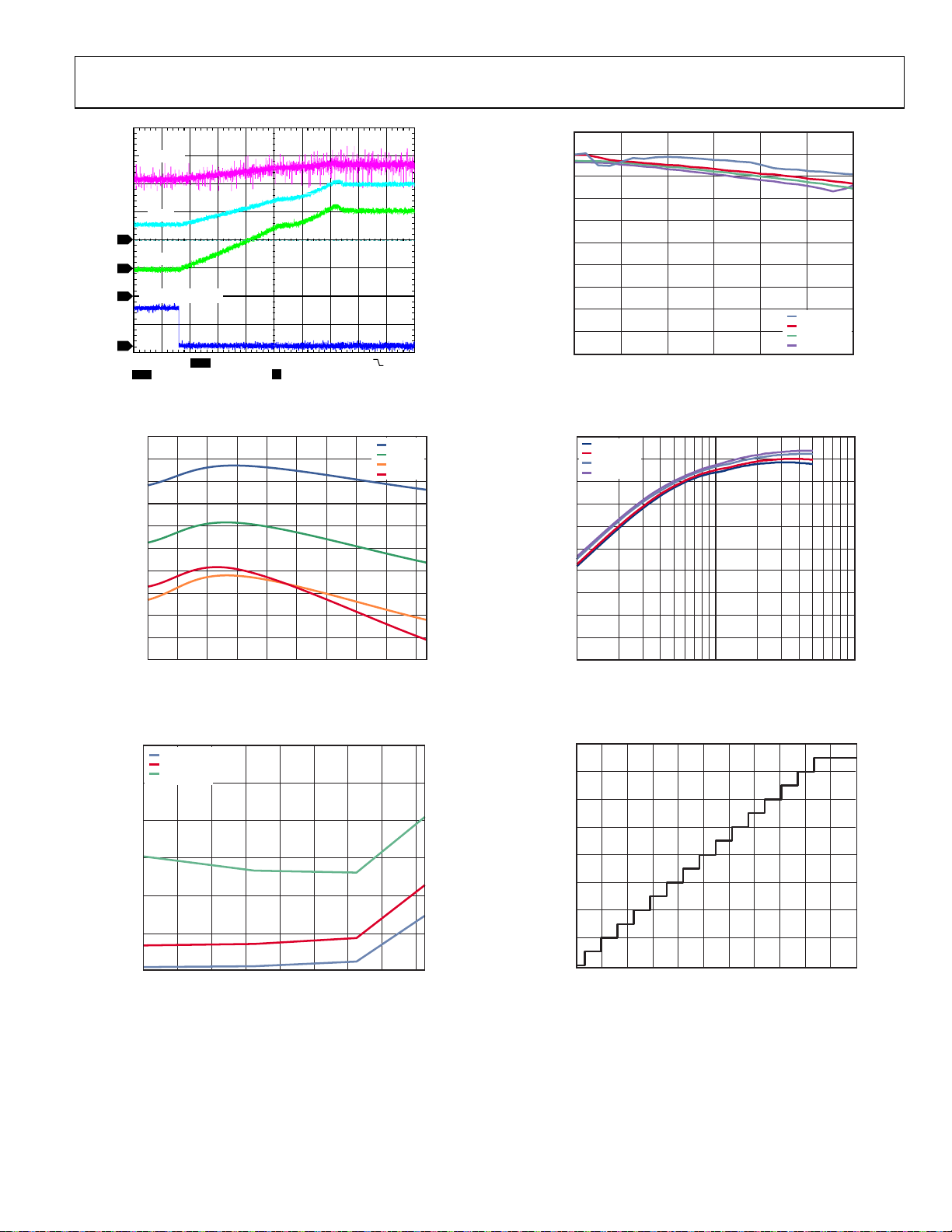
ADP1650
C
C
100
LED_OUT
I
BAT
2
I
LED
3
4
GPIO1 ( TxMASK1)
1
CH2 2V
CH4
1A Ω M40µs A CH1 680mV
CH2
CH4 500mA Ω1V
T 16%
Figure 12. Exit from TxMASK1 Mode
08837-036
90
80
70
60
Y (%)
50
40
EFFICIEN
30
20
10
0
0.30.50.70.91.11.31.5
LED CURRENT (A)
VIN = 4.2V
V
= 3.6V
IN
V
= 3.4V
IN
V
= 3.2V
IN
Figure 15. Flash Mode Efficiency vs. LED Current
8837-044
3.04
3.03
3.02
3.01
3.00
2.99
(MHz)
SW
f
2.98
2.97
2.96
2.95
2.94
2.7 3.0 3.3 3.6 3.9 4.2 4. 5 4.8 5.1 5.4
INPUT VOLTAGE (V)
–40°C
+25°C
+85°C
+125°C
Figure 13. Switching Frequency vs. Supply Voltage (3 MHz Mode)
6
VIN = 2.7V
= 3.6V
V
IN
= 4.5V
V
IN
5
4
3
2
STANDBY CURRENT (µA)
1
100
VIN = 2.7V
= 3.0V
V
IN
90
80
70
60
Y (%)
50
40
EFFICIEN
30
20
10
08837-038
= 3.6V
V
IN
= 4.2V
V
IN
0
0.01 0. 1 1
OUTPUT CURRENT (A)
08837-045
Figure 16. Voltage Regulation Mode Efficiency vs. Load Current
1111
1110
1100
1010
1000
0110
ADC RESULT (Bin ary)
0100
0010
0
–40 –20 0 20 40 60 80 100 120
TEMPERATURE (°C)
Figure 14. Standby Current vs. Temperature
08837-043
0000
0 50 100 150 200 250 300 350 400 450 500 550
ADC INPUT VOLTAGE (mV)
Figure 17. ADC External Voltage Mode Transfer Characteristic
08837-059
Rev. C | Page 9 of 32
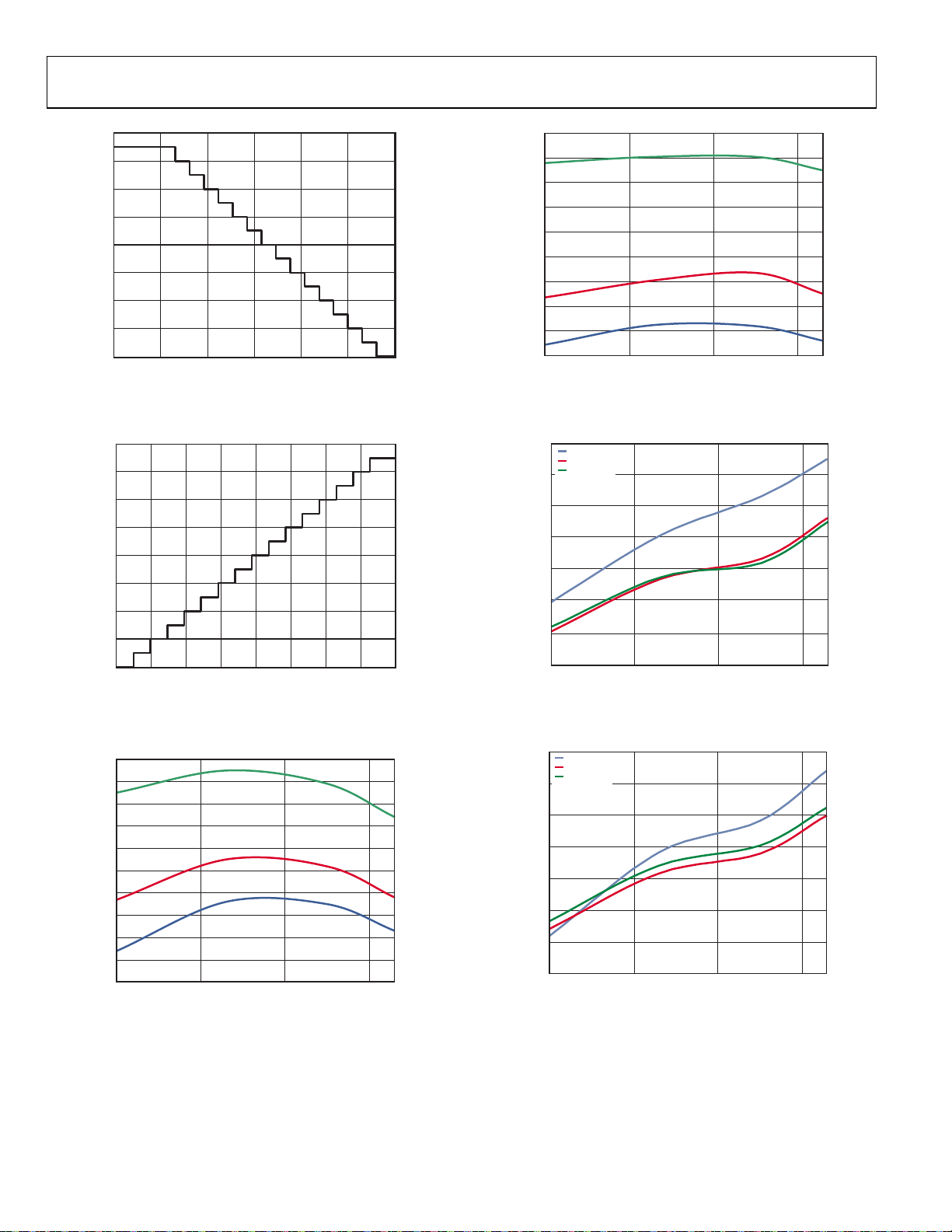
ADP1650
1111
1110
1100
1010
1000
0110
ADC RESULT (Binary)
0100
0010
0000
0 25 50 75 100 125 150
DIE TEMPERATURE (°C)
Figure 18. ADC Die Temperature Mode Transfer Characteristic
08837-060
295
294
293
292
291
290
289
CODE 1000 MIDPOINT (mV)
288
287
286
–40 10 60 110
= 5V
V
IN
V
= 3.6V
IN
V
= 2.7V
IN
TEMPERATURE (°C)
08837-063
Figure 21. ADC External Voltage Mode, Code 1000, Midpoint vs. Temperature
1111
1110
1100
1010
1000
0110
ADC RESULT (Bin ary)
0100
0010
0000
2.8 3.0 3. 2 3. 4 3. 6 3.8 4. 0 4. 2 4. 4
LED_OUT VOLTAGE (V)
Figure 19. ADC LED V
3.760
3.755
3.750
3.745
3.740
3.735
3.730
3.725
CODE 1000 MIDPO INT (V)
3.720
3.715
3.710
–40 10 60 110
Figure 20. ADC LED V
Mode Transfer Characteristic
F
V
= 5.0V
IN
V
IN
VIN = 2.7V
TEMPERATURE (°C)
Mode, Code 1000, Midpoint vs. Temperature
F
= 3.6V
1.0
VIN = 3.2V
V
= 3.6V
IN
V
= 4.2V
IN
0.5
0
–0.5
–1.0
–1.5
LED CURRENT ERROR (%)
LED CURRENT ERROR (%)
–2.0
–2.5
–40 10 60 110
8837-061
Figure 22. LED Current Accuracy vs. Temperature, I
0.5
VIN = 3.2V
V
= 3.6V
IN
V
= 4.2V
IN
0
–0.5
–1.0
–1.5
–2.0
LED CURRENT ERROR (%)
–2.5
–3.0
–40 10 60 110
08837-062
TEMPERATURE (°C)
TEMPERATURE (°C)
= 1200 mA
LED
08837-066
08837-067
Figure 23. LED Current Accuracy vs. Temperature, I
= 800 mA
LED
Rev. C | Page 10 of 32
 Loading...