

650 kHz /1.3 MHz Step-Up
ADP1612/ADP1613
ADP1612/
ADP1613
6
3
7
8
5
2
1
4
VIN
EN
FREQ
SS
SW
FB
COMP
GND
ON
OFF
1.3MHz
650kHz
(DEFAULT)
V
OUT
V
IN
L1
C
IN
C
SS
C
OUT
C
COMP
R
COMP
R1
R2
D1
06772-001
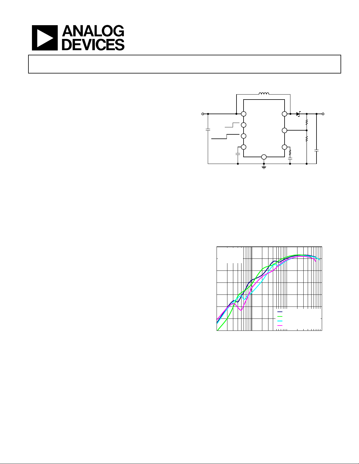
100
90
80
70
60
50
40
30
1 10 100 1k
LOAD CURRENT ( mA)
EFFICIENCY (%)
06772-009
VIN = 5V
f
SW
= 1.3MHz
T
A
= 25°C
ADP1612, V
OUT
= 12V
ADP1612, V
OUT
= 15V
ADP1613, V
OUT
= 12V
ADP1613, V
OUT
= 15V
PWM DC-to-DC Switching Converters
FEATURES
Current limit
1.4 A for the ADP1612
2.0 A for the ADP 1613
Minimum input voltage
1.8 V for the ADP1612
2.5 V for the ADP1613
Pin-selectable 650 kHz or 1.3 MHz PWM frequency
Adjustable output voltage up to 20 V
Adjustable soft start
Undervoltage lockout
Thermal shutdown
8-lead MSOP
ADIsimPower™ online design tool
ADIsimPower downloadable design tools for boost, coupled-
SEPIC, and SEPIC Cuk configurations
APPLICATIONS
TFT LCD bias supplies
Portable applications
Industrial/instrumentation equipment
TYPICAL APPLICATION CIRCUIT
Figure 1. Step-Up Regulator Configuration
GENERAL DESCRIPTION
The ADP1612/ADP1613 are step-up dc-to-dc switching converters with an integrated power switch capable of providing
an output voltage as high as 20 V. With a package height of less
than 1.1 mm, the ADP1612/ADP1613 are optimal for spaceconstrained applications such as portable devices or thin film
transistor (TFT) liquid crystal displays (LCDs).
The ADP1612/ADP1613 operate in current mode pulse-width
modulation (PWM) with up to 94% efficiency. Adjustable
soft start prevents inrush currents when the part is enabled.
The pin-selectable switching frequency and PWM current-mode
architecture allow for excellent transient response, easy noise
filtering, and the use of small, cost-saving external inductors
and capacitors. Other key features include undervoltage lockout
(UVLO), thermal shutdown (TSD), and logic controlled enable.
The ADP1612/ADP1613 are available in the lead-free
8-lead MSOP.
Rev. B
Information furnished by Analog Devices is believed to be accurate and reliable. However, no
responsibility is assumed by Analog Devices for its use, nor for any infringements of patents or other
rights of third parties that may result from its use. Specifications subject to change without notice. No
license is granted by implication or otherwise under any patent or patent rights of Analog Devices.
Trademarks and registered trademarks are the property of their respective owners.
Figure 2. ADP1612/ADP1613 Efficiency for Various Output Voltages
One Technology Way, P.O. Box 9106, Norwood, MA 02062-9106, U.S.A.
Tel: 781.329.4700
Fax: 781.461.3113 ©2009–2011 Analog Devices, Inc. All rights reserved.
www.analog.com
 Loading...