

Analog Devices ADP1611 Datasheet
20 V,1.2 MHz Step-Up
FEATURES
Fully integrated 1.2 A , 0.23 Ω power switch
Pin-selectable 700 kHz or 1.2 MHz PWM frequency
90% efficiency
Adjustable output voltage up to 20 V
3% output regulation accuracy
Adjustable soft start
Input undervoltage lockout
MSOP 8-lead package
APPLICATIONS
TFT LC bias supplies
Portable applications
Industrial/instrumentation equipment
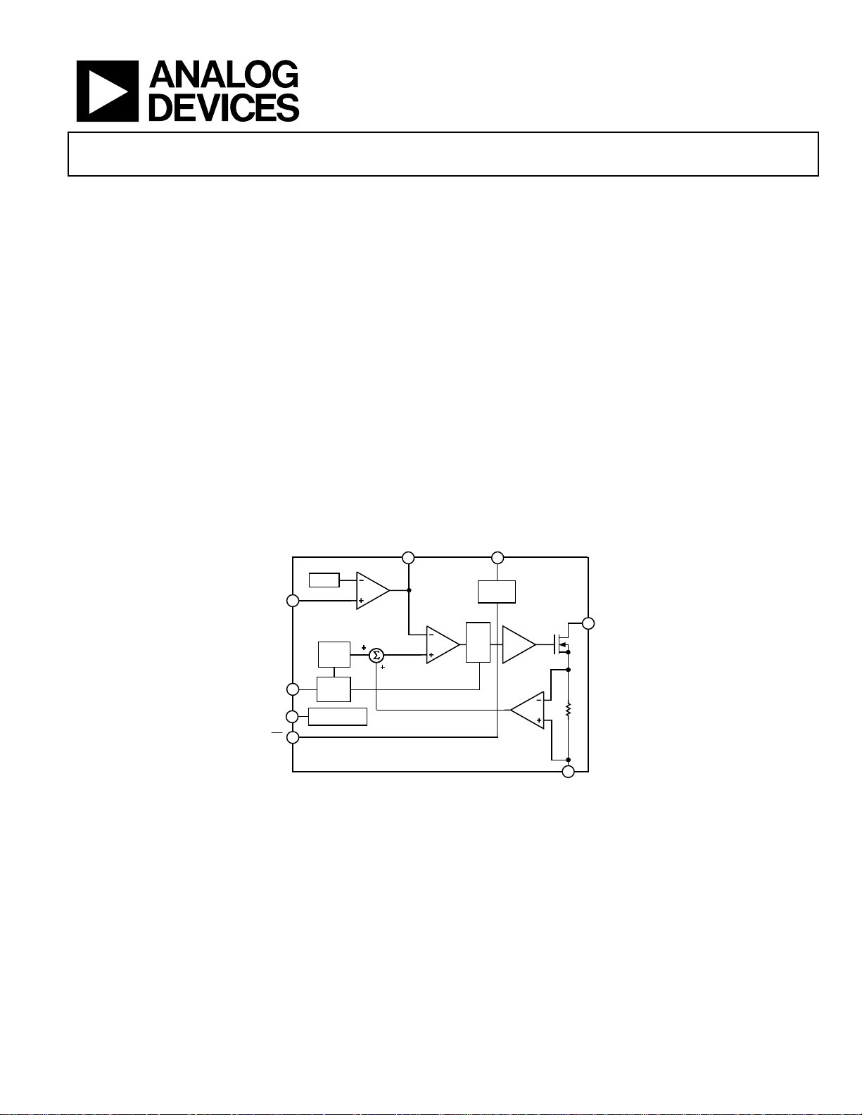
FUNCTIONAL BLOCK DIAGRAM
REF
FB
2
RAMP
GEN
7
RT
OSC
ERROR
g
m
COMP
1 6
AMP
COMPARATOR
DC-to-DC Switching Converter
ADP1611
GENERAL DESCRIPTION
The ADP1611 is a step-up dc-to-dc switching converter with an
integrated 1.2 A, 0.23 Ω power switch capable of providing an
output voltage as high as 20 V. With a package height of less
than 1.1 mm, the ADP1611 is optimal for space-constrained
applications such as portable devices or thin film transistor
(TFT) liquid crystal displays (LCDs).
The ADP1611 operates in pulse-width modulation (PWM)
current mode with up to 90% efficiency. Adjustable soft start
prevents inrush currents at startup. The pin-selectable switching
frequency and PWM current-mode architecture allow excellent
transient response, easy noise filtering, and the use of small,
cost-saving external inductors and capacitors.
The ADP1611 is offered in the Pb-free 8-lead MSOP and
operates over the temperature range of −40°C to +85°C.
IN
ADP1611
BIAS
SW
F/F
QSR
DRIVER
5
8
SOFT START
SS
3
SD
Rev. 0
Information furnished by Analog Devices is believed to be accurate and reliable.
However, no responsibility is assumed by Analog Devices for its use, nor for any
infringements of patents or other rights of third parties that may result from its use.
Specifications subject to change without notice. No license is granted by implication
or otherwise under any patent or patent rights of Analog Devices. Trademarks and
registered trademarks are the property of their respective owners.
Figure 1.
CURRENT-
SENSE
AMPLIFIER
4
GND
One Technology Way, P.O. Box 9106, Norwood, MA 02062-9106, U.S.A.
Tel: 781.329.4700
Fax: 781.326.8703 © 2005 Analog Devices, Inc. All rights reserved.
www.analog.com
04906-001

ADP1611
TABLE OF CONTENTS
Specifications..................................................................................... 3
Choosing the Input and Output Capacitors ........................... 11
Absolute Maximum Ratings............................................................ 4
ESD Caution.................................................................................. 4
Pin Configuration and Function Descriptions............................. 5
Typical Performance Characteristics ............................................. 6
Theory of Operation ...................................................................... 10
Current-Mode PWM Operation.............................................. 10
Frequency Selection ................................................................... 10
Soft Start ......................................................................................10
On/Off Control........................................................................... 10
Setting the Output Voltage........................................................ 10
REVISION HISTORY
2/05—Revision 0: Initial Version
Diode Selection........................................................................... 12
Loop Compensation .................................................................. 12
Soft-Start Capacitor ................................................................... 13
Application Circuits ................................................................... 14
Step-Up DC-to-DC Converter with True Shutdown............ 14
TFT LCD Bias Supply ................................................................ 14
SEPIC Power Supply .................................................................. 15
Layout Procedure ........................................................................... 16
Outline Dimensions ....................................................................... 18
Ordering Guide .......................................................................... 18
Rev. 0 | Page 2 of 20

ADP1611
SPECIFICATIONS
VIN = 3.3 V, TA = −40°C to +85°C, unless otherwise noted. All limits at temperature extremes are guaranteed by correlation and
characterization using standard statistical quality control (SQC), unless otherwise noted.
Table 1.
Parameter Symbol Conditions Min Typ Max Unit
SUPPLY
Input Voltage V
IN
Quiescent Current
Nonswitching State I
Shutdown I
Switching State
1
Q
SD
Q
IQ
SW
OUTPUT
Output Voltage V
OUT
Load Regulation I
Overall Regulation Line, load, temperature ±3 %
REFERENCE
Feedback Voltage V
FB
Line Regulation VIN = 2.5 V to 5.5 V −0.15 +0.15 %/V
ERROR AMPLIFIER
Transconductance g
Voltage Gain A
m
V
FB Input Bias Current V
SWITCH
SW On Resistance R
ON
SW Leakage Current VSW = 20 V 0.01 20 µA
Peak Current Limit
2
I
CLSET
OSCILLATOR
Oscillator Frequency f
RT = GND 0.49 0.7 0.885 MHz
OSC
RT = IN 0.89 1.23 1.6 MHz
Maximum Duty Cycle D
MAX
SHUTDOWN
Shutdown Input Voltage Low V
Shutdown Input Voltage High V
Shutdown Input Bias Current I
IL
IH
SD
SOFT START
SS Charging Current VSS = 0 V 3 µA
UNDERVOLTAGE LOCKOUT
3
UVLO Threshold VIN rising 2.2 2.4 2.5 V
UVLO Hysteresis 220 mV
1
This parameter specifies the average current while switching internally and with SW (Pin 5) floating.
2
Guaranteed by design and not fully production tested.
3
Guaranteed by characterization.
2.5 5.5 V
VFB = 1.3 V, RT = V
IN
390 600 µA
VSD = 0 V 0.01 10 µA
fSW = 1.23 MHz, no load 1 2 mA
V
= 10 mA to 150 mA, V
LOAD
= 10 V 0.05 mV/mA
OUT
IN
20 V
1.212 1.230 1.248 V
∆I = 1 µA
100 µA/V
60 dB
= 1.23 V
FB
10 nA
ISW = 1.0 A 230 600 mΩ
2.0 A
COMP = open, VFB = 1 V, RT = GND 78 83 90 %
0.6 V
2.2 V
VSD = 3.3 V 0.01 1 µA
Rev. 0 | Page 3 of 20
ADP1611
7
ABSOLUTE MAXIMUM RATINGS
Table 2.
Parameter Rating
IN, COMP, SD, SS, RT, FB to GND
SW to GND 22 V
RMS SW Pin Current 1.2 A
Operating Ambient Temperature Range −40°C to +85°C
Operating Junction Temperature Range −40°C to +125°C
Storage Temperature Range −65°C to +150°C
θJA, Two Layers 206°C/W
θJA, Four Layers 142°C/W
Lead Temperature Range (Soldering, 60 sec) 300°C
−0.3 V to +6 V
Stresses above those listed under Absolute Maximum Ratings
may cause permanent damage to the device. This is a stress
rating only; functional operation of the device at these or any
other conditions above those indicated in the operational
section of this specification is not implied. Exposure to absolute
maximum rating conditions for extended periods may affect
device reliability. Absolute maximum ratings apply individually
only, not in combination. Unless otherwise specified, all other
voltages are referenced to GND.
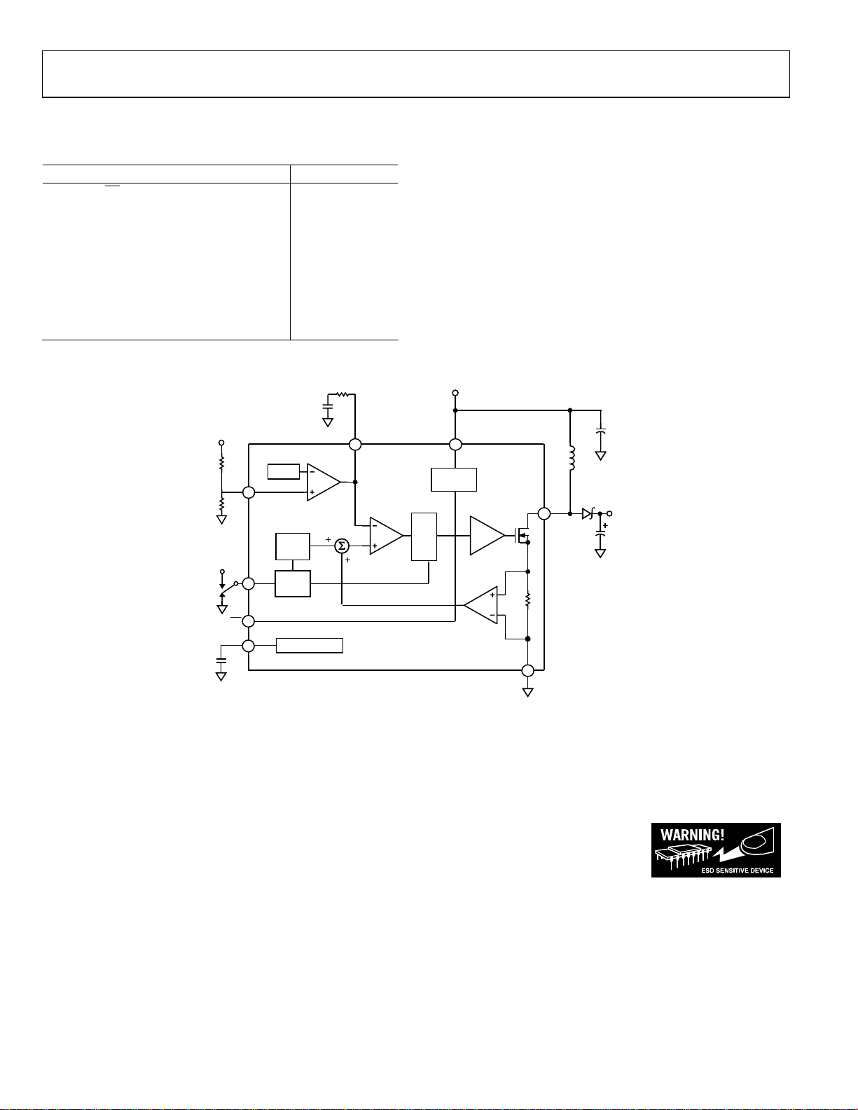
F/F
QSR
IN
IN
BIAS
CURRENT-
SENSE
AMPLIFIER
ADP1611
DRIVER
C
IN
L1
D1
SW
5
4
GND
V
OUT
C
OUT
04906-002
R1
1.2MHz
00kHz
C
SS
R
C
C
C
V
OUT
FB
R2
V
IN
SD
SS
REF
2
RAMP
GEN
RT
7
OSC
3
SOFT START
8
COMP
1 6
ERROR
AMP
g
m
COMPARATOR
Figure 2. Block Diagram and Typical Application Circuit
ESD CAUTION
ESD (electrostatic discharge) sensitive device. Electrostatic charges as high as 4000 V readily accumulate on
the human body and test equipment and can discharge without detection. Although this product features
proprietary ESD protection circuitry, permanent damage may occur on devices subjected to high energy
electrostatic discharges. Therefore, proper ESD precautions are recommended to avoid performance
degradation or loss of functionality.
Rev. 0 | Page 4 of 20

ADP1611
PIN CONFIGURATION AND FUNCTION DESCRIPTIONS
COMP
FB
SD
GND
1
ADP1611
2
TOP VIEW
3
(Not to Scale)
4
8
SS
RT
7
6
IN
SW
5
04906-0-003
Figure 3. Pin Configuration
Table 3. Pin Function Descriptions
Pin No. Mnemonic Description
1 COMP
Compensation Input. Connect a series resistor-capacitor network from COMP to GND to compensate the
regulator.
2 FB
Output Voltage Feedback Input. Connect a resistive voltage divider from the output voltage to FB to set the
regulator output voltage.
3
SD Shutdown Input. Drive SD low to shut down the regulator; drive SD high to turn it on.
4 GND Ground.
5 SW
Switching Output. Connect the power inductor from the input voltage to SW and connect the external rectifier
from SW to the output voltage to complete the step-up converter.
6 IN
Main Power Supply Input. IN powers the ADP1611 internal circuitry. Connect IN to the input source voltage.
Bypass IN to GND with a 10 µF or greater capacitor as close to the ADP1611 as possible.
7 RT
Frequency Setting Input. RT controls the switching frequency. Connect RT to GND to program the oscillator to
700 kHz, or connect RT to IN to program it to 1.2 MHz.
8 SS Soft-Start Timing Capacitor Input. A capacitor from SS to GND brings up the output slowly at power-up.
Rev. 0 | Page 5 of 20
ADP1611
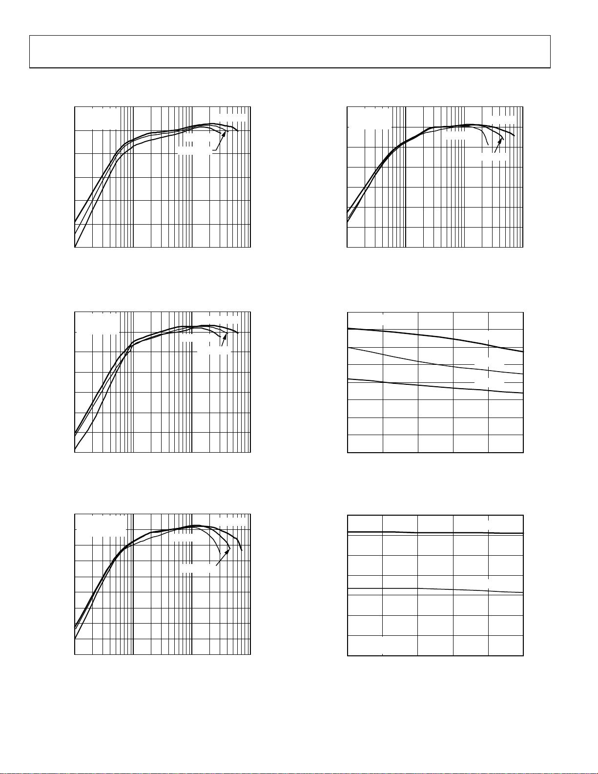
TYPICAL PERFORMANCE CHARACTERISTICS
100
EFFICIENCY (%)
90
80
70
60
VIN = 5V
F
= 700kHz
SW
L = 10µH
V
OUT
V
OUT
= 15V
= 20V
V
= 10V
OUT
EFFICIENCY (%)
100
90
80
70
60
50
VIN = 3.3V
F
= 1.2MHz
SW
L = 4.7µH
V
= 5V
OUT
V
= 13V
OUT
V
= 8.5V
OUT
50
40
1 10 100 1000
LOAD CURRENT (mA)
Figure 4. Output Efficiency vs. Load Current
100
VIN = 5V
= 1.2MHz
F
SW
L = 6.8µH
90
80
70
60
EFFICIENCY (%)
50
40
30
1 10 100 1000
LOAD CURRENT (mA)
V
V
= 20V
OUT
V
OUT
Figure 5. Output Efficiency vs. Load Current
OUT
= 15V
= 10V
04906-004
04906-005
40
30
1 10 100 1000
LOAD CURRENT (mA)
Figure 7. Output Efficiency vs. Load Current
2.8
V
= 10V
OUT
2.6
2.4
2.2
2.0
1.8
CURRENT LIMIT (A)
1.6
1.4
1.2
–40 –15 10 35 60 85
AMBIENT TEMPERATURE (°C)
= 5.5V
V
IN
V
IN
VIN = 2.5V
Figure 8. Current Limit vs. Ambient Temperature, V
= 3.3V
OUT
04906-007
04906-008
= 10 V
95
VIN = 3.3V
= 700kHz
F
SW
90
L = 10µH
85
80
75
70
EFFICIENCY (%)
65
60
55
50
1 10 100 1000
LOAD CURRENT (mA)
V
= 13V
OUT
V
= 8.5V
OUT
Figure 6. Output Efficiency vs. Load Current
V
= 5V
OUT
04906-006
1.4
1.2
1.0
0.8
0.6
0.4
OSCILLATORY FREQUENCY (MHz)
0.2
V
= 10V
OUT
= 3.3V
V
IN
0
–40 –15 10 35 60 85
AMBIENT TEMPERATURE (°C)
RT = V
RT = GND
IN
04906-009
Figure 9. Oscillatory Frequency vs. Ambient Temperature
Rev. 0 | Page 6 of 20
 Loading...