

1.2 MHz DC-to-DC Step-Up Switching
S
www.BDTIC.com/ADI
FEATURES
Fully integrated 1.2 A, 0.2 Ω, power switch
Pin-selectable 700 kHz or 1.2 MHz PWM frequency
92% efficiency
Adjustable output voltage up to 12 V
3% output regulation accuracy
Adjustable soft start
Input undervoltage lockout
MSOP 8-lead package
APPLICATIONS
TFT LC bias supplies
Portable applications
Industrial/instrumentation equipment
FUNCTIONAL BLOCK DIAGRAM
REF
FB
2
RAMP
GEN
7
RT
OSC
ERROR
g
m
COMP
1 6
AMP
COMPARATOR
Converter
ADP1610
GENERAL DESCRIPTION
The ADP1610 is a dc-to-dc step-up switching converter with
an integrated 1.2 A, 0.2 power switch capable of providing
an output voltage as high as 12 V. With a package height of less
than 1.1 mm, the ADP1610 is optimal for space-constrained
applications such as portable devices or thin film transistor
(TFT) liquid crystal displays (LCDs).
The ADP1610 operates in pulse-width modulation (PWM) current
mode with up to 92% efficiency. Adjustable soft start prevents
inrush currents at startup. The pin-selectable switching frequency
and PWM current mode architecture allow excellent transient
response, easy noise filtering, and the use of small, cost-saving
external inductors and capacitors.
The ADP1610 is offered in the RoHS compliant 8-lead MSOP
and operates over the temperature range of −40°C to +85°C.
IN
ADP1610
BIAS
SW
F/F
QSR
DRIVER
5
8
SOFT START
SS
3
D
Rev. A
Information furnished by Analog Devices is believed to be accurate and reliable. However, no
responsibility is assumed by Analog Devices for its use, nor for any infringements of patents or other
rights of third parties that may result from its use. Specifications subject to change without notice. No
license is granted by implication or otherwise under any patent or patent rights of Analog Devices.
Trademarks and registered trademarks are the property of their respective owners.
CURRENT
SENSE
AMPLIFIER
4
Figure 1.
One Technology Way, P.O. Box 9106, Norwood, MA 02062-9106, U.S.A.
Tel: 781.329.4700 www.analog.com
Fax: 781.461.3113 ©2004–2008 Analog Devices, Inc. All rights reserved.
GND
04472-001

ADP1610
www.BDTIC.com/ADI
TABLE OF CONTENTS
Features .............................................................................................. 1
Applications ....................................................................................... 1
General Description ......................................................................... 1
Functional Block Diagram .............................................................. 1
Revision History ............................................................................... 2
Specifications ..................................................................................... 3
Absolute Maximum Ratings ............................................................ 4
ESD Caution .................................................................................. 4
Pin Configuration and Function Descriptions ............................. 5
Typical Performance Characteristics ............................................. 6
Theory of Operation ...................................................................... 10
Current Mode PWM Operation ............................................... 10
Frequency Selection ................................................................... 10
Soft Start ...................................................................................... 10
On/Off Control ........................................................................... 10
Setting the Output Voltage ........................................................ 10
Inductor Selection ...................................................................... 10
Choosing the Input and Output Capacitors ........................... 11
Diode Selection ........................................................................... 13
Loop Compensation .................................................................. 13
Soft Start Capacitor .................................................................... 14
Application Circuits ................................................................... 15
DC-to-DC Step-Up Switching Converter with True
Shutdown ..................................................................................... 15
TFT LCD Bias Supply ................................................................ 15
Sepic Power Supply .................................................................... 16
Layout Procedure ........................................................................... 17
Outline Dimensions ....................................................................... 18
Ordering Guide .......................................................................... 18
REVISION HISTORY
9/08—Rev. 0 to Rev. A
Changes to Table 4 .......................................................................... 11
Changes to Table 5 .......................................................................... 14
10/04—Revision 0: Initial Version
Rev. A | Page 2 of 20
ADP1610
www.BDTIC.com/ADI
SPECIFICATIONS
VIN = 3.3 V, TA = −40°C to +85°C, unless otherwise noted. All limits at temperature extremes are guaranteed by correlation and
characterization using standard statistical quality control (SQC), unless otherwise noted.
Table 1.
Parameter Symbol Conditions Min Typ Max Unit
SUPPLY
Input Voltage VIN 2.5 5.5 V
Quiescent Current
Nonswitching State IQ V
Shutdown I
Switching State
1
V
SD
Q
I
F
QSW
OUTPUT
Output Voltage V
V
OUT
Load Regulation I
Overall Regulation Line, load, temperature ±3 %
REFERENCE
Feedback Voltage VFB 1.212 1.230 1.248 V
Line Regulation VIN = 2.5 V to 5.5 V −0.15 +0.15 %/V
ERROR AMPLIFIER
Transconductance gm ∆I = 1 A 100 µA/V
Voltage Gain AV 60 dB
FB Input Bias Current VFB= 1.23 V 10 nA
SWITCH
SW On Resistance RON I
SW Leakage Current VSW = 12 V 0.01 20 µA
Peak Current Limit
2
I
2.0 A
CLSET
OSCILLATOR
Oscillator Frequency f
RT = GND 0.49 0.7 0.885 MHz
OSC
RT = IN 0.89 1.23 1.6 MHz
Maximum Duty Cycle D
COMP = open, VFB = 1 V, RT = GND 78 83 90 %
MAX
SHUTDOWN
Shutdown Input Voltage Low VIL Nonswitching state 0.6 V
Shutdown Input Voltage High VIH Switching state 2.2 V
Shutdown Input Bias Current I
SD
SOFT START
SS Charging Current VSS = 0 V 3 µA
UNDERVOLTAGE LOCKOUT
3
UVLO Threshold VIN rising 2.2 2.4 2.5 V
UVLO Hysteresis 220 mV
1
This parameter specifies the average current while switching internally and with SW (Pin 5) floating.
2
Guaranteed by design and not fully production tested.
3
Guaranteed by characterization.
= 1.3 V, RT = VIN 390 600 A
FB
= 0 V 0.01 10 µA
SD
= 1.23 MHz, no load 1 2 mA
SW
12 V
IN
= 10 mA to 150 mA, V
LOAD
= 1.0 A 200 400 mΩ
SW
= 10 V 0.05 mV/mA
OUT
VSD = 3.3 V 0.01 1 µA
Rev. A | Page 3 of 20
ADP1610
7
www.BDTIC.com/ADI
ABSOLUTE MAXIMUM RATINGS
Table 2.
Parameter Rating
IN, COMP, SD, SS, RT, FB to GND
−0.3 V to +6 V
SW to GND 14 V
RMS SW Pin Current 1.2 A
Operating Ambient Temperature Range −40°C to +85°C
Operating Junction Temperature Range −40°C to +125°C
Storage Temperature Range −65°C to +150°C
θJA, Two Layers 206°C/W
θJA, Four Layers 142°C/W
Lead Temperature (Soldering, 60 sec) 300°C
Stresses above those listed under Absolute Maximum Ratings
may cause permanent damage to the device. This is a stress
rating only; functional operation of the device at these or any
other conditions above those indicated in the operational
section of this specification is not implied. Exposure to absolute
maximum rating conditions for extended periods may affect
device reliability.
R
C
C
C
V
R1
1.2MHz
00kHz
C
SS
OUT
FB
R2
V
IN
SD
SS
REF
2
RAMP
GEN
RT
7
OSC
3
SOFT START
8
COMP
1 6
ERROR
AMP
g
m
COMPARATOR
Figure 2. Block Diagram and Typical Application Circuit
ESD CAUTION
IN
IN
ADP1610
BIAS
F/F
QSR
DRIVER
CURRENT
SENSE
AMPLIFIER
C
IN
L1
D1
SW
5
4
GND
V
OUT
C
OUT
04472-002
Rev. A | Page 4 of 20
ADP1610
www.BDTIC.com/ADI
PIN CONFIGURATION AND FUNCTION DESCRIPTIONS
1
COMP
GND
ADP1610
FB
2
TOP VIEW
SD
3
(Not to Scale)
4
Figure 3. Pin Configuration
8
SS
RT
7
IN
6
SW
5
04472-003
Table 3. Pin Function Descriptions
Pin No. Mnemonic Description
1 COMP
Compensation Input. Connect a series resistor-capacitor network from COMP to GND to compensate the
regulator.
2 FB
Output Voltage Feedback Input. Connect a resistive voltage divider from the output voltage to FB to set the
regulator output voltage.
3
Shutdown Input. Drive SD low to shut down the regulator; drive SD high to turn it on.
SD
4 GND Ground.
5 SW
Switching Output. Connect the power inductor from the input voltage to SW and connect the external rectifier
from SW to the output voltage to complete the step-up converter.
6 IN
Main Power Supply Input. IN powers the ADP1610 internal circuitry. Connect IN to the input source voltage.
Bypass IN to GND with a 10 µF or greater capacitor as close to the ADP1610 as possible.
7 RT
Frequency Setting Input. RT controls the switching frequency. Connect RT to GND to program the oscillator to 700 kHz,
or connect RT to IN to program the oscillator to 1.2 MHz.
8 SS Soft Start Timing Capacitor Input. A capacitor from SS to GND brings up the output slowly at power-up.
Rev. A | Page 5 of 20
ADP1610
www.BDTIC.com/ADI
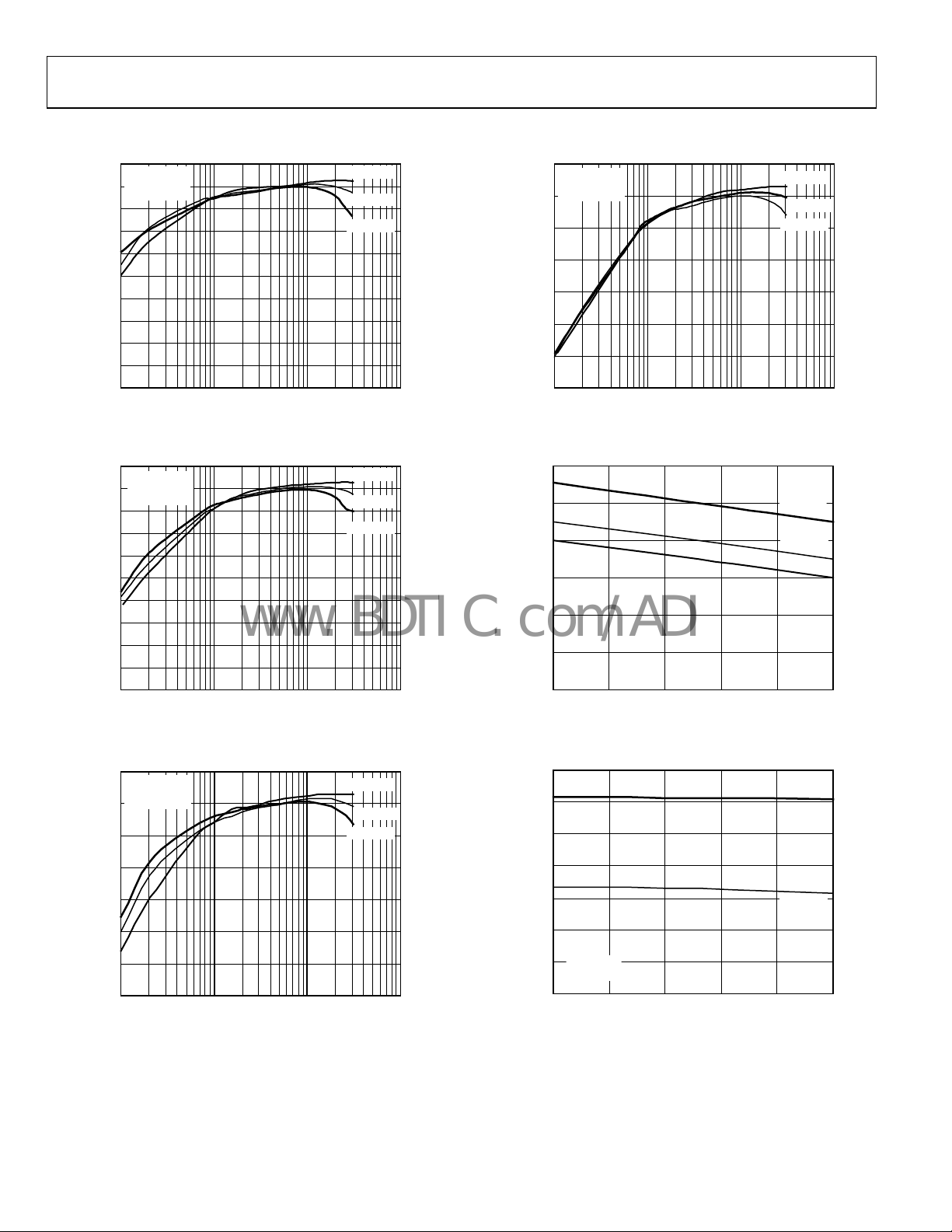
TYPICAL PERFORMANCE CHARACTERISTICS
100
V
= 10V
OUT
F
= 700kHz
SW
90
L = 10µH
80
70
60
50
40
EFFICIENCY (%)
30
20
10
0
110100
LOAD CURRENT (mA)
Figure 4. Output Efficiency vs. Load Current
VIN = 5.5V
VIN = 3.3V
VIN = 2.5V
04472-005
1k
100
V
= 7.5V
OUT
F
= 1.2MHz
SW
L = 4.7µH
90
80
70
60
EFFICIENCY (%)
50
40
30
110100
LOAD CURRENT (mA)
Figure 7. Output Efficiency vs. Load Current
VIN = 5.5V
VIN = 3.3V
VIN = 2.5V
04472-008
1k
100
V
= 10V
OUT
F
= 1.2MHz
90
SW
L = 4.7µH
80
70
60
50
40
EFFICIENCY (%)
30
20
10
0
1 10 100 1K
LOAD CURRENT (mA)
Figure 5. Output Efficiency vs. Load Current
100
V
= 7.5V
OUT
F
= 700kHz
SW
90
L = 10µH
80
70
60
EFFICIENCY (%)
50
40
30
110100
LOAD CURRENT (mA)
Figure 6. Output Efficiency vs. Load Current
VIN = 5.5V
VIN = 3.3V
VIN = 2.5V
VIN = 5.5V
VIN = 3.3V
VIN = 2.5V
04472-006
04472-007
1k
2.4
2.2
2.0
1.8
1.6
CURRENT LIMIT (A)
1.4
1.2
–40 –15 10 35 60 85
AMBIENT TEMPERATURE (°C)
Figure 8. Current Limit vs. Ambient Temperature, V
1.4
1.2
1.0
0.8
0.6
0.4
OSCILLATORY FREQUENCY (MHz)
V
0.2
0
–40 –15 10 35 60 85
= 10V
OUT
V
= 3.3V
IN
AMBIENT TEMPERATURE (°C)
Figure 9. Oscillatory Frequency vs. Ambient Temperature
V
= 5.5V
IN
V
= 3.3V
IN
VIN = 2.5V
= 10 V
OUT
RT = V
RT = GND
04472-009
IN
04472-010
Rev. A | Page 6 of 20

ADP1610
A
R
www.BDTIC.com/ADI
1.4
1.2
1.0
0.8
Y FREQUENCY (MHz)
0.6
TO
0.4
OSCILL
0.2
V
= 10V
OUT
0
2.5 3.0 3.5 4.0 4.5 5.0 5.5
SUPPLY VOLTAGE (V)
Figure 10. Oscillatory Frequency vs. Supply Voltage
350
300
250
200
150
100
SWITCH RESI STANCE (mΩ)
50
RT = V
RT = GND
= 2.5V
V
IN
V
= 3.3V
IN
VIN = 5.5V
0.50
FSW = 700kHz
V
= 1.3V
FB
IN
04472-011
0.45
0.40
0.35
0.30
QUIESCENT CURRENT (mA)
0.25
0.20
–40 –15 10 35 60 85
AMBIENT TEMPERATURE (°C)
VIN = 5.5V
V
= 3.3V
IN
VIN = 2.5V
04472-014
Figure 13. Quiescent Current vs. Ambient Temperature
0.60
FSW = 1.23kHz
V
= 1.3V
FB
0.55
0.50
0.45
0.40
QUIESCENT CURRENT (mA)
0.35
= 5.5V
V
IN
V
= 3.3V
IN
VIN = 2.5V
0
–40 –15 10 35 60 85
AMBIENT TEMPERATURE (°C)
Figure 11. Switch Resistance vs. Ambient Temperature
1.245
1.24
1.235
1.23
1.225
1.22
FB REGULATION VOLTAGE (V)
1.215
1.21
–40 –10–25 2055035 80 95 11065 125
AMBIENT TEMPERATURE (°C)
Figure 12. FB Regulation Voltage vs. Ambient Temperature
04472-012
04472-013
0.30
–40 –15 10 35 60 85
AMBIENT TEMPERATURE (°C)
Figure 14. Quiescent Current vs. Ambient Temperature
2.0
FSW = 1.23kHz
V
= 1V
FB
1.8
1.6
1.4
1.2
1.0
SUPPLY CURRENT (mA)
0.8
0.6
–40 –15 10 35 60 85
AMBIENT TEMPERATURE (°C)
Figure 15. Supply Current vs. Ambient Temperature
V
= 5.5V
IN
VIN = 3.3V
VIN = 2.5V
04472-015
04472-016
Rev. A | Page 7 of 20

ADP1610
www.BDTIC.com/ADI
1.4
FSW = 700kHz
1.3
V
= 1V
FB
1.2
1.1
1.0
0.9
0.8
0.7
SUPPLY CURRENT (mA)
0.6
0.5
0.4
–40 –15 10 35 60 85
AMBIENT TEMPERATURE (°C)
Figure 16. Supply Current vs. Ambient Temperature
3.5
VIN= 3.3V
SD = 0.4V
3.0
2.5
2.0
VIN = 5.5V
VIN = 3.3V
VIN = 2.5V
04472-017
CH1 = IL 200mA/DIV
CH2 = V
2
1
CH1 10.0mVΩ CH2 5.00V M400n s A CH2 10.0V
SW
5V/DIV
Figure 19. Switching Waveform in Discontinuous Conduction
VIN = 3.3V, V
C
= 10μF, L = 10μH, RC= 130Ω
OUT
C
= 270pF, FSW = 700kHz
C
CH1 = V
CH2 = I
1
OUT,
OUT,
= 10V
OUT
200mV/DIV
200mA/DIV
VIN = 3.3V
V
= 10V
OUT
I
= 20mA
LOAD
F
= 700kHz
SW
L = 10µH
T 136.000ns
04472-020
1.5
1.0
SUPPLY CURRENT (µA)
0.5
0
–40 15 70 125
AMBIENT TEMPERATURE (°C)
Figure 17. Supply Current in Shutdown vs. Ambient Temperature
CH1 = IL 500mA/DIV
CH2 = V
2
1
CH1 10.0mVΩ CH2 5.00V M400ns A CH2 10.0V
SW
5V/DIV
VIN = 3.3V
V
= 10V
OUT
I
= 200mA
LOAD
F
= 700kHz
SW
L = 10
μH
T 136.000ns
Figure 18. Switching Waveform in Continuous Conduction
04472-018
04472-019
2
CH1 200mV CH2 10.0mVΩ M200μs A CH2 7.60mV
Figure 20. Load Transient Response, 700 kHz , V
VIN = 3.3V, V
C
= 10µF, L = 4.7µH, RC= 220kΩ
OUT
C
= 150pF, FSW = 1.2MHz
C
CH1 = V
CH2 = I
1
2
CH1 200mV CH2 10.0mVΩ M200µs A CH2 7.60mV
OUT
, 200mV/DIV
OUT
, 200mA/DIV
OUT
= 10V
Figure 21. Load Transient Response, 1.2 MHz, V
OUT
OUT
04472-021
= 10 V
04472-022
= 10 V
Rev. A | Page 8 of 20

ADP1610
www.BDTIC.com/ADI
2
4
CH1 = IL 1A/DIV
CH2 = V
3
1
CH1 10.0mVΩ CH2 2.00V M100μs A CH2 680mV
CH3 10.0V CH4 10.00V
IN
CH3 = V
OUT
CH4 = SW,FSW= 700kHz
T 414.800μs
VIN = 3.3V
V
OUT
I
= 0.2A
OUT
C
= 0nF
SS
= 10V
04472-023
2
4
CH1 = IL 1A/DIV
CH2 = V
3
1
CH1 10.0mVΩ CH2 2.00V M100μs A CH2 1.72V
CH3 10.0V CH4 10.00V
IN
CH3 = V
OUT
CH4 = SW,FSW= 700kHz
T 405.600μs
Figure 22. Start-Up Response from VIN, SS = 0 nF Figure 24. Start-Up Response from Shutdown, SS = 0 nF
2
4
CH1 = IL 1A/DIV
CH2 = V
3
IN
CH3 = V
OUT
CH4 = SW,FSW = 700kHz
VIN = 3.3V
V
= 10V
OUT
I
= 0.2A
OUT
C
= 10nF
SS
2
4
CH1 = IL 1A/DIV
3
CH2 = SD
CH3 = V
OUT
CH4 = SW,FSW= 700kHz
VIN = 3.3V
V
= 10V
OUT
I
= 0.2A
OUT
C
= 0nF
SS
I
= 0.2A
OUT
V
= 3.3V
IN
V
= 10V
OUT
C
= 10nF
SS
04472-025
1
CH1 10.0mVΩ CH2 2.00V M100μs A CH2 680mV
CH3 10.0V CH4 10.00V
T 414.800μs
04472-024
1
CH1 10.0mVΩ CH2 2.00V M100μs A CH2 1.72V
CH3 10.0V CH4 10.00V
T 405.600μs
04472-026
Figure 23. Start-Up Response from VIN, SS = 10 nF Figure 25. Start-Up Response from Shutdown, SS = 10 nF
Rev. A | Page 9 of 20

ADP1610
−
www.BDTIC.com/ADI
THEORY OF OPERATION
The ADP1610 current mode step-up switching converter converts
a 2.5 V to 5.5 V input voltage up to an output voltage as high as
12 V. The 1.2 A internal switch allows a high output current, and
the high 1.2 MHz switching frequency allows tiny external
components. The switch current is monitored on a pulse-bypulse basis to limit it to 2 A.
CURRENT MODE PWM OPERATION
The ADP1610 uses current mode architecture to regulate the
output voltage. The output voltage is monitored at FB through
a resistive voltage divider. The voltage at FB is compared to the
internal 1.23 V reference by the internal transconductance error
amplifier to create an error current at COMP. A series resistor
capacitor at COMP converts the error current to a voltage. The
switch current is internally measured and added to the stabilizing
ramp. The resulting sum is compared to the error voltage at
COMP to control the PWM modulator. This current mode
regulation system allows fast transient response, while maintaining a stable output voltage. By selecting the proper resistor
capacitor network from COMP to GND, the regulator response
is optimized for a wide range of input voltages, output voltages,
and load conditions.
FREQUENCY SELECTION
The frequency of the ADP1610 is selectable to operate at either
700 kHz to optimize the regulator for high efficiency or at 1.2 MHz
for small external components. Connect RT to IN for 1.2 MHz
operation, or connect RT to GND for 700 kHz operation. To
achieve the maximum duty cycle, which may be required for
converting a low input voltage to a high output voltage, use the
lower 700 kHz switching frequency.
SOFT START
To prevent input inrush current at startup, connect a capacitor
from SS to GND to set the soft start period. When the ADP1610
is in shutdown (
2.4 V undervoltage lockout voltage, SS is internally shorted to
GND to discharge the soft start capacitor. When the ADP1610
is turned on, SS sources 3 A to the soft start capacitor at
startup. As the soft start capacitor charges, it limits the voltage
at COMP. Because of the current mode regulator, the voltage at
COMP is proportional to the switch peak current, and,
therefore, the input current. By slowly charging the soft start
capacitor, the input current ramps slowly to prevent the current
from overshooting excessively at startup.
SD
is at GND) or the input voltage is below the
ON/OFF CONTROL
The SD input turns the ADP1610 regulator on or off. Drive SD
low to turn off the regulator and reduce the input current to 10 nA.
SD
Drive
When the dc-to-dc step-up switching converter is turned off,
there is a dc path from the input to the output through the
inductor and output rectifier. This causes the output voltage
to remain slightly below the input voltage by the forward
voltage of the rectifier, preventing the output voltage from
dropping to zero when the regulator is shut down. Figure 28
shows the application circuit to disconnect the output voltage
from the input voltage at shutdown.
high to turn on the regulator.
SETTING THE OUTPUT VOLTAGE
The ADP1610 features an adjustable output voltage range of VIN
to 12 V. The output voltage is set by the resistive voltage divider
(R1 and R2 in Figure 2) from the output voltage (V
1.230 V feedback input at FB. To calculate the output voltage
use the following equation:
V
= 1.23 × (1 + R1/R2) (1)
OUT
To prevent output voltage errors due to the 10 nA FB input bias
current, an R2 resistance of 10 kΩ or less is to be used. Choose
R1 based on the following equation:
V
−
23.1
R1 = R2 ×
⎛
OUT
⎜
⎝
⎞
(2)
⎟
23.1
⎠
OUT
) to the
INDUCTOR SELECTION
The inductor is an essential part of the step-up switching converter.
It stores energy during the on-time, and transfers that energy to
the output through the output rectifier during the off-time. Use
inductance in the range of 1 H to 22 µH. In general, lower
inductance values have higher saturation current and lower series
resistance for a given physical size. However, lower inductance
results in higher peak current that can lead to reduced efficiency
and greater input and/or output ripple and noise. A peak-to-peak
inductor ripple current at approximately 30% of the maximum dc
input current typically yields an optimal compromise.
For determining the inductor ripple current, the input (V
output (V
the following equation:
D =
) voltages determine the switch duty cycle (D) by
OUT
VV
IN
OUT
V
(3)
OUT
) and
IN
Rev. A | Page 10 of 20

ADP1610
t
www.BDTIC.com/ADI
Table 4. Recommended Capacitor and Inductor Manufacturers
Maximum
Vendor Part L (μH) C (μF)/Rating (V)
Sumida CMD4D11-2R2MC 2.2 0.95 116 1.2
CMD4D11-4R7MC 4.7 0.75 216 1.2
CDRH4D28-100 10 1.00 128 3.0
CDRH5D18-220 22 0.80 290 2.0
CR43-4R7 4.7 1.15 109 3.5
CR43-100 10 1.04 182 3.5
Coilcraft DS1608-472 4.7 1.40 60 2.9
DS1608-103 10 1.00 75 2.9
Toko D52LC-4R7M 4.7 1.14 87 2.0
D52LC-100M 10 0.76 150 2.0
Murata GRM32ER61A226KE20L 22/10
GRM31CR61E106KA12L 10/25
GRM31CR61A106KA01L 10/10
GRM31CR71E475KA88L 4.7/25
DC Current
Using the duty cycle and switching frequency (F
is calculated using the following equation:
D
t
=
ON
The inductor ripple current (I
(4)
f
SW
) in steady state is calculated
L
using the following equation:
V
×
IN
I
=
L
ON
(5)
L
The inductance value (L) is calculated using the following
equation:
×
IN
L =
ON
(6)
ItVΔ
L
The peak inductor current (the maximum input current plus
half the inductor ripple current) must be less than the rated
saturation current of the inductor. Likewise, the maximum
rated rms current of the inductor must be greater than the
maximum dc input current to the regulator.
For duty cycles greater than 50%, which occur with input
), the on-time
SW
CHOOSING THE INPUT AND OUTPUT CAPACITORS
The ADP1610 requires input and output bypass capacitors to
supply transient currents while maintaining constant input and
output voltage. To prevent noise at the ADP1610 input, a low
ESR (equivalent series resistance), 10 µF or greater input capacitor
is to be used. Place the capacitor between IN and GND as close to
the ADP1610 as possible. Ceramic capacitors are preferred because
of their low ESR characteristics. Alternatively, use a high value,
medium ESR capacitor in parallel with a 0.1 µF low ESR capacitor
as close to the ADP1610 as possible.
The output capacitor maintains the output voltage and supplies
current to the load while the ADP1610 switch is on. The value
and characteristics of the output capacitor greatly affect the
output voltage ripple and stability of the regulator. Use a low
ESR output capacitor; ceramic dielectric capacitors are preferred.
The input bypass capacitor limits the high frequency impedance
of the input voltage source. The value of this capacitor may
need to be increased if the wire length from the input voltage
source to the applications board is longer than 18” to optimize
the transient performance.
voltages greater than one-half the output voltage, slope compensation is required to maintain stability of the current-mode regulator.
For stable current-mode operation, ensure that the selected
inductance is equal to or greater than L
using the following
MIN
equation:
−
VV
IN
OUT
=>
LL
MIN
A8.1
(7)
×
f
SW
Maximum
DCR (mΩ) Height (mm) Comments
Used only for 3.3 V
input and 5 V output
Used for 9 V, 10 V,
and 12 V outputs
Used for inputs and
outputs of 5 V
Rev. A | Page 11 of 20

ADP1610
I
−
×
www.BDTIC.com/ADI
For very low ESR capacitors, such as ceramic capacitors, the ripple
current due to the capacitance is calculated using the following
equation. Because the capacitor discharges during the on-time
), the charge removed from the capacitor (QC) is the load
(t
ON
current multiplied by the on-time. The output voltage ripple
) is
(V
OUT
Q
V
OUT
C
C
OUT
t
×
L
ON
==Δ (8)
C
OUT
where:
is the output capacitance.
C
OUT
I
is the average inductor current.
L
D
t
= (9)
ON
F
SW
and
−
VV
IN
OUT
=
D
V
(10)
OUT
Choose the output capacitor based on the following equation:
OUT
IN
(11)
VVF
Δ××
OUTOUT
L
≥
C
OUT
SW
)(
VVI
The following are recommended capacitor manufacturers:
• AVX
• Kyo ce r a
• Murata
• Sanyo
• Tai y o –Yu d e n
• TDK
Rev. A | Page 12 of 20

ADP1610
www.BDTIC.com/ADI
DIODE SELECTION
The output rectifier conducts the inductor current to the
output capacitor and load while the switch is off. For high
efficiency, minimize the forward voltage drop of the diode.
For this reason, Schottky rectifiers are recommended. The
following are recommended Schottky diode manufacturers:
• ON Semiconductor
• Diodes, Inc.
However, for high voltage, high temperature applications, where
the Schottky rectifier reverse leakage current becomes significant
and can degrade efficiency, use an ultrafast junction diode.
Make sure that the diode is rated to handle the average output
load current. Many diode manufacturers derate the current
capability of the diode as a function of the duty cycle. Verify
that the output diode is rated to handle the average output load
current with the minimum duty cycle. The minimum duty cycle
of the ADP1610 is calculated by the following equations:
VV
−
−
D
where V
OUT
=
MIN
is the maximum input voltage.
IN-MAX
MAXIN
V
OUT
(12)
LOOP COMPENSATION
The ADP1610 uses external components to compensate the
regulator loop, allowing optimization of the loop dynamics
for a given application.
The step-up converter produces an undesirable right-half plane
zero in the regulation feedback loop. This requires compensating
the regulator such that the crossover frequency occurs well below
the frequency of the right-half plane zero. The right-half plane
zero is determined by the following equation:
Z
⎜
⎝
⎛
⎜
=2)(
RHPF
where:
F
(RHP) is the right-half plane zero.
Z
R
is the equivalent load resistance or the output voltage
LOAD
divided by the load current.
To stabilize the regulator, make sure that the regulator crossover
frequency is less than or equal to one-fifth of the right-half plane
zero and less than or equal to one-fifteenth of the switching
frequency.
2
⎞
V
V
OUT
R
IN
LOAD
⎟
×
⎟
⎠
(13)
L
×π
The regulator loop gain is calculated using the following
equation:
A ×××××=
VL
V
V
OUT
IN
FB
V
OUT
CSCOMPMEA
(14)
ZGZG
OUT
V
where:
is the loop gain.
A
VL
V
is the feedback regulation voltage, 1.230 V.
FB
V
is the regulated output voltage.
OUT
V
is the input voltage.
IN
G
is the error amplifier transconductance gain.
MEA
Z
is the impedance of the series RC network from COMP
COMP
to GND.
G
is the current sense transconductance gain (the inductor
CS
current divided by the voltage at COMP), which is internally
set by the ADP1610.
Z
is the impedance of the load and output capacitor.
OUT
To determine the crossover frequency, it is important to note
that at that frequency the compensation impedance (Z
dominated by the resistor, and the output impedance (Z
COMP
OUT
) is
) is
dominated by the impedance of the output capacitor. Therefore,
when solving for the crossover frequency, the equation (by
definition of the crossover frequency) is simplified to
V
V
A (15)
VL
V
OUT
IN
FB
V
OUT
×××××=
GRG
CSCOMPMEA
1
2
C
=
××π
Cf
OUT
where:
f
is the crossover frequency.
C
R
is the compensation resistor.
COMP
is calculated using the following equation:
R
COMP
VVCf
MEA
××××π=2
OUTOUTOUT
GCSGVV
×××
(16)
= 1.23, G
V
FB
R
COMP
C
INFB
= 100 S, and GCS = 2 S is calculated using the
MEA
following equation:
4
R
COMP
1055.2
=
C
V
IN
VVCf
×××××
OUTOUTOUT
(17)
When the compensation resistor is known, the zero formed
by the compensation capacitor and resistor is to be set to onefourth of the crossover frequency using the following equation:
2
(18)
RfC××π
COMPC
where C
=
COMP
is the compensation capacitor.
COMP
1
Rev. A | Page 13 of 20

ADP1610
www.BDTIC.com/ADI
Table 5. Recommended External Components for Popular Input/Output Voltage Conditions
VIN (V) V
3.3 5 0.700 4.7 22 22 30.9 10 68 150 600
5 1.23 2.7 10 22 30.9 10 100 100 600
9 0.700 10 10 10 63.4 10 20 680
9 1.23 4.7 4.7 10 63.4 10 47 150
10 0.700 10 10 10 71.5 10 33 470
10 1.23 4.7 4.7 10 71.5 10 39 220
12 0.700 10 10 10 88.7 10 33 470
12 1.23 4.7 10 10 88.7 10 75 150
5 9 0.700 10 10 10 63.4 10 24 470
9 1.23 4.7 4.7 10 63.4 10 47 150
10 0.700 10 10 10 71.5 10 33 330
10 1.23 4.7 4.7 10 71.5 10 51 220
12 0.700 10 10 10 88.7 10 33 330
12 1.23 4.7 4.7 10 88.7 10 75 150 350
The capacitor (C2) is chosen to cancel the zero introduced by
output capacitance ESR. C2 is calculated using the following
equation:
For low ESR output capacitance such as with a ceramic capacitor, C2 is optional. For optimal transient performance, the
and C
R
COMP
transient response of the ADP1610. For most applications, the
compensation resistor is to be in the range of 30 kΩ to 400 kΩ,
and the compensation capacitor is to be in the range of 100 pF
to 1.2 nF. Tab le 5 shows external component values for several
applications.
SOFT START CAPACITOR
The voltage at SS ramps up slowly by charging the soft start
capacitor (C
listed the values for the soft start period, based on maximum
output current and maximum switching frequency.
(V) FSW (MHz) L (μH) C
OUT
ERROR AMP
REF
FB
2
Figure 26. Compensation Components
=
CESRC2×
R
COMP
may need to be adjusted by observing the load
COMP
) with an internal 3 µA current source. Table 6
SS
g
OUT
(19)
COMP
m
1
R
C
C
C
(μF) CIN (μF) R1 (kΩ) R2 (kΩ) R
OUT
The soft start capacitor limits the rate of voltage rise on the COMP
pin. This limits the peak switch current at startup. Table 6 shows a
typical soft start period (t
C2
for several conditions.
A 20 nF soft start capacitor results in negligible input current
overshoot at startup and is therefore suitable for most applications.
04472-004
However, if an unusually large output capacitor is used, a longer
soft start period is required to prevent input inrush current.
Table 6. Typical Soft Start Period
VIN (V) V
OUT
3.3 5 10 20 0.3
5 10 100 2
9 10 20
9 10 100
12 10 20
12 10 100
5 9 10 20
9 10 100
12 10 20
12 10 100 2
Conversely, if fast startup is a requirement, the soft start capacitor
can be reduced or even removed, allowing the ADP1610 to start
quickly, but allowing greater peak switch current (see Figure 22
to Figure 25).
COMP
SS
(V) C
(kΩ) C
(pF) I
comp
OUT_MAX
350
350
300
300
250
250
450
450
425
425
350
) at maximum output current (I
(μF) CSS (nF) tSS (ms)
OUT
(mA)
)
OUT_MAX
2.5
8.2
3.5
15
0.4
1.5
0.62
Rev. A | Page 14 of 20

ADP1610
3.3V
www.BDTIC.com/ADI
APPLICATION CIRCUITS
The circuit in Figure 27 shows the ADP1610 in a step-up configuration that can be used to generate a 10 V regulator with the
following specifications: V
≤ 400 mA.
I
OUT
IN
ON
3
SD
7
C
10µF
IN
C
22nF
RT
8 1
SS
SS
Figure 27. 3.3 V to 10 V Step-Up Regulator
= 2.5 V to 5.5 V, V
IN
4.7µH
L
ADP1610
GND
4
SW
FB
COMP
56
2
OUT
D1
71.3kΩ
10kΩ
R
COMP
220kΩ
C
COMP
150pF
R1
R2
= 10 V, and
10V
C
OUT
10µF
04472-030
The output is set to the desired voltage using Equation 1.
To change the compensation network, see Equation 17 and
Equation 18.
DC-TO-DC STEP-UP SWITCHING CONVERTER WITH TRUE SHUTDOWN
Some battery-powered applications require very low standby
current. The ADP1610 typically consumes 10 nA from the
input, which makes it suitable for these applications. However,
the output is connected to the input through the inductor and
the rectifying diode, allowing load current draw from the input
while shut down. The circuit in Figure 28 enables the ADP1610
to achieve output load disconnect at shutdown. To shut down
the ADP1610 and disconnect the output from the input, drive
SD
pin below 0.4 V.
the
4.7µH
L
Q1 FDC6331
3.3V 10V
A
R3
10kΩ
Q1
B
C
IN
10µF
OFF
C
22nF
SS
ADP1610
IN
3
SD
7
RT
8 1
SS
SW
FB
COMP
GND
4
Figure 28. Step-Up Regulator with True Shutdown
D1
56
R1
71.3kΩ
2
R2
10kΩ
R
COMP
220kΩ
C
COMP
150pF
C
OUT
10mF
TFT LCD BIAS SUPPLY
Figure 29 shows a power supply circuit for TFT LCD module
applications. This circuit has +10 V, −5 V, and +22 V outputs.
The +10 V is generated in the step-up configuration. The −5 V
and +22 V are generated by the charge-pump circuit. During
the step-up operation, the SW node switches between 10 V and
ground (neglecting forward drop of the diode and on resistance
of the switch). When the SW node is high, C5 charges up to 10 V.
C5 holds its charge and forward-biases D8 to charge C6 to −10 V.
The Zener diode (D9) clamps and regulates the output to −5 V.
The VGH output is generated in a similar manner by the
pump capacitors, C1, C2, and C4. The output voltage is tripled
and regulated down to 22 V by the Zener diode, D5.
R4
BAV99
200Ω
C6
10µF
4.7mH
D8
D7
L
D9
ADP1610
IN
3
SD
7
RT
8 1
SS
SW
FB
COMP
GND
4
3.3V
C
10µF
VGL
–5V
BZT52C5V IS
ON
IN
C
SS
22nF
Figure 29. TFT LCD Bias Supply
04472-031
C5
10nF
56
2
C4
10nF
C1
10nF
D1
R
COMP
220kΩ
C
COMP
150pF
D5
D4
BAV99
D3
D2
BAV99
71.3kW
10kΩ
C3
10µF
C2
1µF
R1
R2
charge-
R3
200Ω
BZT52C22
10V
C
OUT
10µF
D5
VGH
22V
04472-033
Rev. A | Page 15 of 20

ADP1610
www.BDTIC.com/ADI
SEPIC POWER SUPPLY
The circuit in Figure 30 shows the ADP1610 in a single-ended
primary inductance converter (SEPIC) topology. This topology
is useful for an unregulated input voltage, such as a batterypowered application in which the input voltage can vary between
2.7 V to 5 V, and the regulated output voltage falls within the input
voltage range.
The input and the output are dc-isolated by a coupling capacitor
(C1). In steady state, the average voltage of C1 is the input voltage.
When the ADP1610 switch turns on and the diode turns off, the
input voltage provides energy to L1, and C1 provides energy to
L2. When the ADP1610 switch turns off and the diode turns on,
the energy in L1 and L2 is released to charge the output capacitor
(C
) and the coupling capacitor (C1) and to supply current to
OUT
the load.
4.7µH
L1
2.5V–5.5V 3.3V
ON
C
IN
10µF
C
SS
22nF
ADP1610
IN
3
SD
7
RT
8 1
SS
SW
FB
COMP
GND
4
Figure 30. 3.3 V DC-to-DC Converter
C1
10µF
56
R1
16.8kΩ
4.7µH
R
COMP
60kΩ
C
1nF
COMP
L2
C
10µF
R2
10kΩ
2
OUT
04472-032
Rev. A | Page 16 of 20

ADP1610
www.BDTIC.com/ADI
LAYOUT PROCEDURE
To get high efficiency, good regulation, and stability, a welldesigned PCB layout is required. Where possible, use the
sample application board layout as a model.
When designing PCBs the following guidelines are to be used
(see Figure 2):
The low ESR input capacitor (C
•
) is to be kept close to IN
IN
and GND.
•
The high current path from C
through the inductor L1 to
IN
SW and PGND is to be kept as short as possible.
•
The high current path from C
D1, and the output capacitor C
through L1, the rectifier
IN
is to be kept as short as
OUT
possible.
•
High current traces are to be kept as short and as wide as
possible.
•
The feedback resistors are to be placed as close to the FB
pin as possible to prevent noise pickup.
•
The compensation components are to be placed as close as
possible to COMP.
•
To prevent radiated noise injection, high impedance traces
are not to be routed near any node connected to SW or
near the inductor.
04472-028
Figure 32. Sample Application Board (Top Layer)
04472-027
Figure 31. Sample Application Board (Bottom Layer)
Rev. A | Page 17 of 20
04472-029
Figure 33. Sample Application Board (Silkscreen Layer)

ADP1610
www.BDTIC.com/ADI
OUTLINE DIMENSIONS
3.20
3.00
2.80
8
5
4
SEATING
PLANE
5.15
4.90
4.65
1.10 MAX
0.23
0.08
8°
0°
0.80
0.60
0.40
3.20
3.00
2.80
PIN 1
0.95
0.85
0.75
0.15
0.00
COPLANARITY
1
0.65 BSC
0.38
0.22
0.10
COMPLIANT TO JEDEC STANDARDS MO-187-AA
Figure 34. 8-Lead Mini Small Outline Package [MSOP]
(RM-8)
Dimensions shown in millimeters
ORDERING GUIDE
Model Temperature Range Package Description Package Option Branding
ADP1610ARMZ-R7
ADP1610-EVALZ
1
Z = RoHS Compliant Part.
1
1
−40°C to +85°C 8-Lead Mini Small Outline Package [MSOP] RM-8 P03
Evaluation Board
Rev. A | Page 18 of 20

ADP1610
www.BDTIC.com/ADI
NOTES
Rev. A | Page 19 of 20

ADP1610
www.BDTIC.com/ADI
NOTES
©2004–2008 Analog Devices, Inc. All rights reserved. Trademarks and
registered trademarks are the property of their respective owners.
D04472-0-9/08(A)
Rev. A | Page 20 of 20
 Loading...