Current, CMOS Linear Regulator
ADP122/ADP123
Rev. D
Trademarks and registered trademarks are the property of their respective owners.
Fax: 781.461.3113 ©2009–2012 Analog Devices, Inc. All rights reserved.
2
3
1
4
5
VIN = 2.3V TO 5.5V V
OUT
= 1.8V
VIN
GND
EN
VOUT
NC
C
IN
1µF
C
OUT
1µF
ADP122
08399-001
OFF
ON
VIN = 2.3V TO 5.5V V
OUT
= 0.5V(1 + R1/R2)
R1
R2
C
IN
1µF
C
OUT
1µF
08399-002
2
3
1
4
5
VIN
GND
EN
VOUT
ADJ
ADP123
OFF
ON
08399-135
NC = NOTCONNECT. THIS PIN CAN BE LEFT FLOATING
OR CONNECTED TOGROUND.
TOP VIEW
(Not to Scale)
ADP122
3
GND
1
VOUT
2
NC
4
EN
6
VIN = 2.3VTO 5.5VVOUT = 1.8V
C1
1µF
GND
ON
OFF
VIN
5
NC
C2
1µF
GND
GND
08399-136
NC = NOTCONNECT. THISPIN CAN BE LEFT FLOATING
OR
CONNECTED TO GROUND.
TOP VIEW
(Not to Scale)
ADP123
3
GND
1
VOUT
2
ADJ
4
EN
6
VIN = 2.3VTO 5.5VVOUT = 0.5V(1 + R1/R2)
C1
1µF
GND
ON
OFF
VIN
5
NC
C2
1µF
R1
R2
GND
GND
GND
Data Sheet
FEATURES
Input voltage supply range: 2.3 V to 5.5 V
300 mA maximum output current
Fixed and adjustable output voltage versions
Very low dropout voltage: 85 mV at 300 mA load
Low quiescent current: 45 µA at no load
Low shutdown current: <1 µA
Initial accuracy: ±1% accuracy
Up to 31 fixed-output voltage options available from
1.75 V to 3.3 V
Adjustable-output voltage range
0.8 V to 5.0 V (ADP123)
Excellent PSRR performance: 60 dB at 100 kHz
Excellent load/line transient response
Optimized for small 1.0 μF ceramic capacitors
Current limit and thermal overload protection
Logic controlled enable
Compact packages: 5-lead TSOT and 6-lead 2 mm × 2 mm LFCSP
APPLICATIONS
Digital camera and audio devices
Portable and battery-powered equipment
Automatic meter reading (AMR) meters
GPS and location management units
Medical instrumentation
Point-of-sale equipment
5.5 V Input, 300 mA, Low Quiescent
TYPICAL APPLICATION CIRCUITS
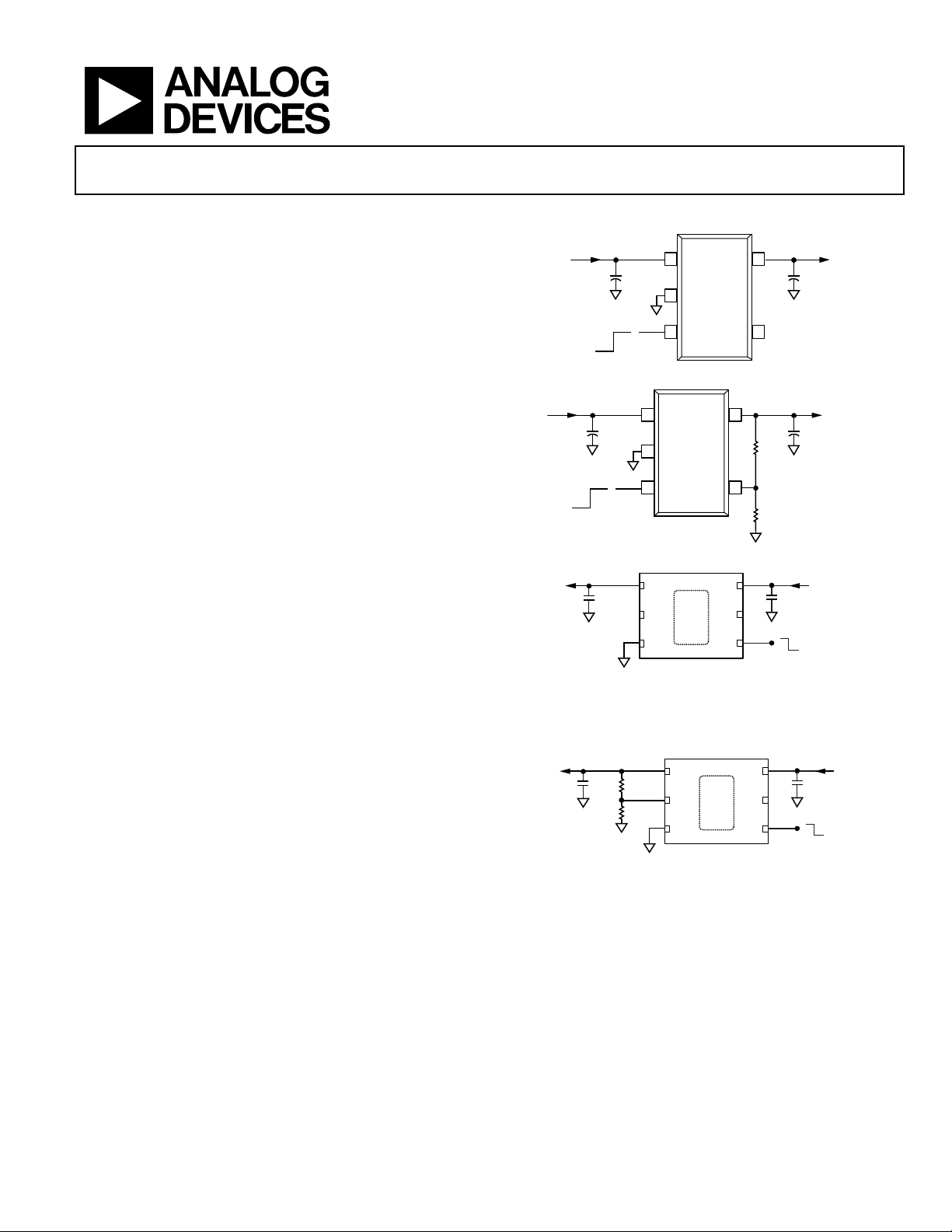
Figure 1. ADP122 with Fixed Output Voltage (TSOT Version)
Figure 2. ADP123 with Adjustable Output Voltage (TSOT Version)
GENERAL DESCRIPTION
The ADP122/ADP123 are low quiescent current, low dropout
linear regulators. They are designed to operate from an input
voltage between 2.3 V and 5.5 V and to provide up to 300 mA of
output current. The low 85 mV dropout voltage at a 300 mA load
improves efficiency and allows operation over a wide input
voltage range.
The low 170 μA of quiescent current at full load makes the ADP122
ideal for battery-operated portable equipment.
The ADP122 is capable of 31 fixed output voltages from 1.75 V
to 3.3 V. The ADP123 is the adjustable version of the device and
allows the output voltage to be set between 0.8 V and 5.0 V by
an external voltage divider.
The ADP122/ADP123 are specifically designed for stable operation
with tiny 1 µF ceramic input and output capacitors to meet the
requirements of high performance, space constrained applications.
Information furnished by Analog Devices is believed to be accurate and reliable. However, no
responsibility is assumed by Analog Devices for its use, nor for any infringements of patents or other
rights of third parties that may result from its use. Specifications subject to change without notice. No
license is granted by implication or otherwise under any patent or patent rights of Analog Devices.
Figure 3. ADP122 with Fixed Output Voltage (LFCSP Version)
Figure 4. ADP123 with Adjustable Output Voltage (LFCSP Version)
The ADP122/ADP123 have an internal soft start that gives a
constant start-up time of 350 µs. Short-circuit protection and
thermal overload protection circuits prevent damage in adverse
conditions. The ADP122/ADP123 are available in a tiny, 5-lead
TSOT package and 6-lead LFCSP package for the smallest
footprint solution to meet a variety of portable applications.
One Technology Way, P.O. Box 9106, Norwood, MA 02062-9106, U.S.A.
Tel: 781.329.4700
www.analog.com

ADP122/ADP123 Data Sheet
TABLE OF CONTENTS
Features .............................................................................................. 1
Applications ....................................................................................... 1
General Description ......................................................................... 1
Typical Application Circuits ............................................................ 1
Revision History ............................................................................... 2
Specifications ..................................................................................... 3
Recommended Specifications ..................................................... 4
Absolute Maximum Ratings ............................................................ 5
Thermal Data ................................................................................ 5
Thermal Resistance ...................................................................... 5
ESD Caution .................................................................................. 5
Pin Configurations and Function Descriptions ........................... 6
Typical Performance Characteristics ............................................. 7
REVISION HISTORY
4/12—Rev. C to Rev. D
Changes to Ordering Guide ........................................................... 21
4/12—Rev. B to Rev. C
Changes to Operating Ambient Temperature Range;
Table 3 ................................................................................................. 5
3/12—Rev. A to Rev. B
Added V
Updated Outline Dimensions ....................................................... 20
6/11—Rev. 0 to Rev. A
Added 6-Lead LFCSP Package ..................................... Throughout
Added Figure 3 and Figure 4 (Renumbered Sequentially) ......... 1
= 2.8 V to Figure 23 Caption...................................... 9
OUT
Theory of Operation ...................................................................... 11
Applications Information .............................................................. 12
Capacitor Selection .................................................................... 12
Undervoltage Lockout ............................................................... 13
Enable Feature ............................................................................ 13
Current Limit and Thermal Overload Protection ................. 14
Thermal Considerations ............................................................ 14
Junction Temperature Calculations For TSOT Package ....... 15
Junction Temperature Calculations For LFCSP Package ...... 17
Printed Circuit Board Layout Considerations........................ 19
Outline Dimensions ....................................................................... 20
Ordering Guide .......................................................................... 21
Changes to Table 4 ............................................................................. 5
Changes to Pin Configuration and Function Descriptions
Section ................................................................................................. 6
Changes to Thermal Considerations Section ............................. 14
Added Junction Temperature Calculations for LFCSP Package
Section .............................................................................................. 17
Updated Outline Dimensions ...................................................... 20
Changes to Ordering Guide .......................................................... 21
10/09—Revision 0: Initial Version
Rev. D | Page 2 of 24
Data Sheet ADP122/ADP123
SPECIFICATIONS
Unless otherwise noted, VIN = (V
C
= 1.0 µF; TA = 25°C.
OUT
Table 1.
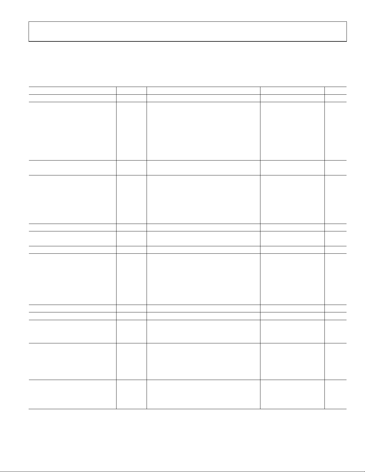
Parameter Symbol Test Conditions Min Typ Max Unit
INPUT VOLTAGE RANGE VIN 2.3 5.5 V
OPERATING SUPPLY CURRENT1 I
I
I
I
I
I
I
I
SHUTDOWN CURRENT ISD EN = GND 0.1 µA
EN = GND, TJ = −40°C to +125°C 1 µA
OUTPUT VOLTAGE ACCURACY2 V
Fixed Output I
100 µA < I
Adjustable Output I
100 µA < I
LINE REGULATION ∆V
LOAD REGULATION3 ∆V
I
ADJ INPUT BIAS CURRENT ADJ
DROPOUT VOLTAGE4 V
I
I
I
I
I
I
START-UP TIME5 t
CURRENT LIMIT THRESHOLD6 I
THERMAL SHUTDOWN
Thermal Shutdown Threshold TSSD TJ rising 150
Thermal Shutdown Hysteresis TS
EN INPUT
EN Input Logic High VIH 2.3 V ≤ VIN ≤ 5.5 V 1.2 V
EN Input Logic Low VIL 2.3 V ≤ VIN ≤ 5.5 V 0.4 V
EN Input Leakage Current V
EN = VIN or GND, TJ = −40°C to +125°C 1 µA
UNDERVOLTAGE LOCKOUT UVLO
Input Voltage Rising UVLO
Input Voltage Falling UVLO
Hysteresis UVLO
+ 0.3 V) or 2.3 V, whichever is greater; ADJ connected to VOUT; I
OUT
I
GND
OUT
/∆VIN VIN = VIN = 2.3 V to 5.5 V, TJ = −40°C to +125°C −0.05 +0.05 %/V
OUT
/∆I
OUT
OUT
2.3 V ≤ VIN ≤ 5.5 V, ADJ connected to VOUT 15 nA
I-BIAS
DROPOUT
V
STA RT-UP
350 500 650 mA
LIMIT
15
SD-HYS
EN = VIN or GND 0.1 µA
I-LEAKAGE
TJ = −40°C to +125°C 2.1 V
RISE
TJ = −40°C to +125°C 1.5 V
FAL L
TA = 25°C 125 mV
HYS
= 0 µA 45 µA
OUT
= 0 µA, TJ = −40°C to +125°C 105 µA
OUT
= 1 mA 60 µA
OUT
= 1 mA, TJ = −40°C to +125°C 120 µA
OUT
= 150 mA 130 µA
OUT
= 150 mA, TJ = −40°C to +125°C 190 µA
OUT
= 300 mA 170 µA
OUT
= 300 mA, TJ = −40°C to +125°C 240 µA
OUT
= 10 mA −1 +1 %
OUT
< 300 mA, VIN = (V
OUT
= −40°C to +125°C
= 10 mA 0.495 0.500 0.505 V
< 300 mA, VIN = 2.3 V to 5.5 V,
OUT
= −40°C to +125°C
= 1 mA to 300 mA 0.0005 %/mA
= 1 mA to 300 mA , TJ = −40°C to +125°C 0.001 %/mA
= 10 mA, V
> 2.3 V 3 mV
OUT
= 10 mA, TJ = −40°C to +125°C 5 mV
= 150 mA, V
OUT
> 2.3 V
= 150 mA, TJ = −40°C to +125°C 75 mV
= 300 mA, V
OUT
> 2.3V
= 300 mA, TJ = −40°C to +125°C 150 mV
= 3.0 V 350 µs
I
T
T
J
OUT
J
OUT
OUT
OUT
OUT
OUT
OUT
OUT
OUT
OUT
+ 0.5 V) to 5.5 V,
OUT
= 10 mA; CIN = 1.0 µF;
OUT
−2 +1.5 %
0.490 0.500 0.5075 V
45 mV
85 mV
°C
°C
Rev. D | Page 3 of 24

ADP122/ADP123 Data Sheet
10 Hz to 100 kHz, VIN = 5.5 V, V
= 4.2 V
65 µV rms
Parameter Symbol Test Conditions Min Typ Max Unit
OUTPUT NOISE OUT
10 Hz to 100 kHz, VIN = 5.5 V, V
10 Hz to 100 kHz, VIN = 5.5 V, V
10 Hz to 100 kHz, VIN = 5.5 V, V
POWER SUPPLY REJECTION RATIO PSRR 10 kHz, V
(VIN = V
+ 0.5 V) 10 kHz, V
OUT
10 kHz, V
100 kHz, V
100 kHz, V
100 kHz, V
1
The current from the external resistor divider network in the case of adjustable voltage output (as with the ADP123) should be subtracted from the ground current measured.
2
Accuracy when VOUT is connected directly to ADJ. When VOUT voltage is set by external feedback resistors, absolute accuracy in adjust mode depends on the tolerances of
the resistors used.
3
Based on an endpoint calculation using 1 mA and 300 mA loads.
4
Dropout voltage is defined as the input-to-output voltage differential when the input voltage is set to the nominal output voltage. This applies only for output voltages
greater than 2.3 V.
5
Start-up time is defined as the time between the rising edge of EN to VOUT being at 90% of its nominal value.
6
Current limit threshold is defined as the current at which the output voltage drops to 90% of the specified typical value. For example, the current limit for a 3.3 V
output voltage is defined as the current that causes the output voltage to drop to 90% of 3.3V, or 2.97 V.
10 Hz to 100 kHz, VIN = 5.5 V, V
NOISE
= 3.3 V 60 dB
OUT
= 2.5 V 60 dB
OUT
= 1.8 V 60 dB
OUT
= 3.3 V 60 dB
OUT
= 2.5 V 60 dB
OUT
= 1.8 V 60 dB
OUT
= 1.2 V 25 µV rms
OUT
= 1.8 V 35 µV rms
OUT
= 2.5 V 45 µV rms
OUT
= 3.3 V 55 µV rms
OUT
OUT
RECOMMENDED SPECIFICATIONS
Table 2.
Parameter Symbol Test Conditions Min Typ Max Unit
Minimum Input and Output
Capacitance
1
Capacitor ESR R
1
The minimum input and output capacitance should be greater than 0.70 µF over the full range of operating conditions. The full range of operating conditions in the
application must be considered during device selection to ensure that the minimum capacitance specification is met. X7R and X5R type capacitors are recommended;
Y5V and Z5U capacitors are not recommended for use with any LDO.
TA = −40°C to +125°C 0.70 µF
CAP
MIN
TA = −40°C to +125°C 0.001 1 Ω
ESR
Rev. D | Page 4 of 24
Data Sheet ADP122/ADP123
ADJ to GND
−0.3 V to +4 V
ABSOLUTE MAXIMUM RATINGS
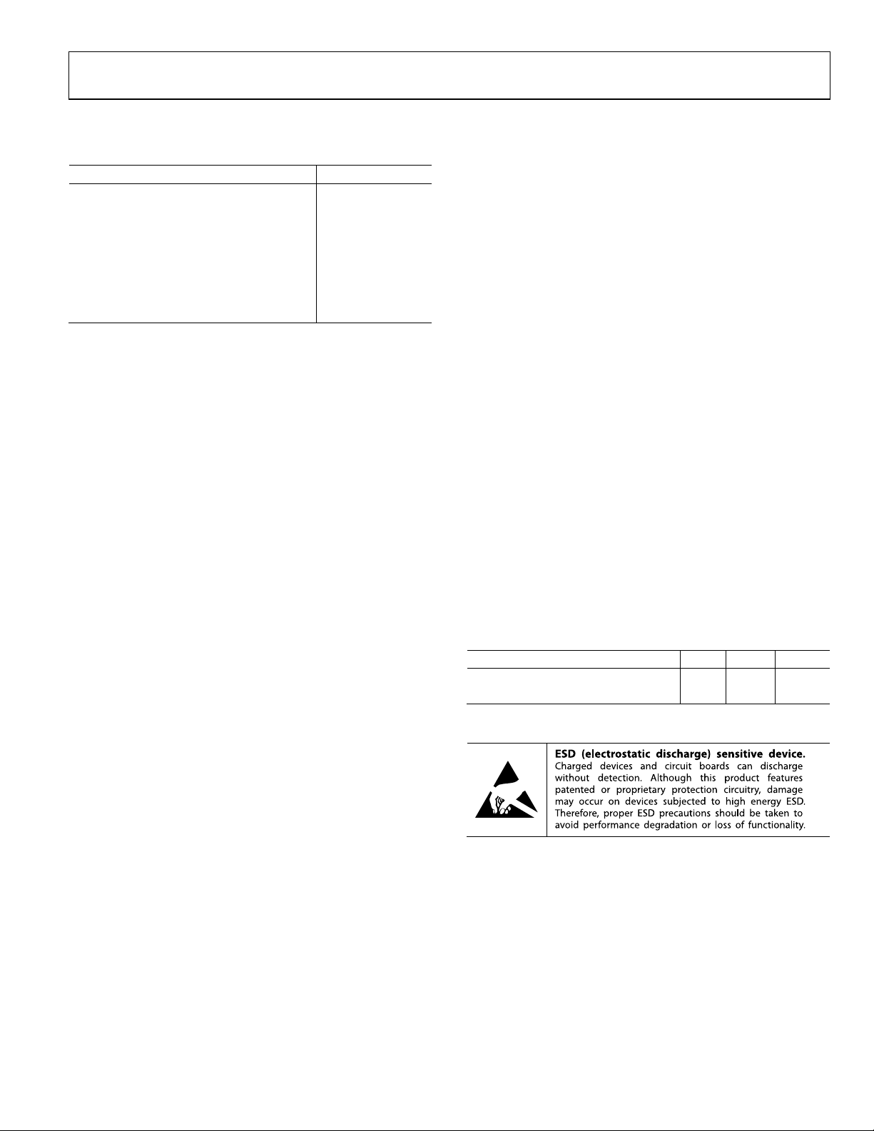
Table 3.
Parameter Rating
VIN to GND −0.3 V to +6.5 V
EN to GND −0.3 V to +6.5 V
VOUT to GND −0.3 V to VIN
Storage Temperature Range −65°C to +150°C
Operating Ambient Temperature Range −40°C to +125°C
Operating Junction Temperature −40°C to +125°C
Soldering Conditions JEDEC J-STD-020
Stresses above those listed under Absolute Maximum Ratings may
cause permanent damage to the device. This is a stress rating
only; functional operation of the device at these or any other
conditions above those indicated in the operational section of
this specification is not implied. Exposure to absolute maximum
rating conditions for extended periods may affect device reliability.
THERMAL DATA
Absolute maximum ratings apply individually only, not in
combination. The ADP122/ADP123 can be damaged when the
junction temperature limits are exceeded. Monitoring ambient
temperature does not guarantee that T
specified temperature limits. In applications with high power
dissipation and poor thermal resistance, the maximum ambient
temperature may have to be derated.
In applications with moderate power dissipation and low PCB
thermal resistance, the maximum ambient temperature can
exceed the maximum limit as long as the junction temperature
is within specification limits. The junction temperature (T
the device is dependent on the ambient temperature (T
power dissipation of the device (P
thermal resistance of the package (θ
Maximum junction temperature (T
ambient temperature (T
) and power dissipation (PD) using the
A
formula
T
= TA + (PD × θJA)
J
The junction-to-ambient thermal resistance (θ
is based on modeling and calculation using a 4-layer board. The
junction-to-ambient thermal resistance is highly dependent on the
will remain within the
J
J
), the
A
), and the junction-to-ambient
D
).
JA
) is calculated from the
J
) of the package
JA
) of
application and board layout. In applications in which high maximum power dissipation exists, close attention to thermal board
design is required. The value of θ
may vary, depending on PCB
JA
material, layout, and environmental conditions. The specified
values of θ
are based on a 4-layer, 4 inch × 3 inch circuit board.
JA
Refer to JESD51-7 for detailed information on the board
construction
Ψ
is the junction-to-board thermal characterization parameter
JB
and is measured in °C/ W. The Ψ
of the package is based on
JB
modeling and calculation using a 4-layer board. The Guidelines for
Reporting and Using Package Thermal Information: JESD51-12
states that thermal characterization parameters are not the same
as thermal resistances. Ψ
measures the component power flowing
JB
through multiple thermal paths rather than a single path as in
thermal resistance, θ
. Therefore, ΨJB thermal paths include
JB
convection from the top of the package as well as radiation from
the package—factors that make Ψ
applications. Maximum junction temperature (T
from the board temperature (T
more useful in real-world
JB
) is calculated
J
) and power dissipation (PD)
B
using the formula
T
= TB + (PD × ΨJB)
J
Refer to JESD51-8 and JESD51-12 for more detailed information
about Ψ
.
JB
THERMAL RESISTANCE
θJA and ΨJB are specified for the worst-case conditions, that is, a
device soldered in a circuit board for surface-mount packages.
Table 4. Thermal Resistance
Package Type θJA ΨJB Unit
5-Lead TSOT 170 43 °C/W
6-Lead 2 mm × 2 mm LFCSP 68.9 44.1 °C/W
ESD CAUTION
Rev. D | Page 5 of 24
ADP122/ADP123 Data Sheet
ADP122
TOP VIEW
(Not to Scale)
1
VIN
2
GND
3
EN
5
VOUT
4
NC
NC = NO CONNECT
08399-004
08399-137
TOP VIEW
(Not to Scal
e)
ADP122
3
GND
1
VOUT
2
NC
4
EN
6
VIN
5
NC
NOTES
1. NC =NOT CONNECT. THIS PIN CAN BE LEFT FLOATING
OR CONNECTED TOGROUND.
2. EXPOSED PAD MUST BE CONNECTED TO GND.
ADP123
TOP VIEW
(Not to Scale)
1
VIN
2
GND
3
EN
5
VOUT
4
ADJ
08399-003
08399-138
TOP VIEW
(Not to Scale)
ADP123
3
GND
1
VOUT
2
ADJ
4
EN
6
NOTES
1. NC =NOT CONNECT. THIS PIN CAN BE LEFTFLOATING
OR CONNECTED TOGROUND.
2. EXPOSED PAD MUST BE CONNECTED TO GND.
VIN
5
NC
PIN CONFIGURATIONS AND FUNCTION DESCRIPTIONS
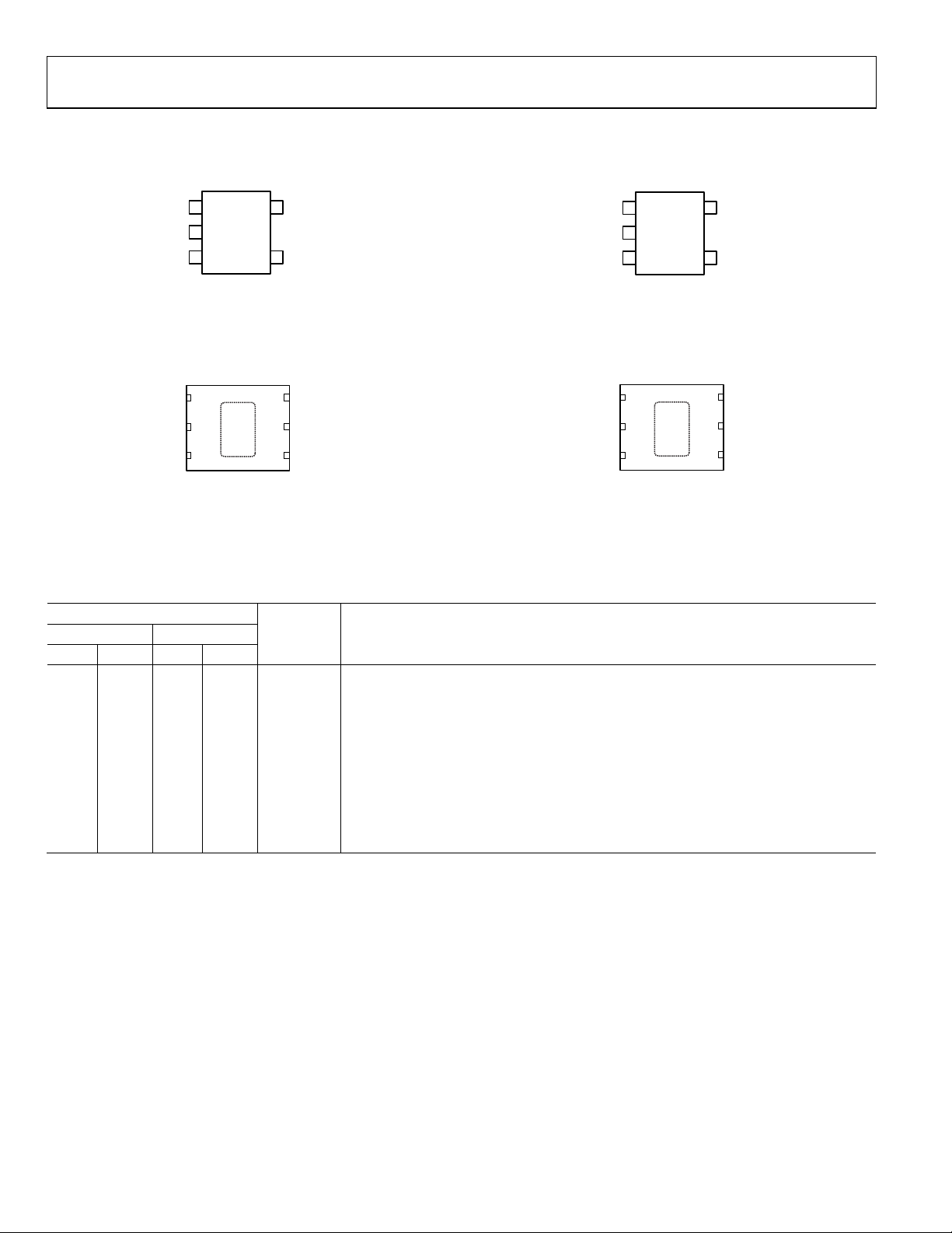
Figure 5. ADP122 TSOT Fixed Output Pin Configuration
Figure 7. ADP123 TSOT Adjustable Output Pin Configuration
Figure 6. ADP122 LFCSP Fixed Output Pin Configuration
Figure 8. ADP123 LFCSP Adjustable Output Pin Configuration
Table 5. Pin Function Descriptions
Pin No.
ADP122 ADP123
TSOT LFCSP TSOT LFCSP
Mnemonic Description
1 6 1 6 VIN Regulator Input Supply. Bypass VIN to GND with a capacitor of at least 1 µF.
2 3 2 3 GND Ground.
3 4 3 4 EN Enable Input. Drive EN high to turn on the regulator; drive EN low to turn off the
regulator. For automatic startup, connect EN to VIN.
N/A N/A 4 2 ADJ Output Voltage Adjust Input. Connect the midpoint of an external divider from VOUT to
GND to this pin to set the output voltage.
4 2, 5 N/A 5 NC No Connect. These pins are not internally bonded. They can be left floating or connected
to ground.
5 1 5 1 VOUT Regulated Output Voltage. Bypass VOUT to GND with a capacitor of at least 1 µF.
N/A EP N/A EP EPAD Exposed Pad. The exposed pad must be connected to ground.
Rev. D | Page 6 of 24
Data Sheet ADP122/ADP123
3.260
3.265
3.270
3.275
3.280
3.285
3.290
3.295
3.300
–40 –5 25 85 125
JUNCTION T E M P E RATURE (°C)
V
OUT
(V)
I
OUT
= 100µA
I
OUT
= 1mA
I
OUT
= 10mA
I
OUT
= 100mA
I
OUT
= 200mA
I
OUT
= 300mA
08399-005
3.2895
3.2900
3.2905
3.2910
3.2915
3.2920
3.2925
3.2930
3.2935
3.2940
3.2945
0.1 1 10 100 1000
I
OUT
(mA)
V
OUT
(V)
08399-006
3.284
3.286
3.288
3.290
3.292
3.294
3.296
V
IN
(V)
V
OUT
(V)
08399-007
3.6 3.8 4.0 4.2 4.4 4.6 4.8 5.0 5.2 5.4
I
OUT
= 100µA
I
OUT
= 1mA
I
OUT
= 10mA
I
OUT
= 100mA
I
OUT
= 200mA
I
OUT
= 300mA
0
50
100
150
200
250
GROUND CURRENT ( µ A)
–40 –5 25 85 125
JUNCTION T E M P E RATURE (°C)
I
OUT
= 100µA
I
OUT
= 10mA
I
OUT
= 100mA
I
OUT
= 200mA
I
OUT
= 300mA
I
OUT
= 1mA
08399-008
0
20
40
60
80
100
120
140
160
180
200
0.1 1 10 100 1000
I
OUT
(mA)
GROUND CURRENT ( µ A)
08399-009
0
20
40
60
80
100
120
140
160
180
200
3.6 3.8 4.0 4.2 4.4 4.6 4.8 5.0 5.2 5.4
V
IN
(V)
GROUND CURRENT ( µ A)
I
OUT
= 100µA
I
OUT
= 1mA
I
OUT
= 10mA
I
OUT
= 100mA
I
OUT
= 200mA
I
OUT
= 300mA
08399-010
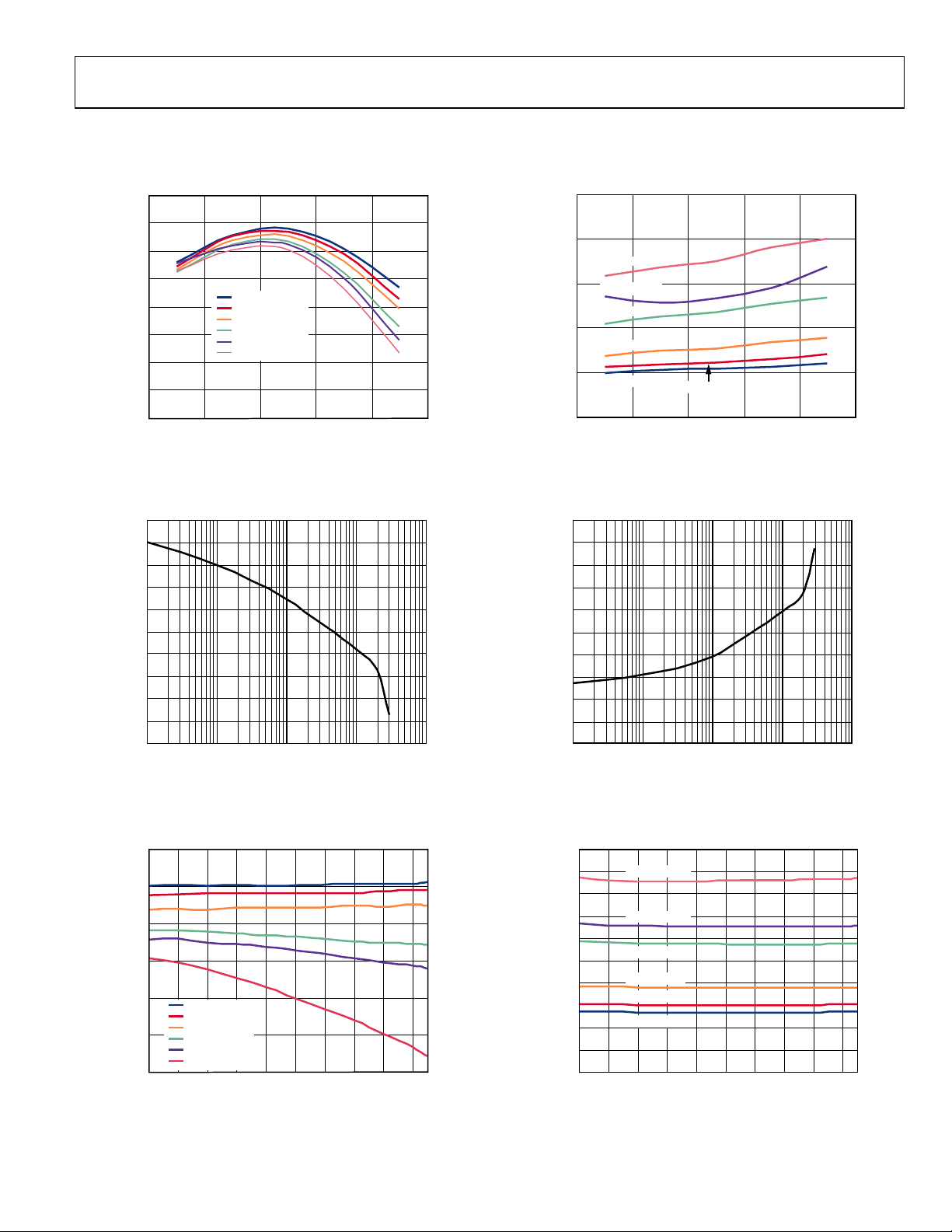
TYPICAL PERFORMANCE CHARACTERISTICS
VIN = 3.6 V, V
= 3.3 V, I
OUT
= 10 mA, CIN = 1.0 µF, C
OUT
= 1.0 µF, TA = 25°C, unless otherwise noted.
OUT
Figure 9. Output Voltage vs. Junction Temperature
Figure 10. Output Voltage vs. Load Current
Figure 12. Ground Current vs. Junction Temperature
Figure 13. Ground Current vs. Load Current
Figure 11. Output Voltage vs. Input Voltage
Figure 14. Ground Current vs. Input Voltage
Rev. D | Page 7 of 24
ADP122/ADP123 Data Sheet
0.10
0.15
0.20
0.25
0.30
0.35
0.40
0.45
0.50
–50 –25 0 25 50 75 100 125
TEMPERATURE (°C)
SHUTDOWN CURRE NT (µA)
V
IN
= 3.6V
V
IN
= 3.8V
V
IN
= 4.2V
V
IN
= 4.4V
V
IN
= 5.0V
V
IN
= 5.2V
V
IN
= 5.4V
V
IN
= 5.5V
08399-011
0
10
20
30
40
50
60
70
1 10 100 1000
I
OUT
(mA)
DROPOUT ( mV )
08399-012
0
50
100
150
200
250
300
350
400
450
3.05 3.10 3.15 3.20 3.25 3.30 3.35 3.40 3.45
VIN (V)
I
GND
(µA)
I
OUT
= 10mA
I
OUT
= 100mA
I
OUT
= 150mA
I
OUT
= 300mA
08399-014
3.00
3.05
3.10
3.15
3.20
3.25
3.30
3.35
3.05 3.10 3.15 3.20 3.25 3.30 3.35 3.40
V
IN
(V)
V
OUT
(V)
I
OUT
= 10mA
I
OUT
= 100mA
I
OUT
= 150mA
I
OUT
= 300mA
08399-013
–100
–90
–80
–70
–60
–50
–40
–30
–20
–10
10 100 1k 10k 100k 1M
10M
FREQUENCY ( Hz )
PSRR (dB)
I
OUT
= 100µA
V
IN
= V
OUT
+ 0.5V
V
RIPPLE
= 50mV
C
IN
= C
OUT
1µF
I
OUT
= 1mA
I
OUT
= 10mA
I
OUT
= 100mA
I
OUT
= 200mA
I
OUT
= 300mA
08399-015
–100
–90
–80
–70
–60
–50
–40
–30
–20
–10
10 100 1k 10k 100k 1M 10M
FREQUENCY ( Hz )
PSRR (dB)
I
OUT
= 100µA
V
IN
= V
OUT
+ 0.5V
V
RIPPLE
= 50mV
C
IN
= C
OUT
1µF
I
OUT
= 1mA
I
OUT
= 10mA
I
OUT
= 100mA
I
OUT
= 200mA
I
OUT
= 300mA
08399-016
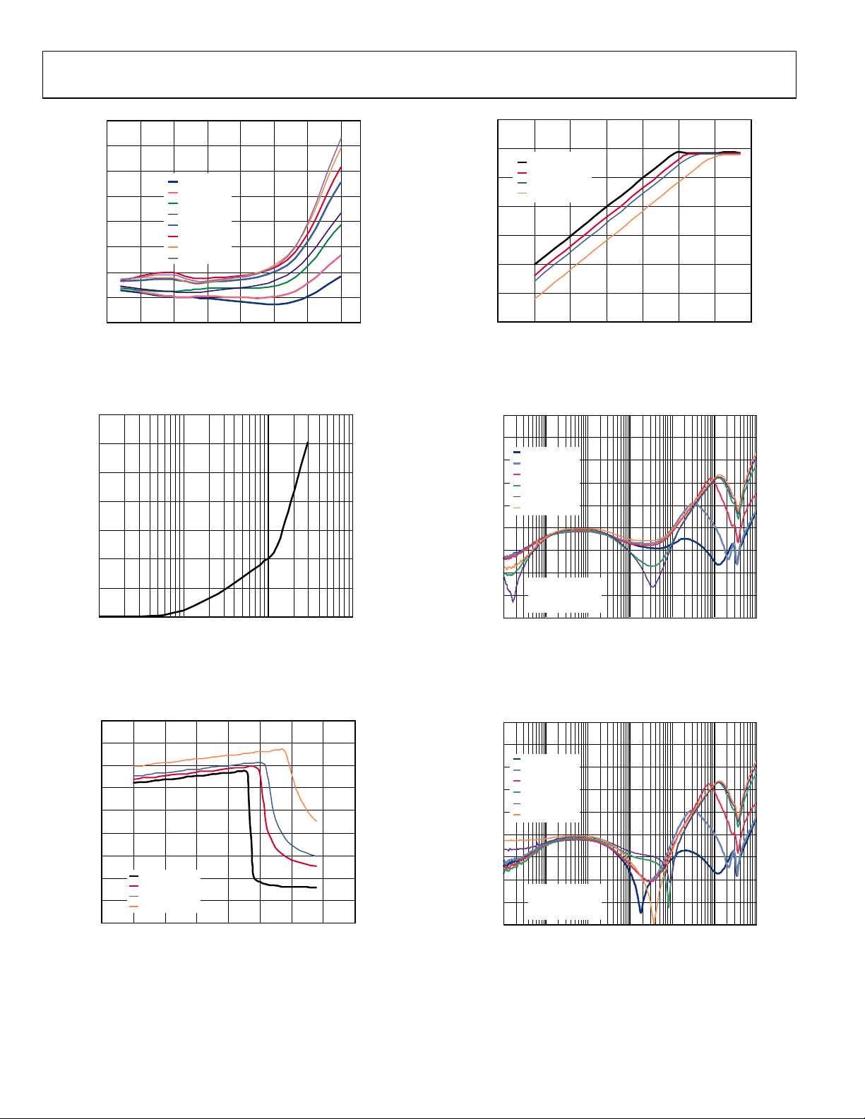
Figure 15. Shutdown Current vs. Temperature at Various Input Voltages
Figure 16. Dropout Voltage vs. Load Current
Figure 18. Output Voltage vs. Input Voltage (in Dropout)
Figure 19. Power Supply Rejection Ratio v s. Frequency, V
= 2.8 V, VIN = 3.3 V
OUT
Figure 17. Ground Current vs. Input Voltage (in Dropout)
Figure 20. Power Supply Rejection Ratio v s. Frequency, V
= 3.3 V, VIN = 3.8 V
OUT
Rev. D | Page 8 of 24
 Loading...