Analog Devices ADP1173 Datasheet

Micropower
SET
V
IN
GAIN BLOCK/
ERROR AMP
COMPARATOR
SW2
FBGND
SW1
AO
I
LIM
OSCILLATOR
DRIVER
A1
A2
1.245V
REFERENCE
ADP1173
SET
V
IN
GAIN BLOCK/
ERROR AMP
COMPARATOR
SW2
SENSEGND
SW1
AO
I
LIM
OSCILLATOR
DRIVER
A1
A2
1.245V
REFERENCE
ADP1173-3.3
ADP1173-5
ADP1173-12
R2
753kΩ
R1
ADP1173-3.3: R1 = 456kΩ
ADP1173-5: R1 = 250kΩ
ADP1173-12: R1 = 87.4kΩ
a
FEATURES
Operates From 2.0 V to 30 V Input Voltages
Only 110 mA Supply Current (Typical)
Step-Up or Step-Down Mode Operation
Very Few External Components Required
Low Battery Detector On-Chip
User-Adjustable Current Limit
Internal 1 A Power Switch
Fixed or Adjustable Output Voltage Versions
8-Pin DIP or SO-8 Package
APPLICATIONS
Notebook and Palmtop Computers
Cellular Telephones
Flash Memory V
3 V to 5 V, 5 V to 12 V Converters
9 V to 5 V, 12 V to 5 V Converters
Portable Instruments
LCD Bias Generators
GENERAL DESCRIPTION
The ADP1173 is part of a family of step-up/step-down switching
regulators that operates from an input supply voltage of as little as
2 V to 12 V in step-up mode and to 30 V in step-down mode.
The ADP1173 consumes as little as 110 µA in standby mode,
making it ideal for applications that need low quiescent current.
An auxiliary gain amplifier can serve as a low battery detector,
linear regulator (under voltage lockout) or error amplifier.
The ADP1173 can deliver 80 mA at 5 V from a 3 V input in
step-up configuration or 100 mA at 5 V from a 12 V input in
step-down configuration. For input voltages of less than 2 V use
the ADP1073.
Generators
pp
DC-DC Converter
ADP1173
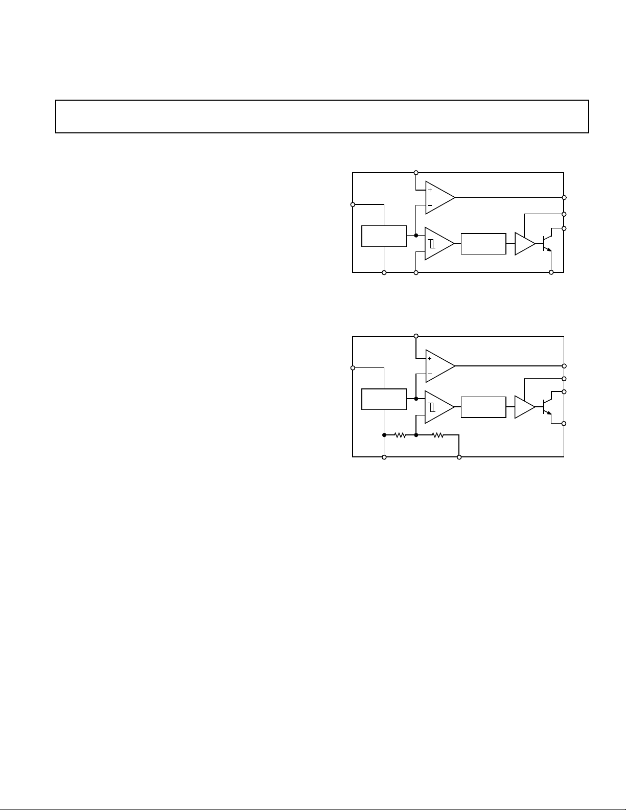
FUNCTIONAL BLOCK DIAGRAMS
REV. 0
Information furnished by Analog Devices is believed to be accurate and
reliable. However, no responsibility is assumed by Analog Devices for its
use, nor for any infringements of patents or other rights of third parties
which may result from its use. No license is granted by implication or
otherwise under any patent or patent rights of Analog Devices.
One Technology Way, P.O. Box 9106, Norwood, MA 02062-9106, U.S.A.
Tel: 617/329-4700 World Wide Web Site: http://www.analog.com
Fax: 617/326-8703 © Analog Devices, Inc., 1997

ADP1173–SPECIFICATIONS
(@ TA = 08C to +708C, VIN = 3 V unless otherwise noted)
Model Symbol Conditions Min Typ Max Units
QUIESCENT CURRENT I
QUIESCENT CURRENT, BOOST MODE I
Q
Q
Switch Off 110 150 µA
No Load, T
= +25°C
A
CONFIGURATION ADP1173-3.3 135 µA
ADP1173-5 135 µA
ADP1173-12 250 µA
INPUT VOLTAGE V
IN
Step-Up Mode 2.0 12.6 V
Step-Down Mode 30 V
COMPARATOR TRIP POINT VOLTAGE ADP1173
OUTPUT SENSE VOLTAGE V
OUT
ADP1173-3.3
ADP1173-5
ADP1173-12
1
2
2
2
1.20 1.245 1.30 V
3.14 3.30 3.46 V
4.75 5.00 5.25 V
11.4 12.0 12.6 V
COMPARATOR HYSTERESIS ADP1173 5 12 mV
OUTPUT HYSTERESIS ADP1173-3.3 13 35 mV
ADP1173-5 20 55 mV
ADP1173-12 50 100 mV
OSCILLATOR FREQUENCY f
OSC
16 24 32 kHz
DUTY CYCLE Full Load 43 55 63 %
SWITCH ON TIME t
ON
FEEDBACK PIN BIAS CURRENT ADP1173, V
SET PIN BIAS CURRENT V
GAIN BLOCK OUTPUT LOW V
OL
REFERENCE LINE REGULATION 2.0 V ≤ V
SW
VOLTAGE, STEP-UP MODE V
SAT
SW
VOLTAGE, STEP-DOWN MODE V
SAT
GAIN BLOCK GAIN A
SAT
SAT
V
CURRENT LIMIT 220 Ω from I
I
Tied to V
LIM
= V
SET
I
= 100 µA, V
SINK
5 V ≤ V
V
= 3.0 V, ISW = 650 mA 0.5 0.85 V
IN
V
= 5.0 V, I
IN
T
= +25°C 0.8 1.0 V
A
V
= 5.0 V, ISW = 1 A 1.4 V
IN
V
= 12 V, T
IN
I
= 650 mA 1.1 1.5 V
SW
V
= 12 V, ISW = 650 mA 1.7 V
IN
R
= 100 kΩ
L
T
= +25°C
A
IN
= 0 V 60 290 nA
FB
REF
= 1.00 V 0.15 0.4 V
SET
≤ 5 V 0.2 0.4 %/V
IN
≤ 30 V 0.02 0.075 %/V
IN
= 1 A,
SW
= +25°C,
A
3
to V
LIM
IN
15 23 32 µs
70 150 nA
400 1000 V/V
400 mA
CURRENT LIMIT TEMPERATURE
COEFFICIENT –0.3 %/°C
SWITCH-OFF LEAKAGE CURRENT Measured at SW1 Pin 1 10 µA
T
= +25°C
A
MAXIMUM EXCURSION BELOW GND V
NOTES
1
This specification guarantees that both the high and low trip points of the comparator fall within the 1.20 V to 1.30 V range.
2
The output voltage waveform will exhibit a sawtooth shape due to the comparator hysteresis. The output voltage on the fixed output versions will always be within
the specified range.
3
100 kΩ resistor connected between a 5 V source and the AO pin.
Specifications subject to change without notice.
SW2
I
≤ 10 µA, Switch Off –400 –350 mV
SW1
T
= +25°C
A
–2–
REV. 0

ADP1173
WARNING!
ESD SENSITIVE DEVICE
AO
I
LIM
SW1
GND
V
IN
SW2
*FIXED VERSIONS
1
2
3
4
8
7
6
5
ADP1173
TOP VIEW
(Not to Scale)
FB (SENSE)*
SET
AO
I
LIM
SW1
GND
V
IN
SW2
*FIXED VERSIONS
1
2
3
4
8
7
6
5
ADP1173
TOP VIEW
(Not to Scale)
FB (SENSE)*
SET
ABSOLUTE MAXIMUM RATINGS*
Supply Voltage (VIN) . . . . . . . . . . . . . . . . . . . . . . . . . . . . 36 V
SW1 Pin Voltage (V
SW2 Pin Voltage (V
) . . . . . . . . . . . . . . . . . . . . . . . . . 50 V
SW1
) . . . . . . . . . . . . . . . . . . –0.5 V to V
SW2
IN
Feedback Pin Voltage (ADP1173) . . . . . . . . . . . . . . . . . . . 5 V
Sense Pin Voltage (ADP1173, –3.3, –5, –12) . . . . . . . . . 36 V
Maximum Power Dissipation . . . . . . . . . . . . . . . . . . 500 mW
Maximum Switch Current . . . . . . . . . . . . . . . . . . . . . . . .1.5 A
Operating Temperature Range . . . . . . . . . . . . . 0°C to +70°C
Storage Temperature Range . . . . . . . . . . . . . –65°C to 150°C
Lead Temperature, (Soldering, 10 sec) . . . . . . . . . . . .+300°C
*Stresses above those listed under Absolute Maximum Ratings may cause perma-
nent damage to the device. This is a stress rating only; functional operation of the
device at these or any other conditions above those listed in the operational
sections of this specification is not implied. Exposure to absolute maximum
ratings for extended periods of time may affect device reliability.
ORDERING GUIDE
Output Package
Model Voltage Options*
ADP1173AN ADJ N-8
ADP1173AR ADJ SO-8
ADP1173AN-3.3 3.3 V N-8
ADP1173AR-3.3 3.3 V SO-8
ADP1173AN-5 5 V N-8
ADP1173AR-5 5 V SO-8
ADP1173AN-12 12 V N-8
ADP1173AR-12 12 V SO-8
*N = Plastic DIP, SO = Small Outline Package.
L1*
+
4X NICAD
OR
ALKALINE
CELLS
*L1 = COILTRONICS CTX100-4
470µF
7
56Ω
1
I
LIMVIN
ADP1173
SET
5
100µH
2
3
SW1
6
AO
FB
8
SW2GND
4
+
470µF
IRF7203
470kΩ
240Ω
24kΩ
75kΩ
+5V
OUTPUT
AT 100mA
+
470µF
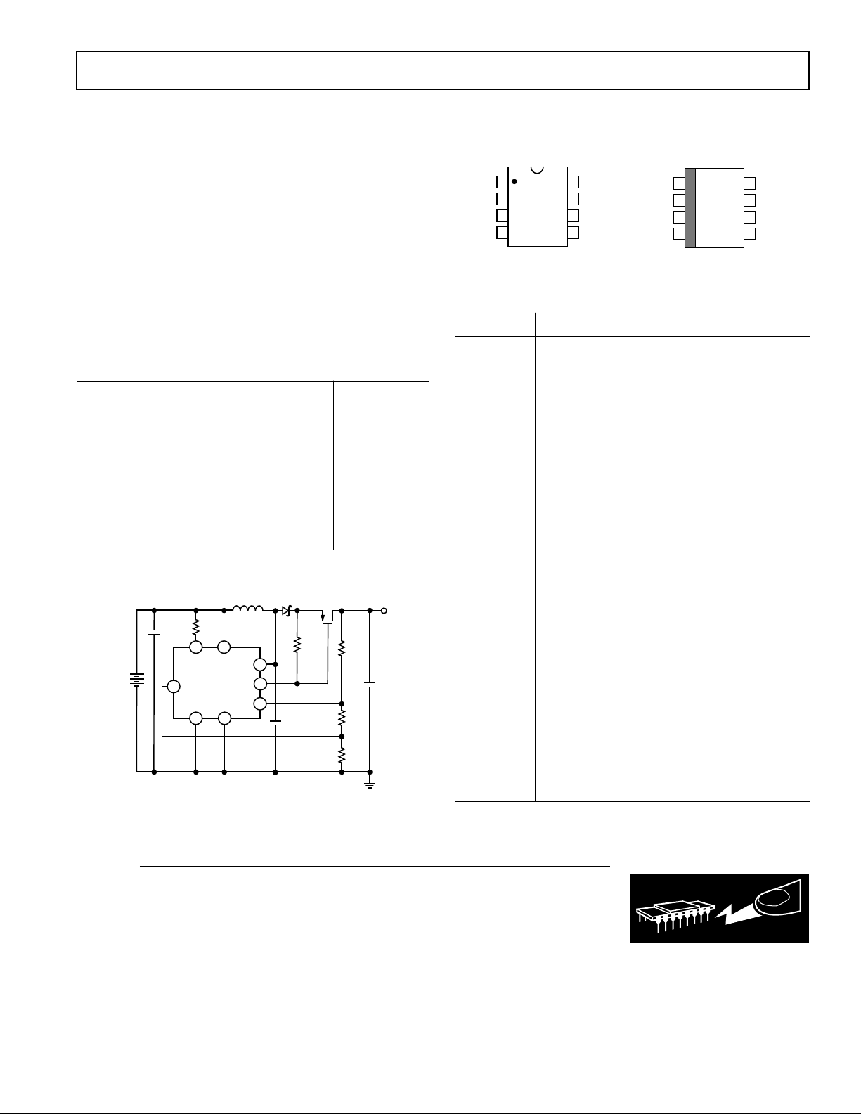
PIN CONFIGURATIONS
N-8 SO-8
8-Lead Plastic DIP 8-Lead Plastic SO
PIN FUNCTION DESCRIPTIONS
Mnemonic Function
I
LIM
For normal conditions this pin is connected to
V
. When lower current is required, a resistor
IN
should be connected between I
LIM
and V
IN.
Limiting the switch current to 400 mA is
achieved by connecting a 220 Ω resistor.
V
IN
Input Voltage.
SW1 Collector Node of Power Transistor.
For step-down configuration, connect to V
;
IN
for step-up configuration, connect to an
inductor/diode.
SW2 Emitter Node of Power Transistor. For step-
down configuration, connect to inductor/
diode; for step-up configuration, connect to
ground. Do not allow this pin to drop more
than a diode drop below ground.
GND Ground.
AO Auxiliary Gain (GB) Output. The open
collector can sink 100 µA.
SET Gain Amplifier Input. The amplifier has
positive input connected to the SET pin and
negative input is connected to 1.245 V
reference.
FB/SENSE On the ADP1173 (adjustable) version this pin
is connected to the comparator input. On the
ADP1173-3.3, ADP1173-5 and ADP1173-12,
the pin goes directly to the internal application
resistor that sets the output voltage.
Figure 1. Step-Up or Step-Down Converter
CAUTION
ESD (electrostatic discharge) sensitive device. Electrostatic charges as high as 4000 V readily
accumulate on the human body and test equipment and can discharge without detection.
Although the ADP1173 features proprietary ESD protection circuitry, permanent damage may
occur on devices subjected to high energy electrostatic discharges. Therefore, proper ESD
precautions are recommended to avoid performance degradation or loss of functionality.
REV. 0
–3–

ADP1173
TEMPERATURE – °C
120
110
40
–40 0 8525 70
80
70
60
50
100
90
QUIESCENT CURRENT – µA
QUIESCENT CURRENT
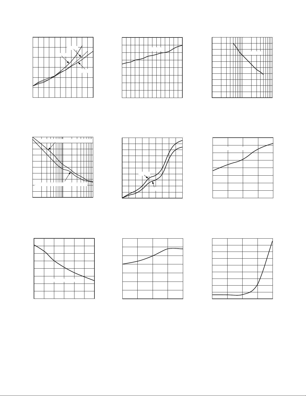
–Typical Performance Characteristics
1.2
1.0
0.8
0.6
(SAT) – V
CE
V
0.4
0.2
0
0.2 1.20.4 0.6 0.8 1.0
SWITCH CURRENT – A
VIN = 3V
VIN = 2V
VIN = 5V
Figure 2. Saturation Voltage vs.
Switch Current in Step-Up Mode
1000
VIN =24V WITH L = 500µH @ V
900
800
700
600
500
400
300
SWITCH CURRENT – mA
VIN =12V WITH L = 250µH @ V
200
100
0
100 1000
R
– Ω
LIM
OUT
OUT
= 5V
= 5V
1.6
1.4
1.2
1.0
0.8
0.6
0.4
SWITCH ON VOLTAGE – V
0.2
0.0
0.15 0.25 0.35 0.45 0.55 0.65
0.05
V
CE(SAT)
SWITCH CURRENT – A
0.75
Figure 3. Switch ON Voltage vs.
Switch Current in Step-Down Mode
100
90
80
70
60
50
40
30
SUPPLY CURRENT – mA
20
10
0
0 100 900
VIN = 5V
VIN = 2V
200 300 400 600 700 800500
SWITCH CURRENT – mA
1100
1000
900
800
700
600
500
400
SWITCH CURRENT – mA
300
200
100
10 100 1000
2V < VIN < 5V
R
– Ω
LIM
Figure 4. Maximum Switch Current
vs. R
in Step-Up Mode
LIM
Figure 5. Maximum Switch Current
vs. R
in Step-Down Mode
LIM
25.5
25
24.5
24
23.5
23
22.5
OSCILLATOR FREQUENCY – kHz
22
21.5
OSCILLATOR FREQUENCY
35 30
10 15
INPUT VOLTAGE – Volts
Figure 8. Oscillator Frequency vs.
Input Voltage
20 25
Figure 6. Supply Current vs.
Switch Current
80
70
60
50
40
30
SET PIN BIAS CURRENT – nA
20
10
–40 0 85
TEMPERATURE – °C
V
= 3V
IN
25 70
Figure 9. Set Pin Bias Current vs.
Temperature
–4–
Figure 7. Quiescent Current vs.
Temperature
450
400
350
300
250
200
150
100
50
FEEDBACK PIN BIAS CURRENT – nA
0
–40 0 85
TEMPERATURE – °C
= 3V
V
IN
25 70
Figure 10. Feedback Pin Bias Current
vs. Temperature
REV. 0

ADP1173
APPLICATIONS
Theory of Operation
The ADP1173 is a flexible, low power switch mode power
supply (SMPS) controller. The regulated output voltage can be
greater than the input voltage (boost or step-up mode) or less
than the input (buck or step-down mode). This device uses a
gated-oscillator technique to provide very high performance
with low quiescent current.
A functional block diagram of the ADP1173 is shown on the
front page. The internal 1.245 V reference is connected to one
input of the comparator, while the other input is externally
connected (via the FB pin) to a feedback network connected to
the regulated output. When the voltage at the FB pin falls below
1.245 V, the 24 kHz oscillator turns on. A driver amplifier provides base drive to the internal power switch, and the switching
action raises the output voltage. When the voltage at the FB pin
exceeds 1.245 V, the oscillator is shut off. While the oscillator is
off, the ADP1173 quiescent current is only 110 µA. The com-
parator includes a small amount of hysteresis, which ensures
loop stability without requiring external components for frequency compensation.
The maximum current in the internal power switch can be set
by connecting a resistor between V
and the I
IN
pin. When the
LIM
maximum current is exceeded, the switch is turned OFF. The
current limit circuitry has a time delay of about 2 µs. If an
external resistor is not used, connect I
information on I
is included in the Limiting the Switch
LIM
to VIN. Further
LIM
Current section of this data sheet.
The ADP1173 internal oscillator provides 23 µs ON and 19 µs
OFF times, which is ideal for applications where the ratio
between V
and V
IN
is roughly a factor of two (such as
OUT
converting +3 V to + 5 V). However, wider range conversions
(such as generating +12 V from a +5 V supply) can easily be
accomplished.
An uncommitted gain block on the ADP1173 can be connected
as a low battery detector. The inverting input of the gain block
is internally connected to the 1.245 V reference. The noninverting input is available at the SET pin. A resistor divider, connected between V
and GND with the junction connected to
IN
the SET pin, causes the AO output to go LOW when the low
battery set point is exceeded. The AO output is an open
collector NPN transistor which can sink 100 µA.
The ADP1173 provides external connections for both the
collector and emitter of its internal power switch, which permits
both step-up and step-down modes of operation. For the stepup mode, the emitter (pin SW2) is connected to GND and the
collector (pin SW1) drives the inductor. For step-down mode,
the emitter drives the inductor while the collector is connected
to V
.
IN
The output voltage of the ADP1173 is set with two external
resistors. Three fixed-voltage models are also available:
ADP1173-3.3 (+3.3 V), ADP1173-5 (+5 V) and ADP1173-12
(+12 V). The fixed-voltage models are identical to the ADP1173,
except that laser-trimmed voltage-setting resistors are included
on the chip. On the fixed-voltage models of the ADP1173,
simply connect the feedback pin (Pin 8) directly to the output
voltage.
COMPONENT SELECTION
General Notes on Inductor Selection
When the ADP1173 internal power switch turns on, current
begins to flow in the inductor. Energy is stored in the inductor
core while the switch is on, and this stored energy is then
transferred to the load when the switch turns off. Both the
collector and the emitter of the switch transistor are accessible
on the ADP1173, so the output voltage can be higher, lower or
of opposite polarity than the input voltage.
To specify an inductor for the ADP1173, the proper values of
inductance, saturation current and dc resistance must be
determined. This process is not difficult, and specific equations
for each circuit configuration are provided in this data sheet. In
general terms, however, the inductance value must be low
enough to store the required amount of energy (when both
input voltage and switch ON time are at a minimum) but high
enough that the inductor will not saturate when both V
IN
and
switch ON time are at their maximum values. The inductor
must also store enough energy to supply the load without
saturating. Finally, the dc resistance of the inductor should be
low, so that excessive power will not be wasted by heating the
windings. For most ADP1173 applications, an inductor of
47 µH to 470 µH, with a saturation current rating of 300 mA to
1 A and dc resistance <1 Ω is suitable. Ferrite core inductors
which meet these specifications are available in small, surfacemount packages.
To minimize Electro-Magnetic Interference (EMI), a toroid or
pot core type inductor is recommended. Rod core inductors are
a lower cost alternative if EMI is not a problem.
CALCULATING THE INDUCTOR VALUE
Selecting the proper inductor value is a simple three-step
process:
1. Define the operating parameters: minimum input voltage,
maximum input voltage, output voltage and output current.
2. Select the appropriate conversion topology (step-up, step-
down, or inverting).
3. Calculate the inductor value, using the equations in the
following sections.
Inductor Selection—Step-Up Converter
In a step-up, or boost, converter (Figure 14), the inductor must
store enough power to make up the difference between the
input voltage and the output voltage. The power that must be
stored is calculated from the equation:
P
where V
= V
()
L
OUT+VD–VIN(MIN )
is the diode forward voltage (≈ 0.5 V for a 1N5818
D
×I
()
OUT
(1)
Schottky). Energy is only stored in the inductor while the
ADP1173 switch is ON, so the energy stored in the inductor on
each switching cycle must be must be equal to or greater than:
P
L
f
OSC
(2)
in order for the ADP1173 to regulate the output voltage.
REV. 0
–5–
 Loading...