Analog Devices ADP1148AR, ADP1148AN-5, ADP1148AN-3.3, ADP1148AN, ADP1148AR-5 Datasheet
...
High Efficiency Synchronous
Q
R
S
V
TH1
V
IN
SENSE(–)
V
TH2
1.25V
OFF-TIME
CONTROL
100kV
13kV
B
V
IN
P-DRIVE SENSE(+) SENSE(–)
G
4 6
C
T
I
TH
SHUTDOWN
8
13
ADP1148
10mV to
150mV
C
V
FB
INT V
CC
REFERENCE
510
T
N-DRIVE
PWR
GND
14
12
ADJUSTABLE
VERSION
V
FB
9
7
S
1
Q
R
S
2
V
SLEEP
SIGNAL
GND
11
NON-OVERLAP
DRIVE
a
ADP1148, ADP1148-3.3, ADP1148-5
FEATURES
Operation From 3.5 V to 18 V Input Voltage
Ultrahigh Efficiency > 95%
Low Shutdown Current
Current Mode Operation for Excellent Line and Load
Transient Response
High Efficiency Maintained Over Wide Current Range
Logic Controlled Micropower Shutdown
Short Circuit Protection
Very Low Dropout Operation
Synchronous FET Switching for High Efficiency
Adaptive Nonoverlap Gate Drives
APPLICATIONS
Notebook and Palmtop Computers
Portable Instruments
Battery Operated Digital Devices
Industrial Power Distribution
Avionics Systems
Telecom Power Supplies
GPS Systems
Cellular Telephones
GENERAL DESCRIPTION
The ADP1148 is part of a family of synchronous step-down
switching regulator controllers featuring automatic sleep mode
to maintain high efficiencies at low output currents. These
devices drive external complementary power MOSFETs at
switching frequencies up to 250 kHz using a constant off-time
current-mode architecture.
Step-Down Switching Regulators
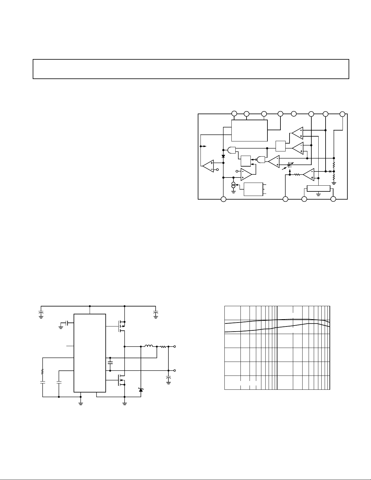
FUNCTIONAL BLOCK DIAGRAM
The constant off-time architecture maintains constant ripple
current in the inductor, easing the design of wide input range
converters. Current-mode operation provides excellent line and
load transient response. The operating current level is user
programmable via an external current sense resistor.
The ADP1148 incorporates automatic Power Saving Sleep
Mode operation when load currents drop below the level required for continuous operation. In sleep mode, standby power
is reduced to only about 2 mW at V
both MOSFETs are turned off.
= 10 V. In shutdown,
IN
TYPICAL APPLICATIONS
VIN (5.2V TO 18V)
++
C
100mF
62mH
C1
10BQ040
IN
R
L*
SENSE
0.05V
1mF
>1.5V = SHUTDOWN
R
1kV
C
3300pF
10nF
0V = NORMAL
C
C
T
470pF
C
Figure 1. High Efficiency Step-Down Converter Figure 2. ADP1148-5 Typical Efficiency
REV. A
Information furnished by Analog Devices is believed to be accurate and
reliable. However, no responsibility is assumed by Analog Devices for its
use, nor for any infringements of patents or other rights of third parties
which may result from its use. No license is granted by implication or
otherwise under any patent or patent rights of Analog Devices.
INT V
ADP1148
SHUTDOWN
I
TH
C
T
S-GND
V
IN
CC
P-DRIVE
SENSE(+)
SENSE(–)
N-DRIVE
P-GND
P-CH
IRF7204
1000pF
N-CH
IRF7403
*COILTRONICS CTX-68-4
**KRL SL-1-C1-0R050L
**
V
OUT
5V/2A
+C
390mF
OUT
100
95
90
85
EFFICIENCY – %
80
75
FIGURE 1 CIRCUIT
70
0.02 2
LOAD CURRENT – A
VIN = 6V
VIN = 10V
0.2
One Technology Way, P.O. Box 9106, Norwood, MA 02062-9106, U.S.A.
Tel: 781/329-4700 World Wide Web Site: http://www.analog.com
Fax: 781/326-8703 © Analog Devices, Inc., 1997

ADP1148, ADP1148-3.3, ADP1148-5–SPECIFICATIONS
ELECTRICAL CHARACTERISTICS
(08C ≤ TA ≤ +708C,1 VIN = 10 V, V
Parameter Symbol Conditions
2
= 0 V, unless otherwise noted. See Figure 17.)
SHUTDOWN
Min Typ Max Units
FEEDBACK VOLTAGE
ADP1148 Only V
10
VIN = 9 V 1.21 1.25 1.29 V
FEEDBACK CURRENT
ADP1148 Only I
REGULATED OUTPUT VOLTAGE V
10
OUT
ADP1148-3.3 I
ADP1148-5 I
OUTPUT VOLTAGE LINE T
REGULATION dV
OUT
VIN = 9 V
= 700 mA 3.23 3.33 3.43 V
LOAD
= 700 mA 4.9 5.05 5.2 V
LOAD
= +25°C, VIN = 7 V to 12 V,
A
I
= 50 mA –40 +40 mV
LOAD
0.2 1.0 µA
OUTPUT VOLTAGE LOAD
REGULATION dV
ADP1148-3.3 5 mA < I
ADP1148-5 5 mA < I
SLEEP MODE OUTPUT RIPPLE dV
INPUT DC SUPPLY CURRENT
3
Normal Mode V
Sleep Mode (ADP1148-3.3) V
Sleep Mode (ADP1148-5) V
Shutdown V
OUT
I
OUT
I
Q
= 0 A 50 mV p-p
LOAD
TA = +25°C
= 4 V < VIN < 18 V 1.6 2.3 mA
IN
= 4 V < VIN < 18 V 160 250 µA
IN
= 4 V < VIN < 18 V 160 250 µA
IN
SHUTDOWN
< 2 A 40 65 mV
LOAD
< 2 A 60 100 mV
LOAD
= 2.1 V, 10 20 µA
4 V < VIN < 15 V
CURRENT SENSE THRESHOLD V
VOLTAGE
4
8–V7
ADP1148 Only V
ADP1148-3.3 V
ADP1148-5 V
V9 = V
V7 = 5 V, TA = +25°C25mV
= V
9
= 5 V 130 150 170 mV
V
7
= V
7
= V
V
7
= V
7
V7 = V
/4 + 25 mV (Forced),
OUT
/4 mV – 25 mV (Forced),
OUT
+ 100 mV (Forced) 25 mV
OUT
100 mV (Forced) 130 150 170 mV
OUT –
+ 100 mV (Forced 25 mV
OUT
– 100 mV (Forced) 130 150 170 mV
OUT
SHUTDOWN PIN THRESHOLD
ADP1148-3.3, ADP1148-5 V
SHUTDOWN PIN INPUT CURRENT I
PIN DISCHARGE CURRENT I
C
T
OFF-TIME t
DRIVER OUTPUT TRANSITION t
10
10
4
OFF
, t
R
F
TA = +25°C 0.6 0.8 2.0 V
0 V < V
SHUTDOWN
TA = +25°C, V
= V
V
7
V
OUT
, 506590 µA
OUT
= 0 V 2 10 µA
CT = 390 pF, I
< 8 V, VIN = 18 V 1.2 5 µA
in Regulation,
OUT
= 700 mA 4 5 6 µs
LOAD
CL = 3000 pF (Pins 1, 14)
TIMES VIN = 6 V, TA = +25°C 100 200 ns
NOTES
1
All limits at temperature extremes are guaranteed via correlation using standard Quality Control methods. Specifications subject to change without notice.
2
TJ is calculated from the ambient temperature TA and power dissipation PD according to the following formulas:
ADP1148AR, ADP1148AR-3.3, ADP1148AR-5: TJ = TA + (PD × 110°C/W)
ADP1148AN, ADP1148AN-3.3, ADP1148AN-5: TJ = TA + (PD × 70°C/W)
3
Dynamic supply current is higher due to the gate charge being delivered at the switching frequency. The allowable operating frequency may be limited by power
dissipation at high input voltages.
4
The ADP1148 version is tested with external feedback resistors, setting the nominal output voltage to 3.3 V.
Specifications subject to change without notice.
–2–
REV. A

ADP1148, ADP1148-3.3, ADP1148-5
ELECTRICAL CHARACTERISTICS
Parameter Symbol Conditions
(–408C ≤ TA ≤ +858C,1 VIN = 10 V, V
2
= 0 V, unless otherwise noted. See Figure 17.)
SHUTDOWN
Min Typ Max Units
FEEDBACK VOLTAGE
ADP1148 Only V
REGULATED OUTPUT VOLTAGE V
10
OUT
ADP1148-3.3 I
ADP1148-5 I
INPUT DC SUPPLY CURRENT
3
I
Q
VIN = 9 V 1.20 1.25 1.30 V
VIN = 9 V
= 700 mA 3.17 3.33 3.4 V
LOAD
= 700 mA 4.85 5.05 5.2 V
LOAD
Normal Mode VIN = 4 V < VIN < 18 V 1.6 2.6 mA
Sleep Mode (ADP1148-3) V
Sleep Mode (ADP1148-5) V
Shutdown V
= 4 V < VIN < 18 V 160 280 µA
IN
= 6 V < VIN < 18 V 160 280 µA
IN
SHUTDOWN
= 2.1 V, 10 24 µA
4 V < VIN < 12 V
CURRENT SENSE THRESHOLD
VOLTAGE
ADP1148 Only V9 = V
ADP1148-3.3 V
ADP1148-5.0 V
SHUTDOWN PIN THRESHOLD V
4
V8–V
10
7
= 5 V
V
7
= V
V
9
= 5 V
V
7
= V
7
= V
V
7
= V
7
V7 = V
/4 + 25 mV (Forced), 0 mV
OUT
/4 – 25 mV (Forced), 115 150 175 mV
OUT
+ 100 mV (Forced) 0 mV
OUT
– 100 mV (Forced) 115 150 175 mV
OUT
+ 100 mV (Forced) 0 mV
OUT
– 100 mV (Forced) 115 150 175 mV
OUT
ADP1148-3.3, ADP1148-5 0.55 0.8 2 V
OFF-TIME t
NOTES
1
All limits at temperature extremes are guaranteed via correlation using standard Quality Control method.
2
TJ is calculated from the ambient temperature TA and power dissipation PD according to the following formulas:
ADP1148AR, ADP1148AR-3, ADP1148AR-5: TJ = TA + (PD × 110°C/W)
ADP1148AN, ADP1148AN-3, ADP1148AN-5: TJ = TA + (PD × 70°C/W)
3
Dynamic supply current is higher due to the gate charge being delivered at the switching frequency. The allowable operating frequency may be limited by power
dissipation at high input voltages.
4
The ADP1148 version is tested with external feedback resistors setting the nominal output voltage to 3.3 V.
Specifications subject to change without notice.
OFF
CT = 390 pF, I
= 700 mA 4 5 6.2 µs
LOAD
ABSOLUTE MAXIMUM RATINGS
Input Supply Voltage (Pin 3) . . . . . . . . . . . . . –0.3 V to +20 V
Continuous Output Currents (Pins 1, 14) . . . . . . . . . . 50 mA
Sense Voltages (Pins 7, 8) . . . . . . . . . . . . . . . . –0.3 V to V
CC
Operating Temperature Range . . . . . . . . . . . . 0°C to +70°C
Extended Commercial Temperature Range . . –40°C to +85°C
Junction Temperature . . . . . . . . . . . . . . . . . . . . . . . . . 150°C
Storage Temperature Range . . . . . . . . . . . . –65°C to +150°C
Lead Temperature (Soldering, 10 sec) . . . . . . . . . . . . 300°C
REV. A
ORDERING GUIDE
Output Package Package
Model Voltage Description Option
ADP1148AN ADJ Plastic DIP N-14
ADP1148AR ADJ Small Outline Package SO-14
ADP1148AN-3.3 3.3 V Plastic DIP N-14
ADP1148AR-3.3 3.3 V Small Outline Package SO-14
ADP1148AN-5 5 V Plastic DIP N-14
ADP1148AR-5 5 V Small Outline Package SO-14
–3–

ADP1148, ADP1148-3.3, ADP1148-5
WARNING!
ESD SENSITIVE DEVICE
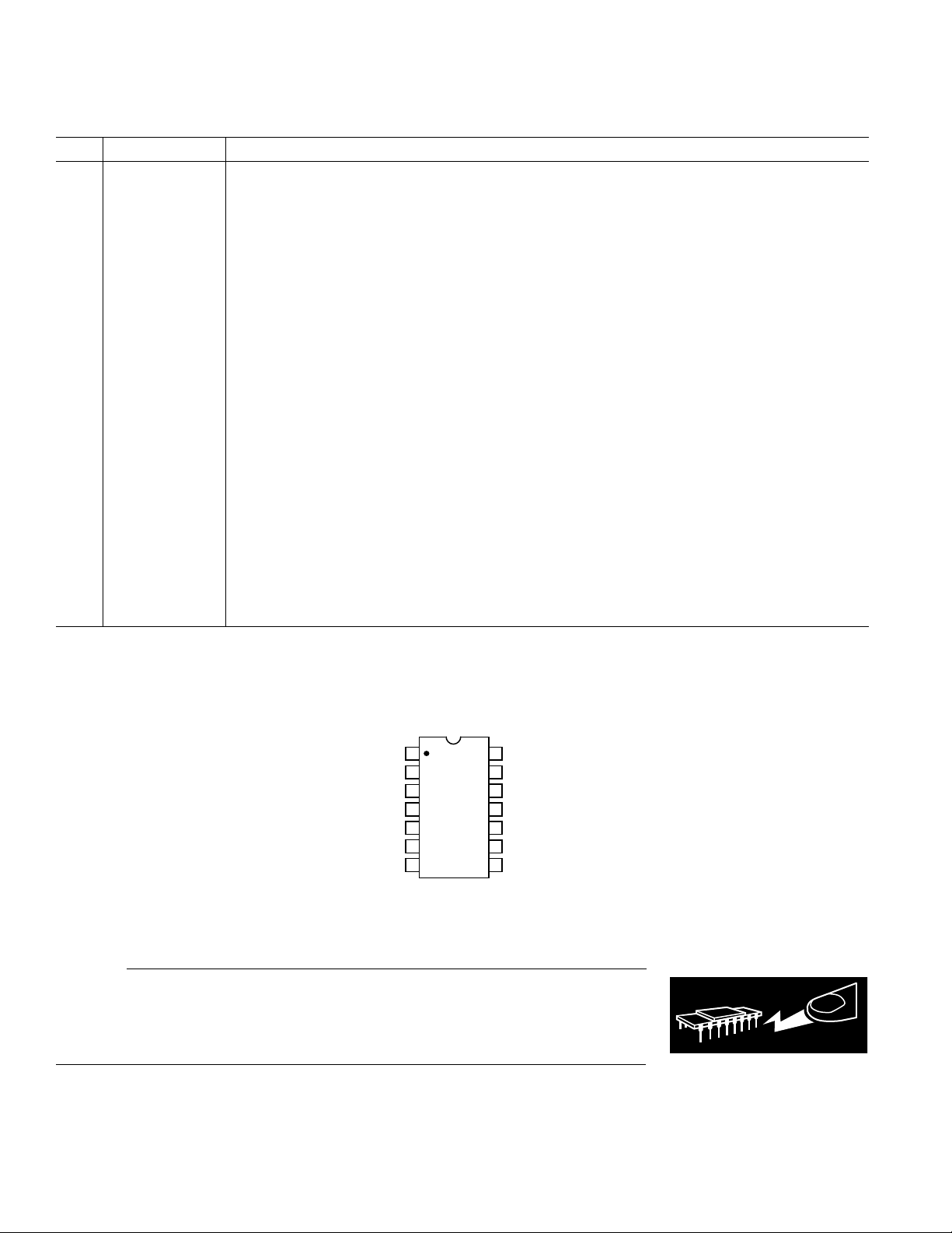
PIN FUNCTION DESCRIPTIONS
Pin # Mnemonic Function
1 P-Channel Drive High Current Gate Drive for Top P-Channel MOSFET. The voltage swing at Pin 4 is from V
ground.
2 NC No Connection.
3V
4C
5 Int V
IN
T
CC
Input Voltage.
External Capacitor CT from Pin 4 to Ground Sets the Operating Frequency. The frequency is also
dependent on the ratio V
OUT/VIN
.
Internal Supply Voltage, Nominally 3.3 V. Must be decoupled to signal ground. Do not externally load
this pin.
6I
TH
Error Amplifier Decoupling Point. The current comparator threshold increases with the Pin 7 voltage.
7 Sense– Connects to internal resistive divider that sets the output voltage in ADP1148-3.3 and ADP1148-5
versions. Pin 7 is also the (–) input for the current comparator.
8 Sense+ The (+) Input for the Current Comparator. A built-in offset between Pins 7 and 8, in conjunction with
, sets the current trip threshold.
R
SENSE
9V
FB
For the ADP1148 adjustable version, Pin 9 serves as the feedback pin from an external resistive divider
used to set the output voltage. On ADP1148-3.3 and ADP1148-5 versions, this pin is not used.
10 Shutdown Taking Pin 10 of the ADP1148, ADP1148-3.3 or ADP1148-5 high holds both MOSFETs off. Must be
at ground potential for normal operation.
11 Signal GND Small Signal Ground. Must be routed separately from other grounds to the (–) terminal of C
12 Power GND Driver Power Ground. Connects to source of N-channel MOSFET and the (–) terminal of C
13 NC No Connection.
14 N-Channel Drive High Current Drive for bottom N-channel MOSFET. The voltage swing at Pin 13 is from ground to
VIN.
IN
OUT
IN
to
.
.
PIN CONFIGURATIONS
14-Lead Plastic DIP
14-Lead Plastic SO
P-DRIVE
SENSE(–)
1
2
NC
3
V
IN
ADP1148
4
C
TOP VIEW
T
(Not to Scale)
5
INT V
CC
6
I
TH
7
NC = NO CONNECT
*FIXED OUTPUT VERSIONS = SD1
N-DRIVE
14
13
NC
12
POWER GND
11
SIGNAL GND
10
SHUTDOWN
9
V
FB
8
SENSE(+)
*
CAUTION
ESD (electrostatic discharge) sensitive device. Electrostatic charges as high as 4000 V readily
accumulate on the human body and test equipment and can discharge without detection. Although
the ADP1148, ADP1148-3.3, ADP1148-5 feature proprietary ESD protection circuitry, permanent
damage may occur on devices subjected to high energy electrostatic discharges. Therefore, proper
ESD precautions are recommended to avoid performance degradation or loss of functionality.
–4–
REV. A

Typical Performance Characteristics–ADP1148, ADP1148-3.3, ADP1148-5
L = 50mH
R
SENSE
= 0.02V
L = 25mH
R
SENSE
= 0.02V
L = 50mH
R
SENSE
= 0.05V
(V
IN–VOUT
) VOLTAGE – V
1000
800
0
052341
600
400
200
C
OUT
– mF
DV
OUT
– mV
V
IN
+40
+20
–60
04 166 8 10 12 14
0
–20
–40
FIGURE 1 CIRCUIT
I
LOAD
= 1A
I
LOAD
= 0.1A
V
SHUTDOWN
= 2V
INPUT VOLTAGE – V
SUPPLY CURRENT – mA
30
0
46 2081012141618
25
20
15
10
5
200
150
– mV
100
SENSE
R
50
0
0
123
MAXIMUM OUTPUT CURRENT – A
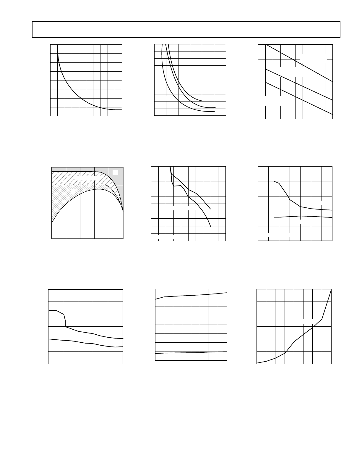
Figure 3. Selecting R
mum Output Current
100
GATE CHARGE
95
90
EFFICIENCY/LOSS – %
85
80
0.01 0.03 3.00.1 0.3 1.0
I
Q
OUTPUT CURRENT – A
SENSE
5
4
vs. Maxi-
I2R
1000
800
600
400
VIN = 7V
CAPACITANCE – pF
200
0
0 300100 200
V
SENSE
V
= 12V
IN
FREQUENCY – kHz
= V
OUT
VIN = 10V
= 5V
Figure 4. Operating Frequency vs.
Timing Capacitor Value
100
98
96
94
92
90
88
86
EFFICIENCY – %
84
82
80
0204 8 12 16
I
= 100mA
LOAD
FIGURE 1 CIRCUIT
INPUT VOLTAGE – V
I
LOAD
= 1A
Figure 5. Selecting Minimum Output
Capacitor vs. (V
IN–VOUT
) and Inductor
Figure 6. Typical Efficiency Losses
60
40
20
– mV
0
OUT
DV
–20
–40
–60
0 0.5 2.51.0 1.5 2.0
Figure 9. Load Regulation
REV. A
FIGURE 1 CIRCUIT
VIN = 6V
VIN = 12V
LOAD CURRENT – A
Figure 7. Efficiency vs. Input Voltage
1.6
1.4
1.2
1.0
0.8
0.6
0.4
SUPPLY CURRENT – mA
0.2
0.0
46 20
ACTIVE MODE
SLEEP MODE
8 1012141618
INPUT VOLTAGE – V
Figure 10. DC Supply Current
–5–
Figure 8. ADP1148-5 Output Voltage
Change vs. Input Voltage
Figure 11. Supply Current in Shutdown
 Loading...