

High Efficiency Synchronous
Q
R
S
V
TH1
V
IN
SENSE(–)
V
TH2
1.25V
OFF-TIME
CONTROL
100kV
13kV
B
V
IN
P-DRIVE SENSE(+) SENSE(–)
G
4 6
C
T
I
TH
SHUTDOWN
8
13
ADP1148
10mV to
150mV
C
V
FB
INT V
CC
REFERENCE
510
T
N-DRIVE
PWR
GND
14
12
ADJUSTABLE
VERSION
V
FB
9
7
S
1
Q
R
S
2
V
SLEEP
SIGNAL
GND
11
NON-OVERLAP
DRIVE
a
ADP1148, ADP1148-3.3, ADP1148-5
FEATURES
Operation From 3.5 V to 18 V Input Voltage
Ultrahigh Efficiency > 95%
Low Shutdown Current
Current Mode Operation for Excellent Line and Load
Transient Response
High Efficiency Maintained Over Wide Current Range
Logic Controlled Micropower Shutdown
Short Circuit Protection
Very Low Dropout Operation
Synchronous FET Switching for High Efficiency
Adaptive Nonoverlap Gate Drives
APPLICATIONS
Notebook and Palmtop Computers
Portable Instruments
Battery Operated Digital Devices
Industrial Power Distribution
Avionics Systems
Telecom Power Supplies
GPS Systems
Cellular Telephones
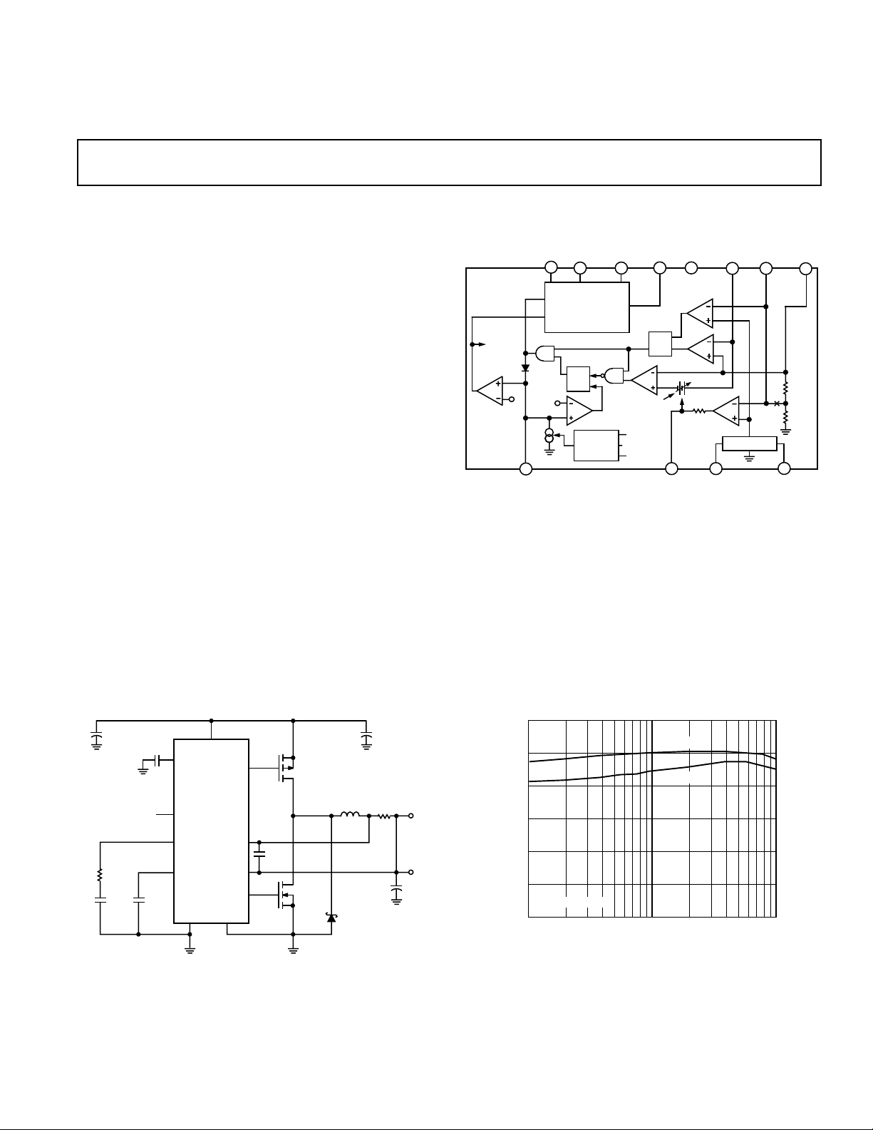
GENERAL DESCRIPTION
The ADP1148 is part of a family of synchronous step-down
switching regulator controllers featuring automatic sleep mode
to maintain high efficiencies at low output currents. These
devices drive external complementary power MOSFETs at
switching frequencies up to 250 kHz using a constant off-time
current-mode architecture.
Step-Down Switching Regulators
FUNCTIONAL BLOCK DIAGRAM
The constant off-time architecture maintains constant ripple
current in the inductor, easing the design of wide input range
converters. Current-mode operation provides excellent line and
load transient response. The operating current level is user
programmable via an external current sense resistor.
The ADP1148 incorporates automatic Power Saving Sleep
Mode operation when load currents drop below the level required for continuous operation. In sleep mode, standby power
is reduced to only about 2 mW at V
both MOSFETs are turned off.
= 10 V. In shutdown,
IN
TYPICAL APPLICATIONS
VIN (5.2V TO 18V)
++
C
100mF
62mH
C1
10BQ040
IN
R
L*
SENSE
0.05V
1mF
>1.5V = SHUTDOWN
R
1kV
C
3300pF
10nF
0V = NORMAL
C
C
T
470pF
C
Figure 1. High Efficiency Step-Down Converter Figure 2. ADP1148-5 Typical Efficiency
REV. A
Information furnished by Analog Devices is believed to be accurate and
reliable. However, no responsibility is assumed by Analog Devices for its
use, nor for any infringements of patents or other rights of third parties
which may result from its use. No license is granted by implication or
otherwise under any patent or patent rights of Analog Devices.
INT V
ADP1148
SHUTDOWN
I
TH
C
T
S-GND
V
IN
CC
P-DRIVE
SENSE(+)
SENSE(–)
N-DRIVE
P-GND
P-CH
IRF7204
1000pF
N-CH
IRF7403
*COILTRONICS CTX-68-4
**KRL SL-1-C1-0R050L
**
V
OUT
5V/2A
+C
390mF
OUT
100
95
90
85
EFFICIENCY – %
80
75
FIGURE 1 CIRCUIT
70
0.02 2
LOAD CURRENT – A
VIN = 6V
VIN = 10V
0.2
One Technology Way, P.O. Box 9106, Norwood, MA 02062-9106, U.S.A.
Tel: 781/329-4700 World Wide Web Site: http://www.analog.com
Fax: 781/326-8703 © Analog Devices, Inc., 1997

ADP1148, ADP1148-3.3, ADP1148-5–SPECIFICATIONS
ELECTRICAL CHARACTERISTICS
(08C ≤ TA ≤ +708C,1 VIN = 10 V, V
Parameter Symbol Conditions
2
= 0 V, unless otherwise noted. See Figure 17.)
SHUTDOWN
Min Typ Max Units
FEEDBACK VOLTAGE
ADP1148 Only V
10
VIN = 9 V 1.21 1.25 1.29 V
FEEDBACK CURRENT
ADP1148 Only I
REGULATED OUTPUT VOLTAGE V
10
OUT
ADP1148-3.3 I
ADP1148-5 I
OUTPUT VOLTAGE LINE T
REGULATION dV
OUT
VIN = 9 V
= 700 mA 3.23 3.33 3.43 V
LOAD
= 700 mA 4.9 5.05 5.2 V
LOAD
= +25°C, VIN = 7 V to 12 V,
A
I
= 50 mA –40 +40 mV
LOAD
0.2 1.0 µA
OUTPUT VOLTAGE LOAD
REGULATION dV
ADP1148-3.3 5 mA < I
ADP1148-5 5 mA < I
SLEEP MODE OUTPUT RIPPLE dV
INPUT DC SUPPLY CURRENT
3
Normal Mode V
Sleep Mode (ADP1148-3.3) V
Sleep Mode (ADP1148-5) V
Shutdown V
OUT
I
OUT
I
Q
= 0 A 50 mV p-p
LOAD
TA = +25°C
= 4 V < VIN < 18 V 1.6 2.3 mA
IN
= 4 V < VIN < 18 V 160 250 µA
IN
= 4 V < VIN < 18 V 160 250 µA
IN
SHUTDOWN
< 2 A 40 65 mV
LOAD
< 2 A 60 100 mV
LOAD
= 2.1 V, 10 20 µA
4 V < VIN < 15 V
CURRENT SENSE THRESHOLD V
VOLTAGE
4
8–V7
ADP1148 Only V
ADP1148-3.3 V
ADP1148-5 V
V9 = V
V7 = 5 V, TA = +25°C25mV
= V
9
= 5 V 130 150 170 mV
V
7
= V
7
= V
V
7
= V
7
V7 = V
/4 + 25 mV (Forced),
OUT
/4 mV – 25 mV (Forced),
OUT
+ 100 mV (Forced) 25 mV
OUT
100 mV (Forced) 130 150 170 mV
OUT –
+ 100 mV (Forced 25 mV
OUT
– 100 mV (Forced) 130 150 170 mV
OUT
SHUTDOWN PIN THRESHOLD
ADP1148-3.3, ADP1148-5 V
SHUTDOWN PIN INPUT CURRENT I
PIN DISCHARGE CURRENT I
C
T
OFF-TIME t
DRIVER OUTPUT TRANSITION t
10
10
4
OFF
, t
R
F
TA = +25°C 0.6 0.8 2.0 V
0 V < V
SHUTDOWN
TA = +25°C, V
= V
V
7
V
OUT
, 506590 µA
OUT
= 0 V 2 10 µA
CT = 390 pF, I
< 8 V, VIN = 18 V 1.2 5 µA
in Regulation,
OUT
= 700 mA 4 5 6 µs
LOAD
CL = 3000 pF (Pins 1, 14)
TIMES VIN = 6 V, TA = +25°C 100 200 ns
NOTES
1
All limits at temperature extremes are guaranteed via correlation using standard Quality Control methods. Specifications subject to change without notice.
2
TJ is calculated from the ambient temperature TA and power dissipation PD according to the following formulas:
ADP1148AR, ADP1148AR-3.3, ADP1148AR-5: TJ = TA + (PD × 110°C/W)
ADP1148AN, ADP1148AN-3.3, ADP1148AN-5: TJ = TA + (PD × 70°C/W)
3
Dynamic supply current is higher due to the gate charge being delivered at the switching frequency. The allowable operating frequency may be limited by power
dissipation at high input voltages.
4
The ADP1148 version is tested with external feedback resistors, setting the nominal output voltage to 3.3 V.
Specifications subject to change without notice.
–2–
REV. A

ADP1148, ADP1148-3.3, ADP1148-5
ELECTRICAL CHARACTERISTICS
Parameter Symbol Conditions
(–408C ≤ TA ≤ +858C,1 VIN = 10 V, V
2
= 0 V, unless otherwise noted. See Figure 17.)
SHUTDOWN
Min Typ Max Units
FEEDBACK VOLTAGE
ADP1148 Only V
REGULATED OUTPUT VOLTAGE V
10
OUT
ADP1148-3.3 I
ADP1148-5 I
INPUT DC SUPPLY CURRENT
3
I
Q
VIN = 9 V 1.20 1.25 1.30 V
VIN = 9 V
= 700 mA 3.17 3.33 3.4 V
LOAD
= 700 mA 4.85 5.05 5.2 V
LOAD
Normal Mode VIN = 4 V < VIN < 18 V 1.6 2.6 mA
Sleep Mode (ADP1148-3) V
Sleep Mode (ADP1148-5) V
Shutdown V
= 4 V < VIN < 18 V 160 280 µA
IN
= 6 V < VIN < 18 V 160 280 µA
IN
SHUTDOWN
= 2.1 V, 10 24 µA
4 V < VIN < 12 V
CURRENT SENSE THRESHOLD
VOLTAGE
ADP1148 Only V9 = V
ADP1148-3.3 V
ADP1148-5.0 V
SHUTDOWN PIN THRESHOLD V
4
V8–V
10
7
= 5 V
V
7
= V
V
9
= 5 V
V
7
= V
7
= V
V
7
= V
7
V7 = V
/4 + 25 mV (Forced), 0 mV
OUT
/4 – 25 mV (Forced), 115 150 175 mV
OUT
+ 100 mV (Forced) 0 mV
OUT
– 100 mV (Forced) 115 150 175 mV
OUT
+ 100 mV (Forced) 0 mV
OUT
– 100 mV (Forced) 115 150 175 mV
OUT
ADP1148-3.3, ADP1148-5 0.55 0.8 2 V
OFF-TIME t
NOTES
1
All limits at temperature extremes are guaranteed via correlation using standard Quality Control method.
2
TJ is calculated from the ambient temperature TA and power dissipation PD according to the following formulas:
ADP1148AR, ADP1148AR-3, ADP1148AR-5: TJ = TA + (PD × 110°C/W)
ADP1148AN, ADP1148AN-3, ADP1148AN-5: TJ = TA + (PD × 70°C/W)
3
Dynamic supply current is higher due to the gate charge being delivered at the switching frequency. The allowable operating frequency may be limited by power
dissipation at high input voltages.
4
The ADP1148 version is tested with external feedback resistors setting the nominal output voltage to 3.3 V.
Specifications subject to change without notice.
OFF
CT = 390 pF, I
= 700 mA 4 5 6.2 µs
LOAD
ABSOLUTE MAXIMUM RATINGS
Input Supply Voltage (Pin 3) . . . . . . . . . . . . . –0.3 V to +20 V
Continuous Output Currents (Pins 1, 14) . . . . . . . . . . 50 mA
Sense Voltages (Pins 7, 8) . . . . . . . . . . . . . . . . –0.3 V to V
CC
Operating Temperature Range . . . . . . . . . . . . 0°C to +70°C
Extended Commercial Temperature Range . . –40°C to +85°C
Junction Temperature . . . . . . . . . . . . . . . . . . . . . . . . . 150°C
Storage Temperature Range . . . . . . . . . . . . –65°C to +150°C
Lead Temperature (Soldering, 10 sec) . . . . . . . . . . . . 300°C
REV. A
ORDERING GUIDE
Output Package Package
Model Voltage Description Option
ADP1148AN ADJ Plastic DIP N-14
ADP1148AR ADJ Small Outline Package SO-14
ADP1148AN-3.3 3.3 V Plastic DIP N-14
ADP1148AR-3.3 3.3 V Small Outline Package SO-14
ADP1148AN-5 5 V Plastic DIP N-14
ADP1148AR-5 5 V Small Outline Package SO-14
–3–
ADP1148, ADP1148-3.3, ADP1148-5
WARNING!
ESD SENSITIVE DEVICE
PIN FUNCTION DESCRIPTIONS
Pin # Mnemonic Function
1 P-Channel Drive High Current Gate Drive for Top P-Channel MOSFET. The voltage swing at Pin 4 is from V
ground.
2 NC No Connection.
3V
4C
5 Int V
IN
T
CC
Input Voltage.
External Capacitor CT from Pin 4 to Ground Sets the Operating Frequency. The frequency is also
dependent on the ratio V
OUT/VIN
.
Internal Supply Voltage, Nominally 3.3 V. Must be decoupled to signal ground. Do not externally load
this pin.
6I
TH
Error Amplifier Decoupling Point. The current comparator threshold increases with the Pin 7 voltage.
7 Sense– Connects to internal resistive divider that sets the output voltage in ADP1148-3.3 and ADP1148-5
versions. Pin 7 is also the (–) input for the current comparator.
8 Sense+ The (+) Input for the Current Comparator. A built-in offset between Pins 7 and 8, in conjunction with
, sets the current trip threshold.
R
SENSE
9V
FB
For the ADP1148 adjustable version, Pin 9 serves as the feedback pin from an external resistive divider
used to set the output voltage. On ADP1148-3.3 and ADP1148-5 versions, this pin is not used.
10 Shutdown Taking Pin 10 of the ADP1148, ADP1148-3.3 or ADP1148-5 high holds both MOSFETs off. Must be
at ground potential for normal operation.
11 Signal GND Small Signal Ground. Must be routed separately from other grounds to the (–) terminal of C
12 Power GND Driver Power Ground. Connects to source of N-channel MOSFET and the (–) terminal of C
13 NC No Connection.
14 N-Channel Drive High Current Drive for bottom N-channel MOSFET. The voltage swing at Pin 13 is from ground to
VIN.
IN
OUT
IN
to
.
.
PIN CONFIGURATIONS
14-Lead Plastic DIP
14-Lead Plastic SO
P-DRIVE
SENSE(–)
1
2
NC
3
V
IN
ADP1148
4
C
TOP VIEW
T
(Not to Scale)
5
INT V
CC
6
I
TH
7
NC = NO CONNECT
*FIXED OUTPUT VERSIONS = SD1
N-DRIVE
14
13
NC
12
POWER GND
11
SIGNAL GND
10
SHUTDOWN
9
V
FB
8
SENSE(+)
*
CAUTION
ESD (electrostatic discharge) sensitive device. Electrostatic charges as high as 4000 V readily
accumulate on the human body and test equipment and can discharge without detection. Although
the ADP1148, ADP1148-3.3, ADP1148-5 feature proprietary ESD protection circuitry, permanent
damage may occur on devices subjected to high energy electrostatic discharges. Therefore, proper
ESD precautions are recommended to avoid performance degradation or loss of functionality.
–4–
REV. A
Typical Performance Characteristics–ADP1148, ADP1148-3.3, ADP1148-5
L = 50mH
R
SENSE
= 0.02V
L = 25mH
R
SENSE
= 0.02V
L = 50mH
R
SENSE
= 0.05V
(V
IN–VOUT
) VOLTAGE – V
1000
800
0
052341
600
400
200
C
OUT
– mF
DV
OUT
– mV
V
IN
+40
+20
–60
04 166 8 10 12 14
0
–20
–40
FIGURE 1 CIRCUIT
I
LOAD
= 1A
I
LOAD
= 0.1A
V
SHUTDOWN
= 2V
INPUT VOLTAGE – V
SUPPLY CURRENT – mA
30
0
46 2081012141618
25
20
15
10
5
200
150
– mV
100
SENSE
R
50
0
0
123
MAXIMUM OUTPUT CURRENT – A
Figure 3. Selecting R
mum Output Current
100
GATE CHARGE
95
90
EFFICIENCY/LOSS – %
85
80
0.01 0.03 3.00.1 0.3 1.0
I
Q
OUTPUT CURRENT – A
SENSE
5
4
vs. Maxi-
I2R
1000
800
600
400
VIN = 7V
CAPACITANCE – pF
200
0
0 300100 200
V
SENSE
V
= 12V
IN
FREQUENCY – kHz
= V
OUT
VIN = 10V
= 5V
Figure 4. Operating Frequency vs.
Timing Capacitor Value
100
98
96
94
92
90
88
86
EFFICIENCY – %
84
82
80
0204 8 12 16
I
= 100mA
LOAD
FIGURE 1 CIRCUIT
INPUT VOLTAGE – V
I
LOAD
= 1A
Figure 5. Selecting Minimum Output
Capacitor vs. (V
IN–VOUT
) and Inductor
Figure 6. Typical Efficiency Losses
60
40
20
– mV
0
OUT
DV
–20
–40
–60
0 0.5 2.51.0 1.5 2.0
Figure 9. Load Regulation
REV. A
FIGURE 1 CIRCUIT
VIN = 6V
VIN = 12V
LOAD CURRENT – A
Figure 7. Efficiency vs. Input Voltage
1.6
1.4
1.2
1.0
0.8
0.6
0.4
SUPPLY CURRENT – mA
0.2
0.0
46 20
ACTIVE MODE
SLEEP MODE
8 1012141618
INPUT VOLTAGE – V
Figure 10. DC Supply Current
–5–
Figure 8. ADP1148-5 Output Voltage
Change vs. Input Voltage
Figure 11. Supply Current in Shutdown

OUTPUT VOLTAGE – V
OFF TIME – msec
80
30
0
0.3 0.5 5.01.0 1.5 2.0 2.5 3.0 3.3 3.5 4.0 4.5
70
40
20
10
60
50
5V
3.3V
ADP1148, ADP1148-3.3, ADP1148-5–Typical Performance Characteristics
1.8
1.6
1.4
1.2
1.0
0.8
0.6
0.4
NORMALIZED FREQUENCY
0.2
0.0
12
(VIN–V
08C
OUT
708C
) – V
258C
1246810
Figure 12. Operating Frequency vs.
(V
IN–VOUT
SENSE VOLTAGE – mV
)
155
150
145
MAXIMUM THRESHOLD
140
135
130
125
30
25
20
15
10
5
GATE CHARGE CURRENT – mA
0
20 50 260
Qn+Qp = 100nC
Qn+Qp = 50nC
80 110 140 170 200 230
OPERATING FREQUENCY – kHz
Figure 13. Gate Charge Supply
Current
Figure 14. Off Time vs. V
OUT
120
0
25 70
TEMPERATURE – 8C
Figure 15. Current Sense Threshold
Voltage
100
85
–6–
REV. A

ADP1148, ADP1148-3.3, ADP1148-5
APPLICATIONS
The ADP1148 uses a current-mode, constant off-time structure
to switch a pair of external complementary N- and P-channel
MOSFETs. The operating frequency of the device is determined by the value of the external capacitor connected to the
pin.
C
T
The output voltage is sensed by an internal voltage divider which is
connected to the Sense(–) pin (ADP1148-3.3 and AD1148-5) or
an external voltage divider returned to V
(ADP1148). A voltage
FB
comparator V, and a gain block G compare the values of the
divided output voltage with a reference voltage of 1.25 V.
To maximize the efficiency, the ADP1148 automatically switches
between two operational modes, power-saving and continuous.
The Flip-Flop 1 is the main control element when the device is
in its power-saving mode while the gain block is the main control when the output voltage moves to continuous mode. During
the continuous mode of the PMOS switch on-cycle, the current
comparator C, monitors the voltage between Sense(–) and
Sense(+). When the voltage level reaches the threshold level, the
P drive output is switched to V
MOSFET. The timing capacitor C
which turns off the P-channel
IN
is now able to discharge at
T
a rate determined by the off-time controller. The discharge
current is made to be proportional to the value of the output
voltage (measured at the Sense(–) pin) to model the inductor
current which decays at a rate which is proportional to the output voltage. While the timing capacitor is discharging, the N
drive output goes to V
, turning on the N-channel MOSFET.
IN
When the voltage level on the timing capacitor has discharged to
the threshold voltage level V
, comparator T switches setting
TH1
Flip-Flop 1. This forces the N drive to go off and the P drive
output low and subsequently turns the P-channel MOSFET on.
The sequence is then repeated. As load current increases, the
output voltage starts to reduce. This results in the output of the
gain circuit increasing the level of the current comparator threshold, thus tracking the load current.
At very low load currents the power-saving sequence will be
interrupted by the Set of Flip-Flop 2, by voltage comparator B,
which also monitors the voltage across R
. When the load
SENSE
current decreases to half the designed inductor ripple current,
the voltage across R
will reverse polarity. When this hap-
SENSE
pens, comparator B will set the Q-bar output of Flip-Flop 2,
which will go to logic zero state and interrupt the cycle-by-cycle
operation and inhibit the output FET-driver. The output of the
power supply storage capacitor will slowly be drained by the
load and the output voltage starts decreasing. When this
decreased voltage exceeds the V
of comparator V, this in turn
OS
will reset Flip-Flop 2, and normal cycle-by-cycle operation will
resume. If the load is very small, it will take a long time for FlipFlop 2 to reset, and during that time the oscillator capacitor
may discharge below V
capacitor discharges below V
. At the point at which the timing
TH2
, comparator S trips causing the
TH2
internal sleep-bar to go low. The circuit is now in sleep mode
and the N-channel Power MOSFET remains turned off. While
the circuit remains in this mode, a significant amount of the
circuit of the IC is turned off dropping the ground current from
approximately 1.6 mA to a level of 160 µA. In this state the load
current is supplied by the output capacitor. The sleep mode is
also terminated by the reset of Flip-Flop 2.
To prevent both the external MOSFETs from ever being turned
on simultaneously, feedback is incorporated to sense the state of
the driver output pins.
Before the N drive output can go high, the P drive output must
also be high. Likewise, the P drive output is unable to go low
while the N drive output is high. By utilizing a constant off-time
structure, the device operation is a function of the input voltage.
To limit the effect of frequency variation as the device approaches
dropout, the controller begins to increase the discharge current
drops below V
as V
IN
+1.5 V. While the device is in drop-
OUT
out, the P-channel MOSFET is on constantly.
R
Selection For Output Current
SENSE
The choice of R
is based on the required output current.
SENSE
The ADP1148 current comparator has a threshold range which
extends from 0 mV to a maximum of 150 mV/R
SENSE
. The
current comparator threshold sets the peak of the inductor current, yielding a maximum output current I
equal to the peak
MAX
value less half the peak-to-peak ripple current. The ADP1148
operates effectively with values of R
200 mΩ. A graph for selecting R
SENSE
current is given in Figure 3. Solving for R
from 20 mΩ to
SENSE
versus maximum output
and allowing a
SENSE
margin for variations in the ADP1148 and external component
values yields:
= 100 mV/I
R
SENSE
The peak short circuit current, (I
has been chosen, I
R
SENSE
can be predicted from the fol-
SC(PK)
SC(PK)
MAX
) tracks I
MAX
. Once
lowing equation:
= 150 mV/R
I
SC(PK)
SENSE
The load current, below which power-saving mode commences
(I
POWER-SAVING
) is determined by the offset in comparator B and
the value of the inductor chosen. Comparator B is designed to
have approximately 5 mV offset. This offset and the inductor
can now be used to predict the power saving mode current as
follows:
I
POWER-SAVING
~ 5 mV/R
The ADP1148 automatically extends t
SENSE
+ VO × t
during a short circuit
OFF
OFF
/2 L
to provide adequate time for the inductor current to decay between switch cycles. The resulting ripple current causes the
average short circuit current, I
mately I
MAX
.
, to be lowered to approxi-
SC(AVG)
L and CT Selection for Operating Frequency
The ADP1148 uses a constant off-time architecture with t
OFF
determined by an external timing capacitor CT. Each time the
P-channel MOSFET switch turns on, the voltage on C
to approximately 3.3 V. During the off time, C
a current which is proportional to V
. The voltage on CT is
OUT
is discharged by
T
is reset
T
analogous to the current in inductor L, which likewise decays at
a rate proportional to V
. Therefore, the inductor value must
OUT
track the timing capacitor value.
The value of C
is calculated from the preferred continuous
T
mode operating frequency:
= 1/2.6 × 104 × f
C
T
Assumes V
= 2 V
IN
A graph for selecting C
(Figure 1 circuit).
OUT
versus frequency including the effects
T
of input voltage is given in Figure 5.
*Component, voltage, current, etc., values are in SI-units (international standard)
unless otherwise indicated.
REV. A
–7–

ADP1148, ADP1148-3.3, ADP1148-5
As the operating frequency is increased, the gate charge losses
will cause reduced efficiency (see Efficiency section). The full
formula for operating frequency is given by:
f = ( 1 – V
where t
V
REG
= 1.3 × 10⁴ × CT × V
OFF
is the desired output voltage (i.e., 5 V or 3.3 V), V
the measured output voltage. Thus, V
Note that as V
reduces, the frequency also decreases. When
IN
OUT/VIN
REG/VOUT.
REG/VOUT
)/t
OFF
= 1 in regulation.
OUT
is
the input to output voltage differential drops below 1.5 V, the
ADP1148 reduces t
. This prevents audible operation before the device goes into
C
T
by increasing the discharge current in
OFF
dropout.
Once the frequency has been set by C
chosen to provide no more than 25 mV/R
, the inductor L must be
T
of peak-to-peak
SENSE
inductor ripple current. This is set by the equation:
25 mV
R
SENSE
V
OUT×tOFF
=
L
MIN
or
25 mV
× R
SENSE
Substituting for t
V
L
OFF
MIN
OUT×tOFF
=
from above gives the minimum required
inductor value of:
= 5.1 × 10⁵ × R
L
MIN
SENSE
× CT × V
REG
As the inductor value increases above the minimum value, the
ESR requirements for the output capacitor are relaxed at the
expense of efficiency. If too small an inductor is used, the inductor current will decrease past zero and change polarity. A result
of this occurrence will be that the ADP1148 may not be in
power saving mode operation and efficiency will be significantly
reduced at low currents.
Inductor Core
Once the minimum value for L is known, the selection of the
inductor must be made. High efficiency converters -π generally
cannot accommodate the core loss found in low cost powdered
iron cores, forcing the use of more expensive ferrite, molypermalloy
(MPP), or Kool Mµ
®
cores. Actual core loss is independent of
core size for a fixed inductor value, but it is very dependent on
inductance selected. As inductance increases, core losses decrease. Unfortunately, increased inductance requires more turns
of wire and therefore copper losses will increase.
Ferrite designs have very low core loss, so design goals can focus
on copper loss and preventing saturation. Ferrite core material
saturates “hard,” which causes the inductance to collapse
abruptly when the peak design current is exceeded. This results
in a sharp increase in inductor ripple current and subsequently
output voltage ripple which can cause the power saving mode
operation to be falsely triggered in the ADP1148. To prevent
this action from occurring, do not allow the core to saturate!
Molypermalloy from Magnetics, Inc., is a very good, low loss
core material for toroids, but it is more expensive than ferrite. A
reasonable compromise from the same manufacturer is Kool
Mµ. Toroids are very space efficient, especially when you can
use several layers of wire. Because they generally lack a bobbin,
mounting is more difficult. Many new designs for surface mount
All trademarks are the property of their respective holders.
components are also available from Coiltronics which do not
increase the component height significantly.
Power MOSFET
Two external power MOSFETs must be selected for use with
the ADP1148, a P-channel MOSFET for the main switch, and
an N-channel MOSFET for the synchronous switch. The main
selection parameters for the power MOSFETs are the threshold
voltage V
and on resistance R
GS(TH)
DS(ON)
.
The minimum input voltage dictates whether standard threshold
or logic-level threshold MOSFETs must be used. For V
standard threshold MOSFETs (V
is expected to drop below 8 V, logic-level threshold MOSFETs
V
IN
(V
< 2.5 V) are strongly recommended. When logic-level
GS(TH)
) < 4 V) may be used. If
GS(TH
> 8 V,
IN
MOSFETs are used, the ADP1148 supply voltage must be less
than the absolute maximum V
rating for the MOSFETs (e.g.,
GS
>±8 V of IRF7304.
The maximum output current I
determines the R
MAX
DS(ON)
requirement for the two power MOSFETs. When the ADP1148
is operating in continuous mode, the simplifying assumption can
be made that one of the two MOSFETs is always conducting
the average load current. The duty cycles for the MOSFET and
diode are given by:
P-Channel Duty Cycle = V
N-Channel Duty Cycle = (VIN – V
From the duty cycle the required R
OUT/VIN
OUT
for each MOSFET
DS(ON)
)/V
IN
can be derived:
P-Ch
N-Ch
RDS(ON)
where P
d
and PN are the allowable power dissipations and dp and
p
are the temperature dependency of R
N
= (VIN × PP)/[V
RDS(ON)
= (VIN × PN)/[(VIN – V
OUT
× I
OUT
DS(ON)
MAX
) × I
2
× (1 + dP)]
2
× (1+dN)]
MAX
. PP and PN will
be determined by efficiency and/or thermal requirements (see
Efficiency). (1+d) is generally given for a MOSFET in the form
of a normalized R
vs. temperature curve, but d = 0.007/°C
DS(ON)
can be used as an approximation for low voltage MOSFETs.
The Schottky diode D1 shown in Figure 1 conducts only during
the deadtime between the conduction of the two power
MOSFETs. D1’s purpose is to prevent the body-diode of the
N-channel MOSFET from turning on and storing charge during
the dead time, which could cost as much as 1% in efficiency. D1
should be selected for forward voltage of less than 0.5 V when
conducting I
CIN and C
MAX
Selection
OUT
.
In continuous mode, the source current of the P-channel
MOSFET is a square wave of duty cycle V
OUT/VlN
. To prevent
large voltage transients, a low ESR input capacitor sized for the
maximum rms current must be used. The maximum rms capacitor current is given by:
required I
C
IN
This formula has a maximum at V
/2. This simple worst case condition is commonly used for
I
OUT
RMS
~ [V
OUT(VIN
IN
– V
= 2 V
OUT
OUT
0.5
)]
× I
, where I
MAX/VIN
RMS
=
design because even significant deviations do not offer much
relief. Note that capacitor manufacturer’s ripple current ratings
are often based on only 2000 hours of life. This makes it advisable to further derate the capacitor, or to choose a capacitor
rated at a higher temperature than required. Several capacitors
may also be paralleled to meet size or height requirements in the
design. Always consult the manufacturer if there is any question.
–8–
REV. A

ADP1148, ADP1148-3.3, ADP1148-5
An additional 0.1 µF – 1 µF ceramic bypass capacitor is advised
Pin 3 parallel with CIN. The selection of C
on V
IN
is driven
OUT
by the required effective series resistance (ESR). The ESR of
must be less than twice the value of R
C
OUT
SENSE
for proper
operation of the ADP1148:
required ESR < 2 R
C
OUT
SENSE.
Optimum efficiency is obtained by making the ESR equal to
. As the ESR is increased up to 2 R
R
SENSE
, the efficiency
SENSE
degrades by less than 1%.
Manufacturers such as Sprague, and United Chemmicon should
be considered for high performance capacitors. The OS-CON
semiconductor dielectric capacitor has the lowest ESR for its
size, at a somewhat higher price. Once the ESR requirement for
has been met, the RMS current rating generally far ex-
C
OUT
ceeds the I
RIPPLE(P-P)
requirement.
In surface-mount applications multiple capacitors may have to
be paralleled to meet the capacitance, ESR, or RMS current
handling requirements of the application. Aluminum electrolytic
and dry tantalum capacitors are both available in surface-mount
configurations. In the case of tantalum, it is critical that the
capacitors are surge tested for use in switching power supplies.
Consult the manufacturer for other specific recommendations.
The C
output filter capacitor has to be sized correctly to avoid
O
excessive ripple voltages at low frequencies. See Figure 5 for
output capacitor selection.
Transient Response
The regulator loop response can be checked by looking at the
load transient response. Switching regulators take several cycles
to respond to a step in dc (resistive) load current. When a load
step occurs, V
where ESR is the effective series resistance of C
also begins to charge or discharge C
adapts to the current change and returns V
state value. During this recovery time V
shifts by an amount equal to D1
OUT
until the regulator loop
OUT
OUT
can be monitored
OUT
OUT. D1LOAD
to its steady-
LOAD
× ESR
,
for overshoot or ringing which would indicate a stability problem. The external components on the I
pin shown in the
TH
Figure 1 circuit will prove adequate compensation for most
applications.
A second, more severe transient is caused by switching in loads
with large (>1 mF) supply bypass capacitors. The discharged
bypass capacitors are effectively put in parallel with C
ing a rapid drop in V
. No regulator can deliver enough cur-
OUT
OUT
, caus-
rent to prevent this problem if the load switch resistance is low
and it is driven quickly. The only solution is to limit the inrush
current to these capacitors below the current limit of the circuit.
Efficiency
The percent efficiency of a switching regulator is equal to the
output power divided by the input power times 100%. It is often
useful to analyze individual losses to determine what is limiting
the efficiency and which change would produce the most improvement. Percent efficiency can be expressed as:
% Efficiency = 100% - (L1 + L2 + L3 +. . . )
where L1, L2, etc. are the individual losses as a percentage of
input power. (For high efficiency circuits only small errors are
incurred by expressing losses as a percentage of output power.)
Although all dissipative elements in the circuit produce losses,
three main sources usually account for most of the losses in
ADP1148 circuits:
1) ADP1148 dc bias current,
2) MOSFET gate charge currents,
2
× R losses.
3) I
1) The dc supply current is the current which flows into V
3 less the gate charge current. For V
= 10 V the ADP1148
IN
IN
Pin
dc supply current is 160 µA for no load, and increases pro-
portionally with load up to a constant 1.6 mA after the
ADP1148 has entered continuous mode. Because the dc bias
current is drawn from V
input voltage. For V
, the resulting loss increases with
IN
= 10 V the dc bias losses are generally
IN
less than 1% for load currents over 30 mA. However, at very
low load currents the dc bias current accounts for nearly all
of the loss.
2) MOSFET gate charge currents result from switching the gate
capacitance of the power MOSFETs. Each time a MOSFET
gate is switched from low to high to low again, a packet of
charge dQ moves from V
a current out of V
IN
dc supply current. In continuous mode, I
). The typical gate charge for a 100 mΩ N-channel power
Q
N
to ground. The resulting dQ/dt is
IN
which is typically much larger than the
GATECHG
= f (QP +
MOSFET is 25 nC and for the P-channel about twice that
value. This results in I
GATECHG
= 7.5 mA in 100 kHz continu-
ous operation for a 2% to 3% typical midcurrent loss with
= 10 V.
V
IN
Note that the gate charge loss increases directly with both
input voltage and operating frequency. This is the principal
reason why the highest efficiency circuits operate at moderate
frequencies. Furthermore, it argues against using a larger
MOSFET than necessary to control I
2
× R losses are easily predicted from the dc resistances of
3) I
2
× R losses.
the MOSFET, inductor, and current shunt. In continuous
mode the average output current flows through L and
, but is “chopped” between the P-channel and N-
R
SENSE
channel MOSFETs. If the two MOSFETs have about the
same R
summed with the resistances of L and R
losses. For example, if each R
and R
This results in losses ranging from 3% to 10% as the output
current increases from 0.5 A to 2 A. I
, the resistance of one MOSFET can be simply
DS(ON)
= 100 mΩ, RL = 150 mΩ,
= 50 mΩ, then the total resistance is 300 mΩ .
SENSE
DS(ON)
to obtain I2 × R
SENSE
2
× R losses cause the
efficiency to roll-off at high output currents.
Figure 6 shows how the efficiency losses in a typical ADP1148
regulator. The gate charge loss is responsible for the majority of
the efficiency lost in the midcurrent region. If power saving
mode operation was not employed at low currents, the gate
charge loss alone would cause the efficiency to drop to unacceptable levels. With power saving mode operation, the dc supply
current represents the lone (and unavoidable) loss component
which continues to become a higher percentage as output current is reduced. As expected, the I
load currents. Other losses including C
2
× R losses dominate at high
IN
and C
ESR dissi-
OUT
pative losses, MOSFET switching losses, Schottky conduction
losses during deadtime and inductor core losses, generally
account for less than 2% total additional loss.
REV. A
–9–

ADP1148, ADP1148-3.3, ADP1148-5
ADP1148
INT V
CC
C
T
5
4
VN2222LL
*FROM CROWBAR
DETECT CIRCUIT
*ACTIVE WHEN V
GATE
= VIN
OFF WHEN V
GATE
= GROUND
Design Example
As a design example, assume V
I
MAX
ately be calculated:
Assume that the MOSFET dissipations are to be limited to
P
N
If T
50°C/W, then the junction temperatures will be 63°C and d
= 0.007 × (63–25) = 0.27.
d
P
The required R
The P-channel requirement can be met by a IRF7204. The
N-channel requirement can be met by a IRF7404. Note that
the most stringent requirement for the N-channel MOSFET is
with V
circuit, the worst case N-channel MOSFET dissipation rises to:
With the 50 mΩ sense resistor I
ing the N-channel dissipation to 0.45 W at die temperature of
73°C.
C
IN
ture, and C
efficiency.
Now allow V
voltages, the operating frequency will decrease and the Pchannel will be conducting most of the time causing the power
dissipation to increase. At V
to:
f
MIN =
and the P-channel power dissipation increases to:
This last step is needed to ensure the maximum temperature of
the P-channel MOSFET is not exceeded.
ADP1148 Adjustable Applications
When an output voltage other than 3.3 V or 5 V is required, the
ADP1148 adjustable version is used with an external resistive
divider from V
mined by:
To prevent a stray pickup, a 100 pF capacitor is suggested across
R1 located close to the ADP1148.
Auxiliary Windings
The ADP1148 synchronous switch removes the normal limitation that power must be drawn from the inductor primary winding in order to extract power from auxiliary windings. With
synchronous switching, auxiliary outputs may be loaded without
regard to the primary output load, providing that the loop remains in continuous mode operation.
= 2 A, and f = 200 kHz, R
R
SENSE
t
= (1/200 kHz) × [1 – (5/12)] = 2.92 µs
OFF
= 2.92 µs/(1.3 × 104) = 220 pF
C
T
5
L min = 5.1 × 10
× 50 E-3 Ω × 220 pF × 5 V = 28 µH
IN
SENSE
= 100 mV/2 = 50 m
= 12 V (nominal), V
. CT, and L can immedi-
Ω
OUT
= 5 V,
= 2PP = 250 mW.
= 50°C and the thermal resistance of each MOSFET is
A
for each MOSFET can now be calculated:
DS(ON)
P-Ch R
N-Ch R
= 0 (i.e., short circuit). During a continuous short
OUT
= 12 × 0.25/5 × 2 × 1.27 = 120 m
DS(ON)
= 12 × 0.25/7 × 2 × 1.27 = 85 m
DS(ON)
SC(AVG)
2
× R
× (1 + dN)
DS(ON)
= 2 A will result, increas-
SC(AVG)
~ I
P
N
=
P
Ω
Ω
will require an rms current rating of at least 1 A at tempera-
will require an ESR of 50 mΩ for optimum
OUT
to drop to its minimum value. At lower input
IN
= 7 V, the frequency shifts
IN(MIN)
(1 – V
= (120 mΩ) (2 A)2 (1.27) 5 V/7 V = 435 mW
P
P
OUT
)/t
OUT/VIN
= (1/2.92 µs) × (1 – 5/7) = 98 kHz
OFF
to VFB Pin 9. The regulated voltage is deter-
= 1.25 (1 + R2/R1)
V
OUT
–10–
Output Crowbar
An added feature to using an N-channel MOSFET as the synchronous switch is the ability to crowbar the output with the
same MOSFET. Pulling the timing cap C
pin above 1.5 V
T
when the output voltage is greater than the desired regulated
value will turn “on” the N-channel MOSFET and turn “off” the
P-channel MOSFET.
A fault condition such as an external short between V
, or an internal short of the P-channel device which causes
V
OUT
IN
and
the output voltage to go above a maximum allowable value can
be detected by external circuity. Turning on the N-channel
MOSFET when this fault is detected will cause large currents to
flow and blow the system fuse.
The N-channel MOSFET needs to be sized so it will safely
handle this over current condition. The typical delay from pulling the C
pin high and the N drive, Pin 14 going high is 250 ns.
T
Note: under shutdown conditions, the N-channel MOSFET
is held OFF and pulling the C
pin high will not cause the
T
N-channel MOSFET to crowbar the output.
A simple N-channel FET can be used as an interface between
the overvoltage detect circuitry and the ADP1148 as shown in
Figure 16.
Figure 16. Output Crowbar Interface
Troubleshooting
Since efficiency is critical to ADP1148 applications, it is very
important to verify that the circuit is functioning correctly in
both continuous and power saving mode operation. The waveform to monitor is the voltage on the timing capacitor
pin.
C
T
In continuous mode (I
on the C
pin should be a sawtooth with a 0.9 V p-p swing. This
T
LOAD
> I
POWER SAVING MODE
), the voltage
voltage should never dip below 2 V as shown in Figure 17a.
When load currents are low (I
LOAD
< I
POWER SAVING MODE),
saving mode operation occurs. The voltage on the C
power
pin now
T
falls to ground for periods of time as shown in Figure 17b. If the
pin is observed falling to ground at high output currents, it
C
T
indicates poor decoupling or improper grounding. Refer to the
Board Layout list.
3.3V
(A) CONTINOUS MODE OPERATION
(B) POWER-SAVING MODE
0V
3.3V
0V
Figure 17. CT Waveforms
REV. A

ADP1148, ADP1148-3.3, ADP1148-5
Board Layout
When laying out the printed circuit board, the following check
list should be used to ensure proper operation of the ADP1148.
These items are also illustrated graphically in the layout diagram
of Figure 18. Check the following in your layout:
1) Are the signal and power grounds segregated? The ADP1148
SIGNAL GND (Pin 11) must return to the (–) plate of C
OUT
.
The power ground returns to the source of the N-channel
MOSFET, anode of the Schottky diode, and (–) plate of C
,
IN
which should have as short lead lengths as possible.
2) Does the ADP1148 SENSE(–), (Pin 7), connect to a point
close to R
and the (+) plate Of C
SENSE
? In adjustable
OUT
versions the resistive divider R1, R2 must be connected between the (+) plate of C
and signal ground.
OUT
3) Are the SENSE(–) and SENSE(+) leads routed together with
minimum PC trace spacing? The 1000 pF capacitor between
Pins 7 and 8 should be as close as possible to the ADP1148.
P-CHANNEL
1
P-DRIVE
2
NC
1mF
C
T
10nF
3300pF
1kV
3
V
4
C
5
INT V
6
I
7
SENSE(–)
IN
T
CC
TH
ADP1148
POWER GND
SIGNAL GND
SHUTDOWN
SENSE(+)
N-DRIVE
V
NC
14
13
12
11
10
9
FB
8
4) Does the (+) plate of C
connect to the source of the
IN
P-channel MOSFET as closely as possible? This capacitor
provides the ac current to the P-channel MOSFET.
5) Is the input decoupling capacitor (1 µF) connected closely
between V
(Pin 3) and POWER GND (Pin 12)? This
IN
capacitor carries the MOSFET driver peak currents.
6) Is INTV
(Pin 5) decoupled with a 10 nF capacitor to
CC
signal ground?
7) Is the SHUTDOWN (Pin 10) actively pulled to ground
during normal operation? The Shutdown pin is high impedance and must not be allowed to float.
To prevent noise spikes from erroneously tripping the current
comparator, a 1000 pF capacitor is needed across Sense(–) and
Sense(+).
C
D1
N-CHANNEL
IN
R1
R2
C
OUT
L
R
SENSE
V
IN
–
–
V
OUT
REV. A
1000pF
NC = NO CONNECT
R1, R2 OUTPUT DIVIDER REQUIRED
FOR ADJUSTABLE VERSION ONLY.
Figure 18. ADP1148 Layout Diagram (See Board Layout)
–11–

ADP1148, ADP1148-3.3, ADP1148-5
IRF7204
D1
10BQ040
IRF7403
V
IN
4V TO 18V
C
100mF
20V
IN
N-DRIVE
NC
V
14
13
12
11
10
9
FB
8
1000pF
50mH
*L
**R
SENSE
0.1V
300pF
1
P-DRIVE
2
1mF
C
T
10nF
C
C
3300pF
R
C
1kV
NC
ADP1148-3.3
3
V
4
C
5
INT V
6
I
TH
7
SENSE(–)
IN
T
POWER GND
SIGNAL GND
SHUTDOWN
CC
NC = NO CONNECT
*COILTRONICS CTX50-2-MP
**KRL SP-1/2-A1-0R100J
SENSE(+)
Figure 19. ADP1148 Low Dropout, 3.3 V/1 A High Efficiency Regulator
V
IN
4V TO 9V
560pF
IRF7204
1
P-DRIVE
2
ADP1148
1mF
C
T
10nF
C
C
6800pF
R
C
1kV
NC
3
V
IN
4
C
T
5
INT V
6
I
TH
7
SENSE(–)
POWER GND
SIGNAL GND
SHUTDOWN
CC
NC = NO CONNECT
*COILTRONICS CTX50-2-MP
**KRL SL-1-C1-0R05J
SENSE(+)
N-DRIVE
NC
V
14
13
12
11
10
9
FB
8
50mH
1000pF
D1
10BQ015
IRF7403
*L
25kV
200pF
1%
**R
SENSE
0.05V
75kV
1%
Figure 20. 4 V to 9 V Input Voltage to –5 V/1.4 A Regulator
C
OUT
220mF
10V 3 2
AVX
C
IN
220mF
20V
V
OUT
3.3V/1A
V
OUT
–5V/1.4A
C
OUT
220mF 3 2
10V
–12–
REV. A

ADP1148, ADP1148-3.3, ADP1148-5
V
IN
5.2V TO 14V
C
IRF7204
D1
10BQ040
IRF7403
IN
100mF
20V
N-DRIVE
NC
V
14
13
*L
50mH
12
11
R1B
10
9
FB
8
**R
1000pF
0.05V
100pF
SENSE
R1A
33kV
1%
43kV
1%
R2
56kV
1%
390pF
1
P-DRIVE
2
ADP1148
1mF
C
T
10nF
C
C
3300pF
R
1kV
NC
3
V
IN
4
C
T
5
INT V
6
I
TH
7
SENSE(–)
C
POWER GND
SIGNAL GND
SHUTDOWN
CC
SENSE(+)
NC = NO CONNECT
*COILTRONICS CTX50-2-MP
**KRL SL-1-C1-0R050J
Figure 21. Logic Selectable 5 V/1 A or 3.3 V/2 A High Efficiency Regulator
VN2222LL
0V: V
5V: V
C
OUT
220mF
10V 3 2
OS-CON
V
3.3V/2A
OR 5V/2A
OUT
OUT
OUT
= 3.3V
= 5V
REV. A
–13–

ADP1148, ADP1148-3.3, ADP1148-5
OUTLINE DIMENSIONS
Dimensions shown in inches and (mm).
0.795 (20.19)
0.725 (18.42)
14
17
PIN 1
0.210 (5.33)
MAX
0.160 (4.06)
0.115 (2.93)
0.022 (0.558)
0.014 (0.356)
0.3444 (8.75)
0.3367 (8.55)
14-Lead Plastic DIP
(N-14)
8
0.280 (7.11)
0.240 (6.10)
0.060 (1.52)
0.015 (0.38)
0.130
(3.30)
MIN
0.100
(2.54)
BSC
0.070 (1.77)
0.045 (1.15)
SEATING
PLANE
14-Lead Plastic SO
(SO-14)
0.325 (8.25)
0.300 (7.62)
0.015 (0.381)
0.008 (0.204)
0.195 (4.95)
0.115 (2.93)
0.1574 (4.00)
0.1497 (3.80)
0.0098 (0.25)
0.0040 (0.10)
SEATING
PLANE
14 8
PIN 1
0.0500
0.0192 (0.49)
(1.27)
0.0138 (0.35)
BSC
0.2440 (6.20)
71
0.2284 (5.80)
0.0688 (1.75)
0.0532 (1.35)
0.0099 (0.25)
0.0075 (0.19)
0.0196 (0.50)
0.0099 (0.25)
8°
0°
0.0500 (1.27)
0.0160 (0.41)
x 45°
–14–
REV. A

–15–

C2219a–2–12/97
–16–
PRINTED IN U.S.A.
 Loading...