Analog Devices ADP1111 Datasheet

Micropower, Step-Up/Step-Down SW
DRIVER
I
LIM
SW1
SW2
V
IN
GND
SET
A0
GAIN BLOCK/
ERROR AMP
COMPARATOR
A1
A2
FB
1.25V
REFERENCE
OSCILLATOR
ADP1111
DRIVER
I
LIM
SW1
SW2
V
IN
GND
SET
A0
GAIN BLOCK/
ERROR AMP
COMPARATOR
A1
A2
SENSE
1.25V
REFERENCE
OSCILLATOR
ADP1111-5
ADP1111-12
R1 R2 220k
a
Regulator; Adjustable and Fixed 3.3 V, 5 V, 12 V
FEATURES
Operates from 2 V to 30 V Input Voltage Range
72 kHz Frequency Operation
Utilizes Surface Mount Inductors
Very Few External Components Required
Operates in Step-Up/Step-Down or Inverting Mode
Low Battery Detector
User Adjustable Current Limit
Internal 1 A Power Switch
Fixed or Adjustable Output Voltage
8-Pin DIP or SO-8 Package
APPLICATIONS
3 V to 5 V, 5 V to 12 V Step-Up Converters
9 V to 5 V, 12 V to 5 V Step-Down Converters
Laptop and Palmtop Computers
Cellular Telephones
Flash Memory VPP Generators
Remote Controls
Peripherals and Add-On Cards
Battery Backup Supplies
Uninterruptible Supplies
Portable Instruments
ADP1111
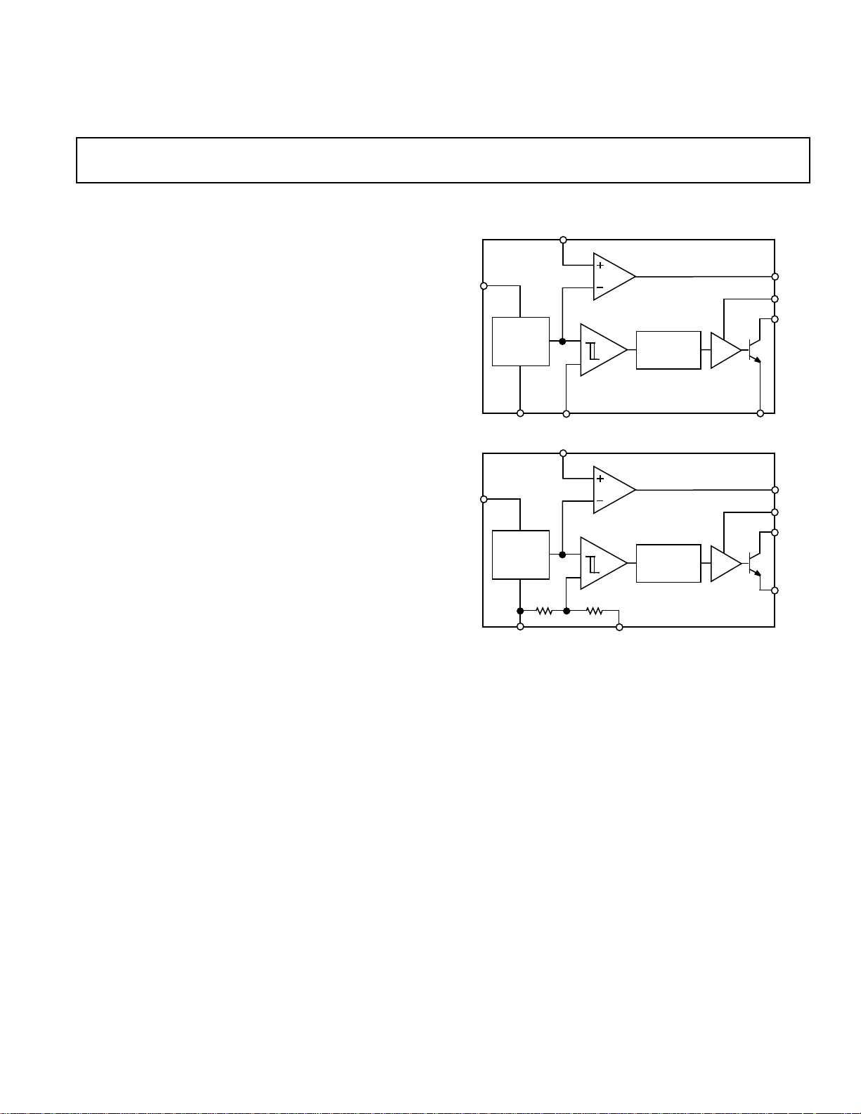
FUNCTIONAL BLOCK DIAGRAMS
GENERAL DESCRIPTION
The ADP1111 is part of a family of step-up/step-down switching regulators that operates from an input voltage supply of 2 V
to 12 V in step-up mode and up to 30 V in step-down mode.
The ADP1111 can be programmed to operate in step-up/stepdown or inverting applications with only 3 external components.
The fixed outputs are 3.3 V, 5 V and 12 V; and an adjustable
version is also available. The ADP1111 can deliver 100 mA at
5 V from a 3 V input in step-up mode, or it can deliver 200 mA
at 5 V from a 12 V input in step-down mode.
REV. 0
Information furnished by Analog Devices is believed to be accurate and
reliable. However, no responsibility is assumed by Analog Devices for its
use, nor for any infringements of patents or other rights of third parties
which may result from its use. No license is granted by implication or
otherwise under any patent or patent rights of Analog Devices.
Maximum switch current can be programmed with a single
resistor, and an open collector gain block can be arranged in
multiple configuration for low battery detection, as a post linear
regulator, undervoltage lockout, or as an error amplifier.
If input voltages are lower than 2 V, see the ADP1110.
One Technology Way, P.O. Box 9106, Norwood, MA 02062-9106, U.S.A.
Tel: 617/329-4700 World Wide Web Site: http://www.analog.com
Fax: 617/326-8703 © Analog Devices, Inc., 1996

ADP1111–SPECIFICATIONS
(08C ≤ TA ≤ +708C, VIN = 3 V unless otherwise noted)
Parameter Conditions V
QUIESCENT CURRENT Switch Off I
INPUT VOLTAGE Step-Up Mode V
S
Q
IN
Min Typ Max Units
300 500 µA
2.0 12.6 V
Step-Down Mode 30.0 V
COMPARATOR TRIP POINT
VOLTAGE ADP1111
OUTPUT SENSE VOLTAGE ADP1111-3.3 V
ADP1111-5
ADP1111-12
1
2
2
OUT
1.20 1.25 1.30 V
3.13 3.30 3.47 V
4.75 5.00 5.25 V
11.40 12.00 12.60 V
COMPARATOR HYSTERESIS ADP1111 8 12.5 mV
OUTPUT HYSTERESIS ADP1111-3.3 21 50 mV
ADP1111-5 32 50 mV
ADP1111-12 75 120 mV
OSCILLATOR FREQUENCY f
OSC
54 72 88 kHz
DUTY CYCLE Full Load DC 43 50 65 %
SWITCH ON TIME I
SW SATURATION VOLTAGE T
STEP-UP MODE V
Tied to V
LIM
= +25°C
A
= 3.0 V, ISW = 650 mA V
IN
V
= 5.0 V, ISW = 1 A 0.8 1.0 V
IN
IN
t
ON
SAT
57 9 µs
0.5 0.65 V
STEP-DOWN MODE VIN = 12 V, ISW = 650 mA 1.1 1.5 V
FEEDBACK PIN BIAS CURRENT ADP1111 VFB = 0 V I
SET PIN BIAS CURRENT V
GAIN BLOCK OUTPUT LOW I
REFERENCE LINE REGULATION 5 V ≤ V
= V
SET
REF
= 300 µA
SINK
V
= 1.00 V V
SET
≤ 30 V 0.02 0.075 %/V
IN
I
FB
SET
OL
160 300 nA
270 400 nA
0.15 0.4 V
2 V ≤ VIN ≤ 5 V 0.4 %/V
GAIN BLOCK GAIN R
CURRENT LIMIT T
= 100 kΩ
L
= +25°C
A
220 Ω from I
3
LIM
to V
A
V
IN
I
LIM
1000 6000 V/V
400 mA
CURRENT LIMIT TEMPERATURE
COEFFICIENT –0.3 %/°C
SWITCH OFF LEAKAGE CURRENT T
= +25°C
A
Measured at SW1 Pin
V
= 12 V 1 10 µA
SW1
MAXIMUM EXCURSION BELOW GND T
NOTES
1
This specification guarantees that both the high and low trip points of the comparator fall within the 1.20 V to 1.30 V range.
2
The output voltage waveform will exhibit a sawtooth shape due to the comparator hysteresis. The output voltage on the fixed output versions will always be within
the specified range.
3
100 kΩ resistor connected between a 5 V source and the AO pin.
4
All limits at temperature extremes are guaranteed via correlation using standard statistical methods.
Specifications subject to change without notice.
= +25°C
A
I
≤ 10 µA, Switch Off –400 –350 mV
SW1
–2–
REV. 0

ADP1111
WARNING!
ESD SENSITIVE DEVICE
ABSOLUTE MAXIMUM RATINGS
Supply Voltage . . . . . . . . . . . . . . . . . . . . . . . . . . . . . . . . . 36 V
SW1 Pin Voltage . . . . . . . . . . . . . . . . . . . . . . . . . . . . . . . 50 V
SW2 Pin Voltage . . . . . . . . . . . . . . . . . . . . . . . . –0.5 V to V
IN
Feedback Pin Voltage (ADP1111) . . . . . . . . . . . . . . . . . 5.5 V
Switch Current . . . . . . . . . . . . . . . . . . . . . . . . . . . . . . . 1.5 A
Maximum Power Dissipation . . . . . . . . . . . . . . . . . . 500 mW
Operating Temperature Range
ADP1111A . . . . . . . . . . . . . . . . . . . . . . . . . . . 0°C to +70°C
Storage Temperature Range . . . . . . . . . . . . . –65°C to 150°C
Lead Temperature (Soldering, 10 sec) . . . . . . . . . . . . . 300°C
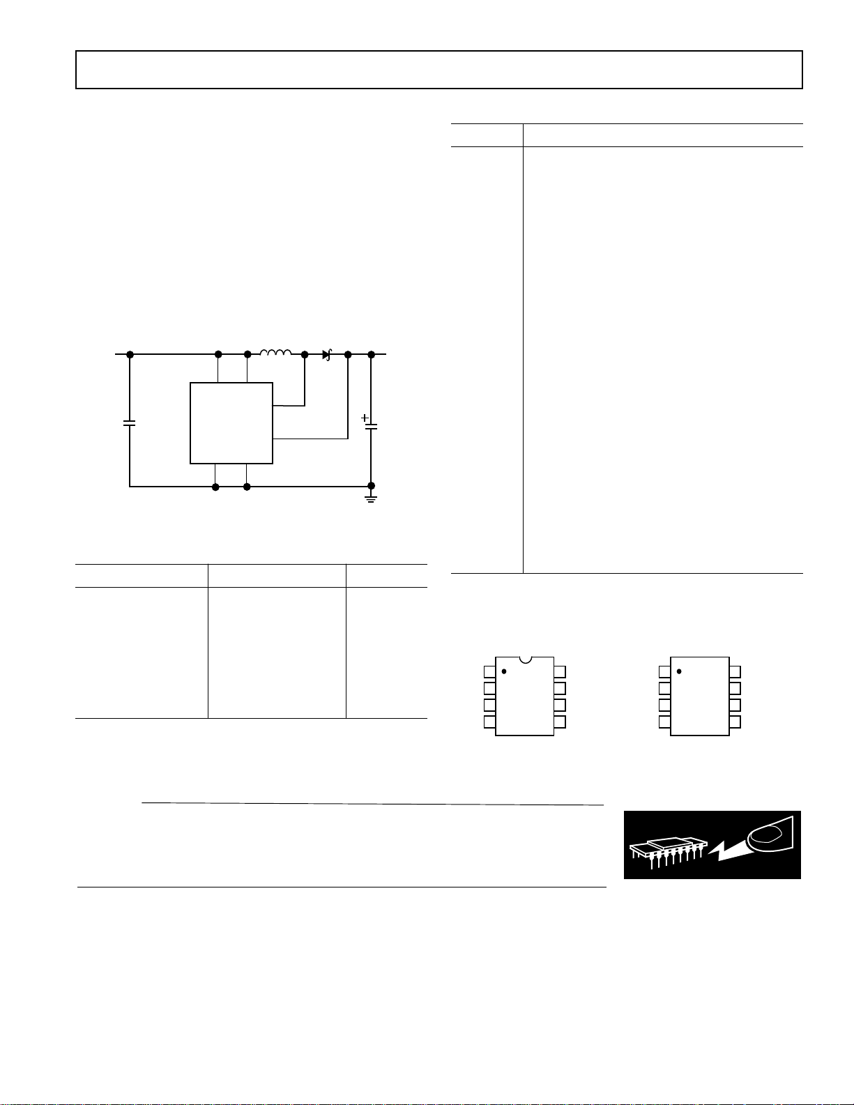
TYPICAL APPLICATION
SUMIDA
CD54-220K
22µH
INPUT
3V
10µF
(OPTIONAL)
I
LIMVIN
SW1
ADP1111AR-5
SENSE
SW2GND
MBRS120T3
5V
100mA
33µF
Figure 1. 3 V to 5 V Step-Up Converter
ORDERING GUIDE
Model Output Voltage Package*
ADP1111AN ADJ N-8
ADP1111AR ADJ SO-8
ADP1111AN-3.3 3.3 V N-8
ADP1111AR-3.3 3.3 V SO-8
ADP1111AN-5 5 V N-8
ADP1111AR-5 5 V SO-8
ADP1111AN-12 12 V N-8
ADP1111AR-12 12 V SO-8
*N = Plastic DIP, SO = Small Outline Package.
PIN DESCRIPTIONS
Mnemonic Function
I
LIM
For normal conditions this pin is connected to
V
. When lower current is required, a resistor
IN
should be connected between I
and VIN.
LIM
Limiting the switch current to 400 mA is achieved
by connecting a 220 Ω resistor.
V
IN
Input Voltage.
SW1 Collector Node of Power Transistor. For step-
down configuration, connect to V
. For step-up
IN
configuration, connect to an inductor/diode.
SW2 Emitter Node of Power Transistor. For step-
down configuration, connect to inductor/diode.
For step-up configuration, connect to ground.
Do not allow this pin to go more than a diode
drop below ground.
GND Ground.
AO Auxiliary Gain (GB) Output. The open collector
can sink 300 µA. It can be left open if unused.
SET Gain Amplifier Input. The amplifier’s positive
input is connected to SET pin and its negative
input is connected to the 1.25 V reference. It can
be left open if unused.
FB/SENSE On the ADP1111 (adjustable) version this pin
is connected to the comparator input. On the
ADP1111-3.3, ADP1111-5 and ADP1111-12,
the pin goes directly to the internal application
resistor that sets output voltage.
PIN CONFIGURATIONS
8-Lead Plastic DIP 8-Lead SOIC
(N-8) (SO-8)
1
I
LIM
ADP1111
2
V
IN
TOP VIEW
3
SW1
(Not to Scale)
SW2
4
*FIXED VERSIONS
8
FB (SENSE)*
7
SET
6
A0
5
GND
1
I
LIM
ADP1111
2
V
IN
TOP VIEW
3
SW1
(Not to Scale)
SW2
4
*FIXED VERSIONS
8
FB (SENSE)*
7
SET
6
A0
5
GND
CAUTION
ESD (electrostatic discharge) sensitive device. Electrostatic charges as high as 4000 V readily
accumulate on the human body and test equipment and can discharge without detection.
Although the ADP1111 features proprietary ESD protection circuitry, permanent damage may
occur on devices subjected to high energy electrostatic discharges. Therefore, proper ESD
precautions are recommended to avoid performance degradation or loss of functionality.
REV. 0
–3–

ADP1111–Typical Characteristics
76
71
67
2304 6 8 10121518212427
75
72
70
69
74
73
INPUT VOLTAGE – V
OSCILLATOR FREQUENCY – kHz
OSCILLATOR FREQUENCY
68
R
LIM
– Ω
1.9
1.7
0.1
1 100010 100
1.5
1.3
0.5
1.1
0.9
0.7
0.3
SWITCH CURRENT – A
STEP-DOWN WITH
V
IN
= 12V
STEP-UP WITH
2V < V
IN
< 5V
OSCILLATOR FREQUENCY – kHz
TEMPERATURE – 8C
80
70
60
–40 8525
64
62
68
66
OSCILLATOR FREQUENCY
70
0
78
72
76
74
1.4
1.2
1.0
0.8
V
= 5V
0.6
0.4
SATURATION VOLTAGE – V
0.2
0
0.1 0.2 0.4 0.6 0.8 1.0 1.2
IN
I
SWITCH
V
= 2V
IN
CURRENT – A
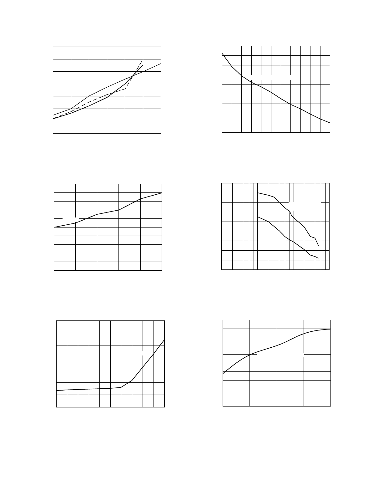
Figure 2. Saturation Voltage vs. I
V
IN
SWITCH
Step-Up Mode
2.0
1.8
1.6
1.4
1.2
V
= 12V
IN
1.0
0.8
ON VOLTAGE – V
0.6
0.4
0.2
0
0.1 0.2 0.4 0.6 0.8 0.9
I
SWITCH
CURRENT – A
= 3V
Current in
Figure 5. Oscillator Frequency vs. Input Voltage
Figure 3. Switch ON Voltage vs. I
Step-Down Mode
1400
1200
1000
800
600
400
QUIESCENT CURRENT – µA
200
0
1.5 303 6 9 12 15 18 21 24 27
Figure 4. Quiescent Current vs. Input Voltage
INPUT VOLTAGE – V
Current In
SWITCH
QUIESCENT CURRENT
–4–
Figure 6. Maximum Switch Current vs. R
LIM
Figure 7. Oscillator Frequency vs. Temperature
REV. 0

7.5
TEMPERATURE – 8C
1.10
1.05
0.80
–40 8525
1.00
0.85
V
IN
= 12V @ ISW = 0.65A
ON VOLTAGE – V
0.95
0.90
070
TEMPERATURE – 8C
250
0
–40 8525
150
100
50
200
BIAS CURRENT
BIAS CURRENT – µA
070
7.4
7.3
7.2
7.1
7.0
ON TIME – µs
6.9
6.8
6.7
6.6
–40 8525
ON TIME
070
ADP1111
TEMPERATURE – 8C
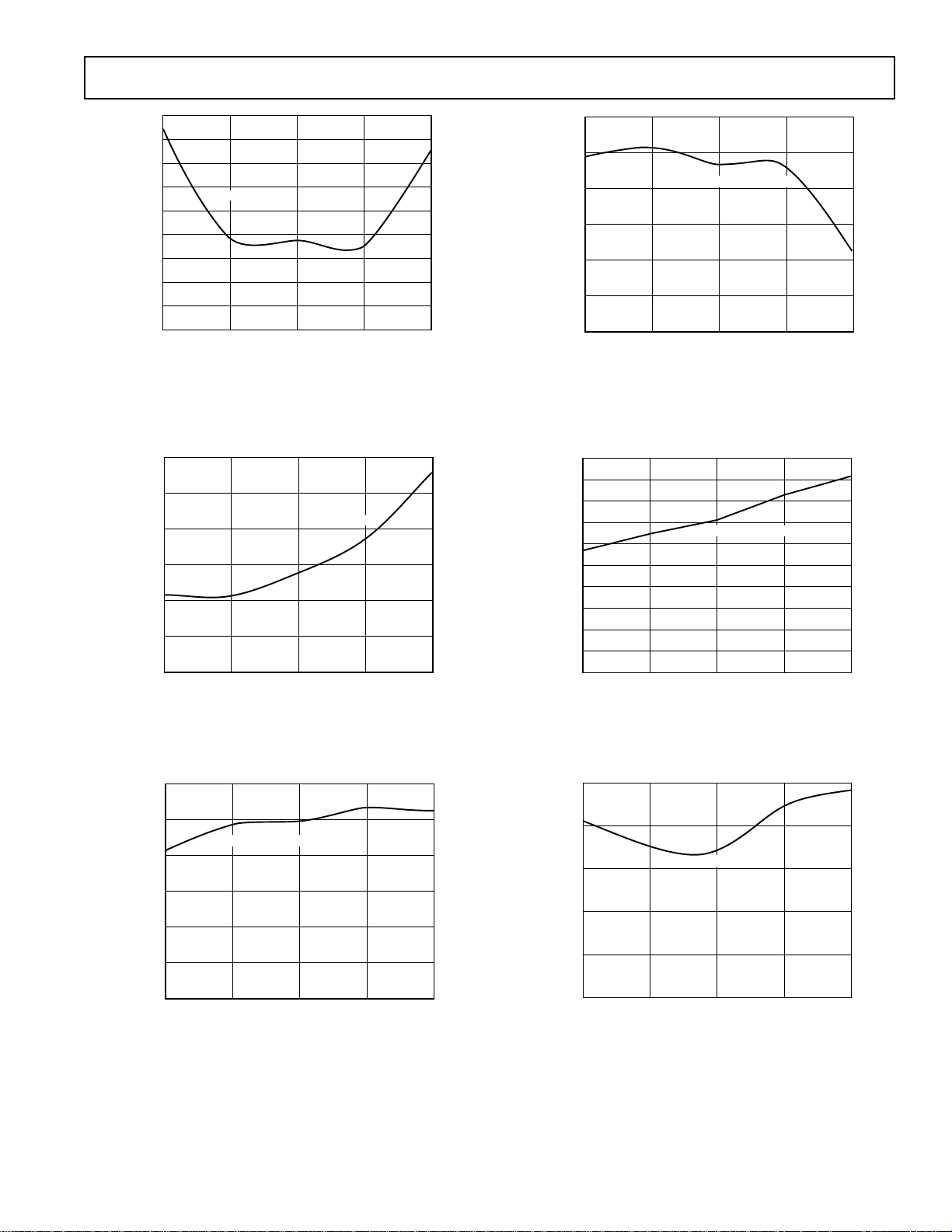
Figure 8. Switch ON Time vs. Temperature
58
56
54
52
DUTY CYCLE – %
50
48
46
–40 8525
070
TEMPERATURE – 8C
DUTY CYCLE
Figure 9. Duty Cycle vs. Temperature
0.6
0.5
V
= 3V @ ISW = 0.65A
0.4
IN
Figure 11. Switch ON Voltage vs. Temperature in StepDown Mode
500
450
400
350
300
250
200
150
QUIESCENT CURRENT – µA
100
50
0
–40 8525
070
QUIESCENT CURRENT
TEMPERATURE – 8C
Figure 12. Quiescent Current vs. Temperature
Figure 10. Saturation Voltage vs. Temperature in Step-Up
Mode
REV. 0
0.3
0.2
SATURATION VOLTAGE – V
0.1
0
–40 8525
070
TEMPERATURE – 8C
Figure 13. Feedback Bias Current vs. Temperature
–5–
 Loading...