

Analog Devices ADP1109AAR-5, ADP1109AAR-3.3, ADP1109AAR-12, ADP1109AAR, ADP1109AAN-5 Datasheet
...
Micropower Low Cost
120kHz
OSCILLATOR
ADP1109A-3.3: R1 = 152kV
ADP1109A-5: R1 = 83kV
ADP1109A-12: R1 = 29kV
V
IN
SENSE
SW
PGND
SHUTDOWN
GND
1.25V
REFERENCE
R2
250kV
R1
DRIVER
COMPARATOR
Q1
A1
120kHz
OSCILLATOR
ADP1109A
V
IN
FB
SW
PGND
SHUTDOWN
GND
1.25V
REFERENCE
DRIVER
COMPARATOR
Q1
A1
Fixed 3.3 V , 5 V, 12 V and Adjustable
a
FEATURES
Operates at Supply Voltages 2 V to 9 V
Fixed 3.3 V, 5 V, 12 V and Adjustable Output
Minimum External Components Required
Ground Current: 460 mA
Oscillator Frequency: 120 kHz
Logic Shutdown
8-Lead DIP and SO-8 Packages
APPLICATIONS
Cellular Telephones
Single-Cell to 5 V Converters
Laptop and Palmtop Computers
Pagers
Cameras
Battery Backup Supplies
Portable Instruments
Laser Diode Drivers
Hand-Held Inventory Computers
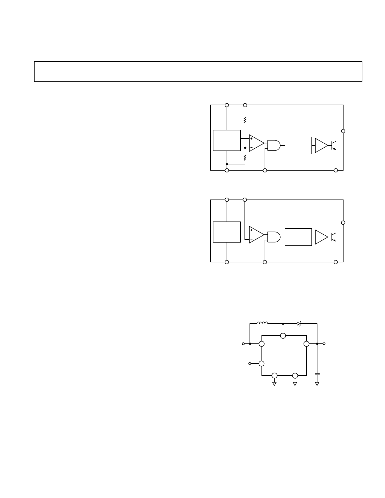
DC-to-DC Converter
ADP1109A
FUNCTIONAL BLOCK DIAGRAM
GENERAL DESCRIPTION
The ADP1109A is a versatile step-up switching regulator. The
device requires only minimal external components to operate as
a complete switching regulator.
The ADP1109A-5 can deliver 100 mA at 5 V from a 3 V input
and the ADP1109A-12 can deliver 60 mA at 12 V from a 5 V
input. The device also features a logic controlled shutdown
capability that, when a logic low is applied, will shut down the
oscillator. The 120 kHz operating frequency allows for the use
of small surface mount components.
The gated oscillator capability eliminates the need for frequency
compensation.
TYPICAL APPLICATION
L1
33mH
3
V
IN
5V
7
SHUTDOWN/PROGRAM
SW
V
IN
ADP1109A-12
SHUTDOWN
PGND GND
4
Flash Memory VPP Generator
D1
SENSE
5
81
V
OUT
12V
60mA
C1
+
22mF
16V
REV. 0
Information furnished by Analog Devices is believed to be accurate and
reliable. However, no responsibility is assumed by Analog Devices for its
use, nor for any infringements of patents or other rights of third parties
which may result from its use. No license is granted by implication or
otherwise under any patent or patent rights of Analog Devices.
One Technology Way, P.O. Box 9106, Norwood, MA 02062-9106, U.S.A.
Tel: 781/329-4700 World Wide Web Site: http://www.analog.com
Fax: 781/326-8703 © Analog Devices, Inc., 1997

ADP1109A–SPECIFICA TIONS
(08C ≤ TA ≤ 708C, VIN = 3 V unless otherwise noted)
Parameter Conditions V
QUIESCENT CURRENT Switch Off I
INPUT VOLTAGE V
S
Q
IN
Min Typ Max Units
460 580 µA
29V
COMPARATOR TRIP POINT
VOLTAGE 1.20 1.25 1.30 V
COMPARATOR HYSTERESIS ADP1109A 8 12.5 mV
OUTPUT VOLTAGE
ADP1109A-3.3 2 V ≤ V
ADP1109A-5 2 V ≤ V
ADP1109A-12 2 V ≤ V
≤ 3 V V
IN
≤ 5 V 4.75 5.00 5.25 V
IN
≤ 9 V 11.45 12.00 12.55 V
IN
OUT
3.13 3.30 3.47 V
OUTPUT VOLTAGE RIPPLE ADP1109A-3.3 15 35 mV
ADP1109A-5 25 50 mV
ADP1109A-12 60 120 mV
OSCILLATOR FREQUENCY f
OSC
95 120 155 kHz
DUTY CYCLE Full Load DC 57 67 77 %
SWITCH-ON TIME t
SWITCH SATURATION VOLTAGE I
= 500 mA V
SW
ON
CESAT
3.8 5.6 7.4 µs
ADP1109A-3.3 VIN = 3 V 0.4 0.8 V
ADP1109A-5 V
= 3 V 0.4 0.8 V
IN
ADP1109A-12 VIN = 3 V 0.4 0.8 V
SWITCH LEAKAGE CURRENT VSW = 9 V, TA = +25°C110µA
SHUTDOWN PIN HIGH V
SHUTDOWN PIN LOW V
SHUTDOWN PIN INPUT CURRENT V
SHUTDOWN PIN INPUT CURRENT V
NOTES
All limits at temperature extremes are guaranteed via correlation using standard quality control methods.
Specifications subject to change without notice.
SHUTDOWN
SHUTDOWN
= 4 V I
= 0 V I
IH
IL
IH
IL
2.0 V
0.8 V
10 µA
20 µA
ABSOLUTE MAXIMUM RATINGS*
Supply Voltage, V
. . . . . . . . . . . . . . . . . . . . –0.4 V to 20 V
OUT
SW Pin Voltage . . . . . . . . . . . . . . . . . . . . . . . . –0.4 V to 50 V
Shutdown Pin Voltage . . . . . . . . . . . . . . . . . . . . . . . . . . 6.0 V
Switch Current . . . . . . . . . . . . . . . . . . . . . . . . . . . . . . . 1.2 A
Maximum Power Dissipation . . . . . . . . . . . . . . . . . . 300 mW
Operating Temperature Range . . . . . . . . . . . . 0°C to +70°C
Storage Temperature Range . . . . . . . . . . . . –65°C to +150°C
Lead Temperature (Soldering, 10 sec) . . . . . . . . . . . +300°C
*This is a stress rating only; operation beyond these limits can cause the device to
be permanently damaged.
–2–
REV. 0
ADP1109A
WARNING!
ESD SENSITIVE DEVICE
PIN FUNCTION DESCRIPTIONS
Pin Mnemonic Function
1V
IN
Input Supply Voltage.
2 NC No Connection.
3 SW Collector Node of Power Transistor.
4 PGND Power Ground.
5 GND Ground.
6 NC No Connection.
7 SHUTDOWN When logic low is applied to this pin,
oscillator is shut down.
8 FB(SENSE) On the ADP1109A (Adjustable), this
pin goes directly to the comparator input.
On the ADP1109A-3.3, ADP1109A-5
and ADP1109A-12, this pin is connected
through the internal resistor that sets
the output voltage.
ORDERING GUIDE
Output Package Package
Model Voltage Description Options
ADP1109AAN ADJ Plastic DIP N-8
ADP1109AAR ADJ Small Outline IC SO-8
ADP1109AAN-3.3 3.3 V Plastic DIP N-8
ADP1109AAR-3.3 3.3 V Small Outline IC SO-8
ADP1109AAN-5 5 V Plastic DIP N-8
ADP1109AAR-5 5 V Small Outline IC SO-8
ADP1109AAN-12 12 V Plastic DIP N-8
ADP1109AAR-12 12 V Small Outline IC SO-8
PIN CONFIGURATIONS
8-Lead Plastic DIP
(N-8)
1
V
IN
2
NC
3
SW
4
PGND
*FIXED VERSIONS
NC = NO CONNECT
ADP1109A
TOP VIEW
(Not to Scale)
8
FB(SENSE)*
7
SHUTDOWN
6
NC
5
GND
8-Lead SOIC
(SO-8)
1
V
IN
2
NC
3
SW
4
PGND
*FIXED VERSIONS
NC = NO CONNECT
ADP1109A
TOP VIEW
(Not to Scale)
8
FB(SENSE)*
7
SHUTDOWN
6
NC
5
GND
CAUTION
ESD (electrostatic discharge) sensitive device. Electrostatic charges as high as 4000 V readily
accumulate on the human body and test equipment and can discharge without detection.
Although the ADP1109A features proprietary ESD protection circuitry, permanent damage may
occur on devices subjected to high energy electrostatic discharges. Therefore, proper ESD
precautions are recommended to avoid performance degradation or loss of functionality.
–3–REV. 0

ADP1109A
MBRS130T3
3
SW
SENSE
IN
ADP1109A-12
GND PGND
4
5
12V
60mA
8
+
33mF**
25V
V
IN
3.3V
22mF
*COILTRONICS CTX20-1
SUMIDA CD54-220LC
**AVX TPS SERIES
+
SHUTDOWN
20mH*
1
V
7
SHUTDOWN
Figure 1. 3.3 V Powered Flash Memory VPP Generator
2kV
V
IN
5V
+
22mF
SHUTDOWN
*COILTRONICS CTX33-2
SUMIDA CD54-330LC
**AVX TPS SERIES
10mH*
1
7
MBRS130T3
3
SW
V
SENSE
IN
ADP1109A-12
SHUTDOWN
GND PGND
5
2N4403
+
1mF
V
OUT
12V
110mA
8
+
4
47mF**
20V
Figure 4. 5 V to 12 V Converter With Shutdown to 0 V at
Output
V
IN
2V
22mF
10mH*
+
1
V
MBRS130T3
3
SW
IN
SENSE
8
12V
35mA
ADP1109A-12
7
SHUTDOWN
SHUTDOWN
*COILTRONICS CTX10-1
SUMIDA CD54-100LC
**AVX TPS SERIES
GND PGND
4
5
+
33mF**
25V
Figure 2. 2 V Powered Flash Memory VPP Generator
V
IN
2V
*COILTRONICS CTX10-1
SUMIDA CD54-100LC
**AVX TPS SERIES
22mF
+
SHUTDOWN
10mH*
1
V
7
SHUTDOWN
MBRS130T3
3
SW
SENSE
IN
ADP1109A-5
GND PGND
5
5V
110mA
8
4
+
33mF**
10V
Figure 3. 2 V to 5 V Converter
L1
33mH*
V
IN
3V
1
7
SHUTDOWN
*COILTRONICS CTX33-2
SUMIDA CD54-330LC
**AVX TPS SERIES
Figure 5. 3 V to 9 V Converter
3
SW
V
IN
ADP1109A
SHUTDOWN
GND
5
GND
4
MBRS130T3
8
FB
R2
250kV
R1
40.3kV
+
V
9V
C1
22mF**
16V
OUT
–4–
REV. 0

ADP1109A
I
SWITCH
CURRENT – A
1.4
0.0
0.1 0.2 1.2
0.4 0.6 0.8 1
1.2
1.0
0.8
0.4
0.2
0.6
SATURATION VOLTAGE – V
VIN = 2V
VIN = 3V
VIN = 5V
170
150
130
110
90
70
OSCILLATOR FREQUENCY – kHz
50
–40 0 85
25 70
TEMPERATURE – 8C
Figure 6. Oscillator Frequency vs.
Temperature
0.60
0.55
V
@ VIN = 3V AND ISW = 0.65A
CE(SAT)
0.50
0.45
0.40
– V
0.35
CE(SAT)
0.30
V
0.25
0.20
0.15
0.10
–40 0 8525 70
TEMPERATURE – 8C
Figure 9. Switch Saturation Voltage
vs. Temperature
68
65
62
59
DUTY CYCLE – %
56
53
–40
085
25 70
TEMPERATURE – 8C
Figure 7. Duty Cycle vs. Temperature
6.0
5.5
5.0
4.5
4.0
3.5
3.0
SWITCH-ON TIME – msec
2.5
2.0
–40 0 85
25 70
TEMPERATURE – 8C
Figure 10. Switch-On Time vs.
Temperature
Figure 8. Saturation Voltage vs.
Current in Step-Up Mode
I
SWITCH
600
550
500
450
400
350
QUIESCENT CURRENT – mA
300
250
–40 0 85
25 70
TEMPERATURE – 8C
Figure 11. Quiescent Current vs.
Temperature
12.20
12.15
12.10
12.05
12.00
11.95
11.90
11.85
OUTPUT VOLTAGE – V
11.80
11.75
11.70
–40 0 85
TEMPERATURE – 8C
Figure 12. 12 V Output Voltage vs.
Temperature
25 70
600
500
400
300
QUIESCENT CURRENT – mA
200
6 8 10 14 16 1812
24 20
INPUT VOLTAGE – Volts
Figure 13. Quiescent Current vs.
Input Voltage
–5–REV. 0

ADP1109A
APPLICATION INFORMATION
THEORY OF OPERATION
The ADP1109A is a flexible, low power switch-mode power
supply (SMPS) controller for step-up dc/dc converter applications. This device uses a gated-oscillator technique to provide
very high performance with low quiescent current. For example,
more than 2 W of output power can be generated from a +5 V
source, while quiescent current is only 360 µA.
A functional block diagram of the ADP1109A is shown on the
front page. The internal 1.25 V reference is connected to one
input of the comparator, while the other input is externally
connected (via the FB pin) to a feedback network connected to
the regulated output. When the voltage at the FB pin falls below
1.25 V, the 120 kHz oscillator turns on. A driver amplifier provides base drive to the internal power switch, and the switching
action raises the output voltage. When the voltage at the FB pin
exceeds 1.25 V, the oscillator is shut off. While the oscillator is
off, the ADP1109A quiescent current is only 460 µA. The com-
parator includes a small amount of hysteresis, which ensures
loop stability without requiring external components for frequency compensation.
A shutdown feature permits the oscillator to be shut off. Holding SHUTDOWN low will disable the oscillator, and the
ADP1109A’s quiescent current will remain 460 µA.
The output voltage of the ADP1109A is set with two external
resistors. Three fixed-voltage models are also available: the
ADP1109A-3.3 (+3.3 V), ADP1109A-5 (+5 V) and ADP1109A-12
(+12 V). The fixed-voltage models are identical to the ADP1109A,
except that laser-trimmed voltage-setting resistors are included on
the chip. On the fixed-voltage models of the ADP1109A, simply
connect the SENSE pin (Pin 8) directly to the output voltage.
considered for battery powered and similar applications where
the input voltage varies.
To minimize Electro-Magnetic Interference (EMI), a toroid or
pot core type inductor is recommended. Rod core inductors are
a lower-cost alternative if EMI is not a problem.
Calculating the Inductor Value
Selecting the proper inductor value is a simple two step process:
1. Define the operating parameters: minimum input voltage,
maximum input voltage, output voltage and output current.
2. Calculate the inductor value, using the equations in the following section.
Inductor Selection
In a step-up, or boost, converter (Figure 1), the inductor must
store enough power to make up the difference between the input
voltage and the output voltage. The inductor power is calculated
from the equation:
PL= V
where V
OUT+VD
()
is the diode forward voltage (<0.5 V for a 1N5818
D
−V
IN MIN
()
×I
()
OUT
(1)
Schottky). Energy is only stored in the inductor while the
ADP1109A switch is ON, so the energy stored in the inductor
on each switching cycle must be must be equal to or greater
than:
P
L
f
OSC
(2)
in order for the ADP1109A to regulate the output voltage. When
the internal power switch turns ON, current flow in the inductor
increases at the rate of:
COMPONENT SELECTION
General Notes on Inductor Selection
When the ADP1109A internal power switch turns on, current
begins to flow in the inductor. Energy is stored in the inductor
core while the switch is on, and this stored energy is then transferred to the load when the switch turns off.
To specify an inductor for the ADP1109A, the proper values of
inductance, saturation current and dc resistance must be determined. This process is not difficult, and specific equations are
provided in this data sheet. In general terms, however, the inductance value must be low enough to store the required amount of
energy (when both input voltage and switch ON time are at a
minimum) but high enough that the inductor will not saturate
when both V
and switch ON time are at their maximum val-
IN
ues. The inductor must also store enough energy to supply the
load, without saturating. Finally, the dc resistance of the inductor should be low, so that excessive power will not be wasted by
heating the windings. For most ADP1109A applications, an
inductor of 10 µH to 47 µH, with a saturation current rating of
300 mA to 1 A and dc resistance <0.4 Ω is suitable. Ferrite core
inductors that meet these specifications are available in small,
surface-mount packages. Air-core inductors, as well as RF chokes,
are unsuitable because of their low peak current ratings.
The ADP1109A is designed for applications where the input
voltage is fairly stable, such as generating +12 V from a +5 V
logic supply. The ADP1109A does not have an internal switch
current limiting circuit, so the inductor may saturate if the input
voltage is too high. The ADP1111 or ADP3000 should be
−R't
L
(3)
ILt
=
()
V
R'
IN
1− e
where L is in Henrys and R' is the sum of the switch equivalent
resistance (typically 0.8 Ω at +25°C) and the dc resistance of
the inductor. In most applications, the voltage drop across the
switch is small compared to V
so a simpler equation can be
IN
used:
V
=
()
IN
t
L
(4)
ILt
Replacing t in the above equation with the ON time of the
ADP1109A (5.5 µs, typical) will define the peak current for a
given inductor value and input voltage. At this point, the inductor energy can be calculated as follows:
1
EL=
L×I2peak
2
As previously mentioned, E
must be greater than PL/f
L
OSC
(5)
so
that the ADP1109A can deliver the necessary power to the load.
For best efficiency, peak current should be limited to 1A or
less. Higher switch currents will reduce efficiency because of
increased saturation voltage in the switch. High peak current
also increases output ripple. As a general rule, keep peak current
as low as possible to minimize losses in the switch, inductor and
diode.
–6–
REV. 0

ADP1109A
In practice, the inductor value is easily selected using the equations above. For example, consider a supply that will generate
12 V at 120 mA from a +5 V source. The inductor power required is, from Equation 1:
P
= (12 V + 0.5 V – 5 V) × (120 mA) = 900 mW
L
On each switching cycle, the inductor must supply:
P
900 mW
L
=
f
120 kHz
OSC
=7.5 µJ
The required inductor power is fairly low in this example, so
the peak current can also be low. Assuming a peak current of
600 mA as a starting point, Equation 4 can be rearranged to
recommend an inductor value:
V
L =
I
L MAX
()
IN
5V
t=
600 mA
5.5 µs = 45.8 µH
Substituting a standard inductor value of 33 µH, with 0.2 Ω dc
resistance, will produce a peak switch current of:
–1.0Ω×5.5 µs
I
PEAK
=
5V
1.0 Ω
1 − e
33 µH
= 768 mA
Once the peak current is known, the inductor energy can be
calculated from Equation 5:
1
EL=
33 µH
()
2
×768 mA
()
The inductor energy of 9.7 µJ is greater than the PL/f
2
=9.7 µJ
OSC
requirement of 7.5 µJ, so the 33 µH inductor will work in this
application. By substituting other inductor values into the same
equations, the optimum inductor value can be selected. When
selecting an inductor, the peak current must not exceed the
maximum switch current of 1.2 A. If the calculated peak current
is greater than 1.2 A, either the input voltage must be increased
or the load current decreased.
Output Voltage Selection
The output voltage is fed back to the ADP1109A via resistors
R1 and R2 (Figure 5). When the voltage at the comparator’s
inverting input falls below 1.25 V, the oscillator turns “on” and
the output voltage begins to rise. The output voltage is therefore
set by the formula:
Capacitor Selection
For optimum performance, the ADP1109A’s output capacitor
must be carefully selected. Choosing an inappropriate capacitor
can result in low efficiency and/or high output ripple.
Ordinary aluminum electrolytic capacitors are inexpensive, but
often have poor Equivalent Series Resistance (ESR) and Equivalent Series Inductance (ESL). Low ESR aluminum capacitors,
specifically designed for switch mode converter applications, are
also available, and these are a better choice than general purpose
devices. Even better performance can be achieved with tantalum
capacitors, although their cost is higher. Very low values of ESR
can be achieved by using OS-CON capacitors (Sanyo Corporation, San Diego, CA). These devices are fairly small, available
with tape-and-reel packaging, and have very low ESR.
Diode Selection
In specifying a diode, consideration must be given to speed,
forward voltage drop and reverse leakage current. When the
ADP1109A switch turns off, the diode must turn on rapidly if
high efficiency is to be maintained. Schottky rectifiers, as well as
fast signal diodes such as the 1N4148, are appropriate. The
forward voltage of the diode represents power that is not
delivered to the load, so V
must also be minimized. Again,
F
Schottky diodes are recommended. Leakage current is especially
important in low current applications, where the leakage can be
a significant percentage of the total quiescent current.
For most circuits, the 1N5818 is a suitable companion to the
ADP1109A. This diode has a V
of 0.5 V at 1 A, 4 µA to 10 µA
F
leakage, and fast turn-on and turn-off times. A surface mount
version, the MBRS130T3, is also available.
For switch currents of 100 mA or less, a Schottky diode such as
the BAT85 provides a V
of 0.8 V at 100 mA and leakage less
F
than 1 µA. A similar device, the BAT54, is available in an
SOT-23 package. Even lower leakage, in the 1 nA to 5 nA range,
can be obtained with a 1N4148 signal diode.
General purpose rectifiers, such as the 1N4001, are not suitable
for ADP1109A circuits. These devices, which have turn-on
times of 10 µs or more, are far too slow for switching power
supply applications. Using such a diode “just to get started” will
result in wasted time and effort. Even if an ADP1109A circuit
appears to function with a 1N4001, the resulting performance
will not be indicative of the circuit performance when the correct diode is used.
V
= 1.25 V × 1+
OUT
R2
R1
Resistors R1 and R2 are provided internally on fixed-voltage
versions of the ADP1109A. In this case, a complete dc-dc converter requires only four external components.
–7–REV. 0

ADP1109A
OUTLINE DIMENSIONS
Dimensions shown in inches and (mm).
0.210 (5.33)
MAX
0.160 (4.06)
0.115 (2.93)
0.022 (0.558)
0.014 (0.356)
8-Lead Plastic DIP
(N-8)
0.430 (10.92)
0.348 (8.84)
8
14
PIN 1
0.100
(2.54)
BSC
5
0.280 (7.11)
0.240 (6.10)
0.060 (1.52)
0.015 (0.38)
0.070 (1.77)
0.045 (1.15)
0.130
(3.30)
MIN
SEATING
PLANE
0.325 (8.25)
0.300 (7.62)
0.015 (0.381)
0.008 (0.204)
0.195 (4.95)
0.115 (2.93)
0.1574 (4.00)
0.1497 (3.80)
PIN 1
0.0098 (0.25)
0.0040 (0.10)
SEATING
PLANE
0.1968 (5.00)
0.1890 (4.80)
8
0.0688 (1.75)
0.0532 (1.35)
0.0500
0.0192 (0.49)
(1.27)
0.0138 (0.35)
BSC
8-Lead SOIC
(SO-8)
5
0.2440 (6.20)
41
0.2284 (5.80)
0.0098 (0.25)
0.0075 (0.19)
0.0196 (0.50)
0.0099 (0.25)
8°
0°
0.0500 (1.27)
0.0160 (0.41)
C3183–8–10/97
x 45°
–8–
PRINTED IN U.S.A.
REV. 0
 Loading...