Analog Devices ADP1109 Datasheet

Micropower Low Cost
DRIVER
SW
V
IN
GND
COMPARATOR
A1
R1
SENSE
R2
250kV
SHUTDOWN
+
ADP1109-3.3: R1 = 152kV
ADP1109-5: R1 = 83kV
ADP1109-12: R1 = 29kV
Q1
120kHz
OSCILLATOR
1.25V
REFERENCE
DRIVER
SW
V
IN
GND
COMPARATOR
A1
FB
SHUTDOWN
+
ADP1109
Q1
120kHz
OSCILLATOR
1.25V
REFERENCE
SW
GND
ADP1109-12
+
D1
C1
22mF
16V
SENSE
L1
33
mH
V
IN
5V
V
IN
SHUTDOWN
SHUTDOWN/PROGRAM
V
OUT
12V
60mA
Fixed 3.3 V , 5 V, 12 V and Adjustable
a
FEATURES
Operates at Supply Voltages 2 V to 12 V
Fixed 3.3 V, 5 V, 12 V and Adjustable Output
Minimum External Components Required
Ground Current: 320 mA
Oscillator Frequency: 120 kHz
Logic Shutdown
8-Lead DIP and SO-8 Packages
APPLICATIONS
Cellular Telephones
Single-Cell to 5 V Converters
Laptop and Palmtop Computers
Pagers
Cameras
Battery Backup Supplies
Portable Instruments
Laser Diode Drivers
Hand-Held Inventory Computers
DC-to-DC Converter
ADP1109
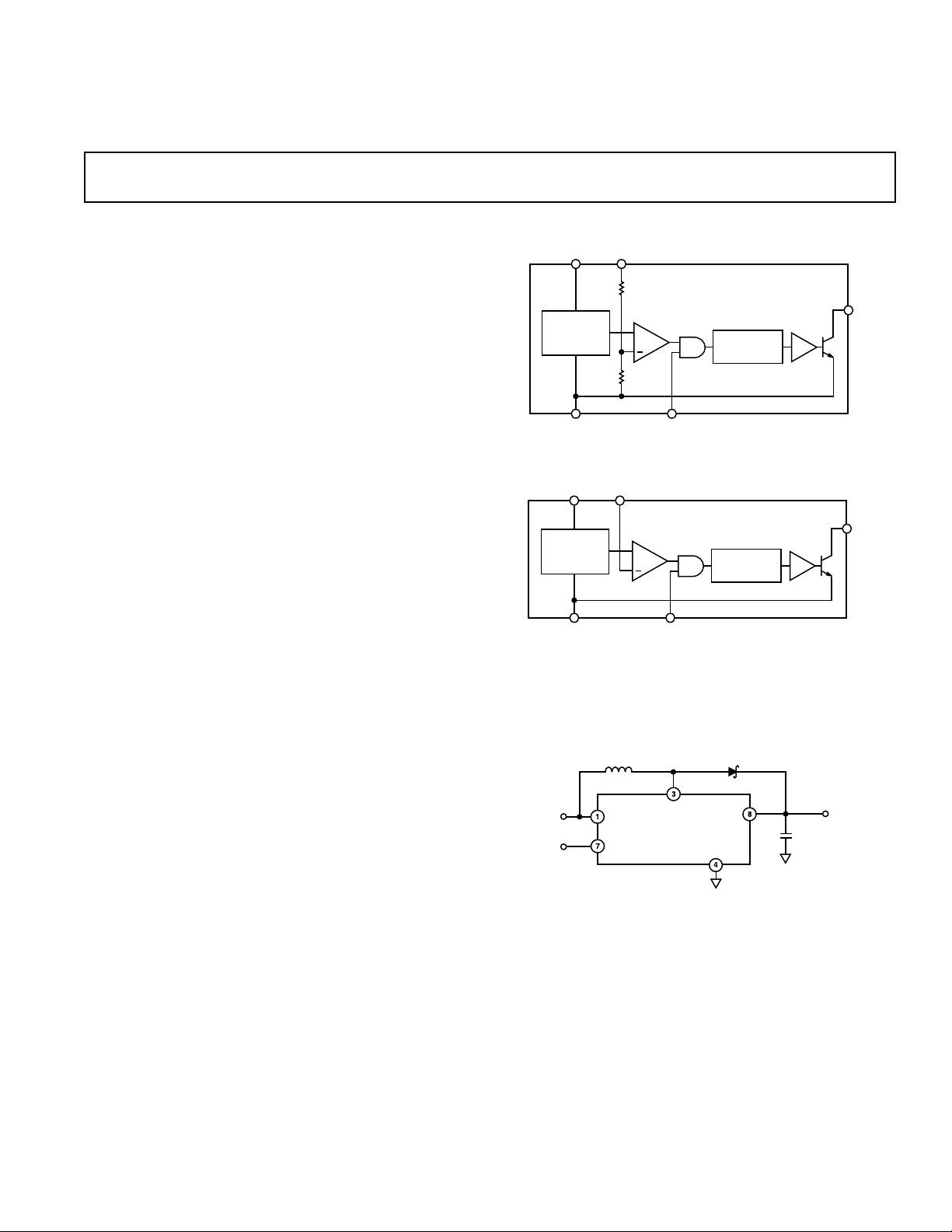
FUNCTIONAL BLOCK DIAGRAMS
Fixed Output
GENERAL DESCRIPTION
The ADP1109 is a versatile step-up switching regulator. The
device requires only minimal external components to operate as
a complete switching regulator.
The ADP1109-5 can deliver 100 mA at 5 V from a 3 V input
and the ADP1109-12 can deliver 60 mA at 12 V from a 5 V
input. The device also features a logic controlled shutdown
capability that, when a logic low is applied, will shut down the
oscillator.
The 120 kHz operating frequency allows for the use of small
surface mount components. The gated oscillator capability
eliminates the need for frequency compensation.
Adjustable Output
TYPICAL APPLICATION
Flash Memory VPP Generator
REV. 0
Information furnished by Analog Devices is believed to be accurate and
reliable. However, no responsibility is assumed by Analog Devices for its
use, nor for any infringements of patents or other rights of third parties
which may result from its use. No license is granted by implication or
otherwise under any patent or patent rights of Analog Devices.
One Technology Way, P.O. Box 9106, Norwood, MA 02062-9106, U.S.A.
Tel: 781/329-4700 World Wide Web Site: http://www.analog.com
Fax: 781/326-8703 © Analog Devices, Inc., 1998

ADP1109–SPECIFICA TIONS
SW
GND
ADP1109-12
+
1N5818
22mF
16V
SENSE
L1
15mH
L1 = CTX15-1
V
IN
= 2V
V
IN
300mA
at 3V INPUT
50mA
at 2V INPUT
+5V
SHUTDOWN
SHUTDOWN
(08C ≤ TA ≤ +708C, VIN = 3 V unless otherwise noted)
Parameter Conditions Symbol Min Typ Max Units
QUIESCENT CURRENT Switch Off I
INPUT VOLTAGE V
Q
IN
29V
450 590 µA
COMPARATOR TRIP POINT
VOLTAGE 1.20 1.25 1.30 V
COMPARATOR HYSTERESIS ADP1109 8 14 mV
OUTPUT VOLTAGE
ADP1109-3.3 2 V ≤ V
ADP1109-5 3 V ≤ V
≤ 3 V V
IN
≤ 5 V 4.75 5.00 5.25 V
IN
OUT
3.13 3.30 3.46 V
ADP1109-12 3 V ≤ VIN ≤ 12 V 11.45 12.00 12.55 V
OUTPUT VOLTAGE RIPPLE ADP1109-3.3 16 40 mV
ADP1109-5 20 50 mV
ADP1109-12 40 110 mV
OSCILLATOR FREQUENCY T
= +25°Cf
A
OSC
100 120 140 kHz
90 155 kHz
DUTY CYCLE Full Load DC 40 50 70 %
SWITCH-ON TIME T
= +25°Ct
A
ON
3.1 4.2 5.9 µs
3.0 6.5 µs
SWITCH SATURATION VOLTAGE I
= 500 mA V
SW
CESAT
ADP1109-3.3 VIN = 3 V 0.4 0.8 V
ADP1109-5 V
= 3 V 0.4 0.8 V
IN
ADP1109-12 VIN = 5 V 0.4 0.8 V
SWITCH LEAKAGE CURRENT VSW = 12 V, TA = +25°C110µA
SHUTDOWN PIN HIGH V
SHUTDOWN PIN LOW V
SHUTDOWN PIN INPUT CURRENT V
SHUTDOWN PIN INPUT CURRENT V
SHUTDOWN
SHUTDOWN
= 2 V I
= 0.8 V I
IH
IL
IH
IL
NOTES
All limits at temperature extremes are guaranteed via correlation using standard quality control methods.
Specifications subject to change without notice.
IN
= 2V
L1 = CTX15-1
L1
15mH
V
IN
ADP1109-12
SW
SENSE
GND
1N5818
+12V
40mA
at 3V INPUT
10mA
at 2V INPUT
10mF
+
20V
L1 = CTX15-1
L1
= 2V
V
IN
15mH
V
ADP1109-5
1N5818
SW
SENSE
IN
GND
+5V
300mA
at 3V INPUT
50mA
at 2V INPUT
22mF
+
16V
V
2.0 V
0.8 V
10 µA
20 µA
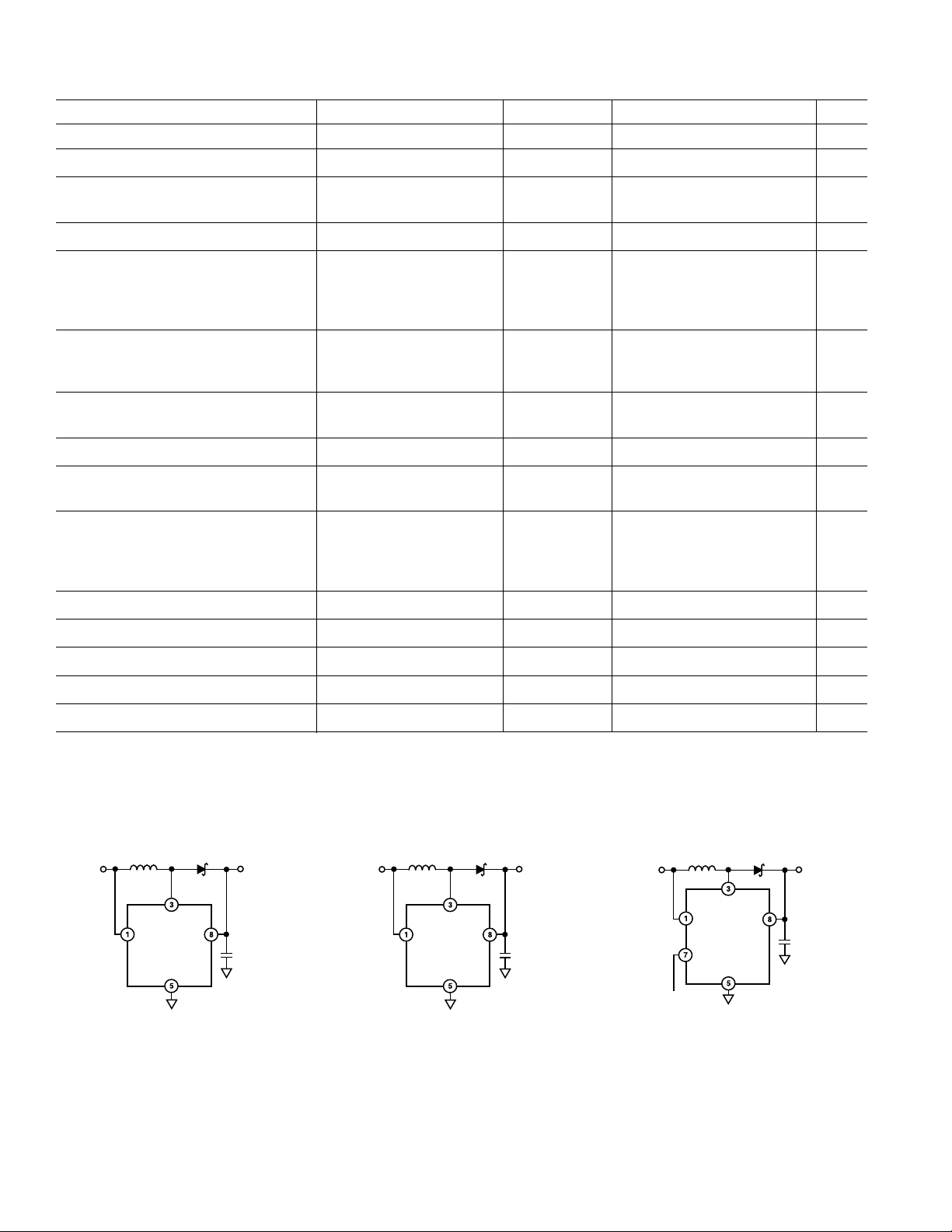
Figure 1. 2 V to 5 V Converter
Figure 2. 2 V to 12 V Converter
–2– REV. 0
Figure 3. 2 V to 5 V Converter
With Shutdown

ADP1109
WARNING!
ESD SENSITIVE DEVICE
ABSOLUTE MAXIMUM RATINGS*
Supply Voltage, V
. . . . . . . . . . . . . . . . . . . . –0.4 V to 20 V
OUT
SW Pin Voltage . . . . . . . . . . . . . . . . . . . . . . . . –0.4 V to 50 V
Shutdown Pin Voltage . . . . . . . . . . . . . . . . . . . . . . . . . . 6.0 V
Switch Current . . . . . . . . . . . . . . . . . . . . . . . . . . . . . . . 1.2 A
Maximum Power Dissipation . . . . . . . . . . . . . . . . . . 300 mW
Operating Temperature Range . . . . . . . . . . . . 0°C to +70°C
Storage Temperature Range . . . . . . . . . . . . –65°C to +150°C
Lead Temperature (Soldering, 10 sec) . . . . . . . . . . . +300°C
*This is a stress rating only; operation beyond these limits can cause the device to
be permanently damaged.
ORDERING GUIDE
Output Package Package
Model Voltage Description Options
ADP1109AN ADJ Plastic DIP N-8
ADP1109AR ADJ Small Outline IC SO-8
ADP1109AN-3.3 3.3 V Plastic DIP N-8
ADP1109AR-3.3 3.3 V Small Outline IC SO-8
ADP1109AN-5 5 V Plastic DIP N-8
ADP1109AR-5 5 V Small Outline IC SO-8
ADP1109AN-12 12 V Plastic DIP N-8
ADP1109AR-12 12 V Small Outline IC SO-8
PIN FUNCTION DESCRIPTIONS
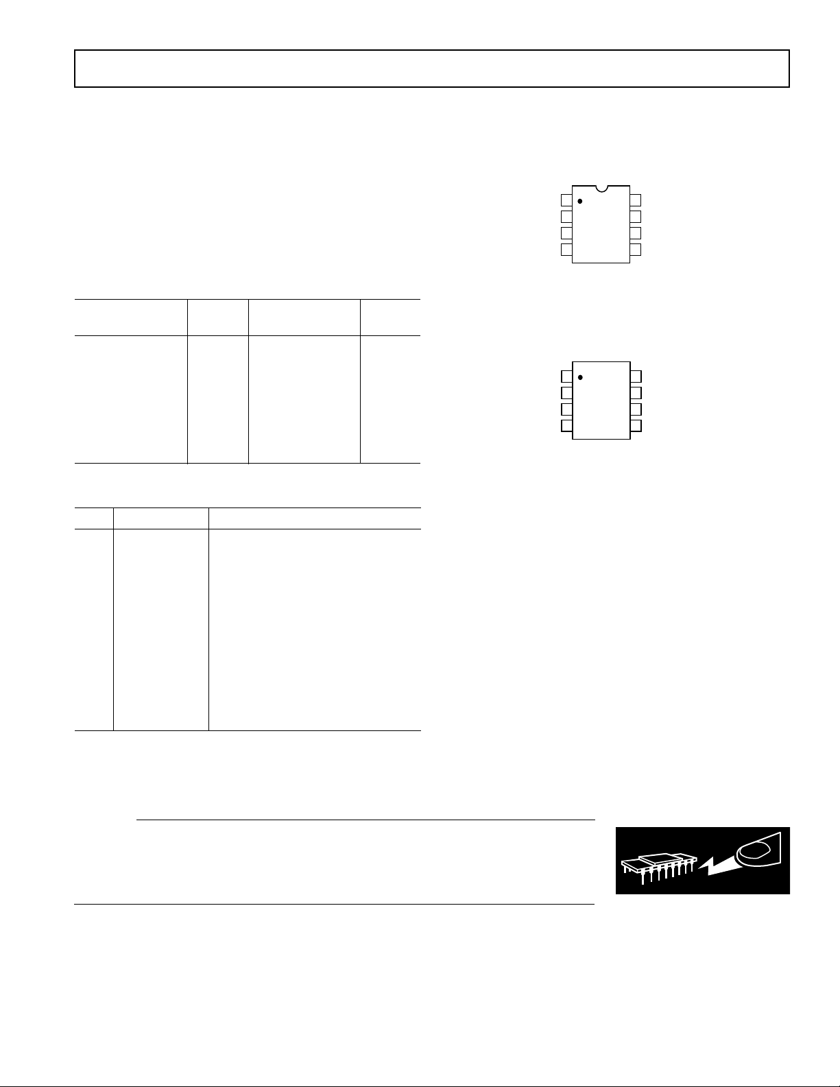
PIN CONFIGURATIONS
8-Lead Plastic DIP
(N-8)
1
V
IN
ADP1109A
2
NC
TOP VIEW
3
SW
(Not to Scale)
4
NC = NO CONNECT
*FIXED VERSIONS
8
FB(SENSE)*
7
SHUTDOWN
6
NC
5
NCGND
8-Lead SOIC
(SO-8)
1
V
IN
ADP1109A
2
NC
TOP VIEW
3
SW
(Not to Scale)
GND
4
NC = NO CONNECT
*FIXED VERSIONS
8
FB(SENSE)*
7
SHUTDOWN
6
NC
5
NC
Pin Mnemonic Function
1V
IN
Input Supply Voltage.
2, 5, 6 NC No Connection.
3 SW Collector Node of Power Transistor.
4 GND Ground.
7 SHUTDOWN When logic low is applied to this pin,
oscillator is shut down.
8 FB(SENSE) On the ADP1109A (Adjustable), this
pin goes directly to the comparator
input. On the ADP1109-3.3,
ADP1109-5 and ADP1109-12, this
pin is connected through the internal
resistor that sets the output voltage.
CAUTION
ESD (electrostatic discharge) sensitive device. Electrostatic charges as high as 4000 V readily
accumulate on the human body and test equipment and can discharge without detection.
Although the ADP1109 features proprietary ESD protection circuitry, permanent damage may
occur on devices subjected to high energy electrostatic discharges. Therefore, proper ESD
precautions are recommended to avoid performance degradation or loss of functionality.
–3–REV. 0
 Loading...