Analog Devices ADP1073 Datasheet

Micropower DC–DC Converter
SET
V
IN
GAIN BLOCK/
ERROR AMP
COMPARATOR
SW2
FBGND
SW1
AO
I
LIM
OSCILLATOR
DRIVER
A1
A2
212mV
REFERENCE
ADP1073
a
Adjustable and Fixed 3.3 V, 5 V, 12 V
FEATURES
Operates at Supply Voltages from 1.0 V to 30 V
Ground Current 100 mA
Works in Step-Up or Step-Down Mode
Very Few External Components Required
Low Battery Detector On-Chip
User-Adjustable Current Limit
Internal 1 A Power Switch
Fixed and Adjustable Output Voltage Versions
8-Lead DIP or SO-8 Package
APPLICATIONS
Single-Cell to 5 V Converters
Laptop and Palmtop Computers
Pagers
Cameras
Battery Backup Supplies
Cellular Telephones
Portable Instruments
4 mA–20 mA Loop Powered Instruments
Hand-Held Inventory Computers
GENERAL DESCRIPTION
The ADP1073 is part of a family of step-up/step-down switching regulators that operates from an input supply voltage of as
little as 1.0 V. This extremely low input voltage allows the
ADP1073 to be used in applications requiring use of a single
cell battery as the primary power source.
The ADP1073 can be configured to operate in either step-up or
step-down mode but for input voltages greater than 3 V, the
ADP1173 is recommended.
An auxiliary gain amplifier can serve as a low battery detector or
linear regulator. Quiescent current on the ADP1073-5 is only
100 µA unloaded, making it ideal for systems where long battery
life is required.
The ADP1073 can deliver 40 mA at 5 V from an input voltage
range as low as 1.25 V, or 10 mA at 5 V from a 1.0 V input.
Current limiting is available by adding an external resistor.
V
IN
ADP1073
FUNCTIONAL BLOCK DIAGRAMS
ADP1073
SET
ADP1073-3.3
ADP1073-5
ADP1073-12
OSCILLATOR
ADP1073-3.3: R1 = 62.1kV
ADP1073-5: R1 = 40kV
ADP1073-12: R1 = 16.3kV
212mV
REFERENCE
A2
GAIN BLOCK/
ERROR AMP
A1
R1
COMPARATOR
R2
904kV
ADP1073-3.3, 5, 12
SENSEGND
DRIVER
AO
I
LIM
SW1
SW2
REV. 0
Information furnished by Analog Devices is believed to be accurate and
reliable. However, no responsibility is assumed by Analog Devices for its
use, nor for any infringements of patents or other rights of third parties
which may result from its use. No license is granted by implication or
otherwise under any patent or patent rights of Analog Devices.
One Technology Way, P.O. Box 9106, Norwood, MA 02062-9106, U.S.A.
Tel: 781/329-4700 World Wide Web Site: http://www.analog.com
Fax: 781/326-8703 © Analog Devices, Inc., 1997

ADP1073–SPECIFICATIONS
(@ TA = 08C to +708C, VIN = 1.5 V unless otherwise noted)
Parameter Conditions Symbol Min Typ Max Units
QUIESCENT CURRENT Switch Off I
QUIESCENT CURRENT, STEP-UP No Load, ADP1073-3.3 I
Q
Q
100 165 µA
100 µA
MODE CONFIGURATION ADP1073-5 100 µA
ADP1073-12, T
INPUT VOLTAGE Step-Up Mode V
Step-Up Mode, T
= +25°C 100 µA
A
= +25°C 1.0 12.6 V
A
IN
1.15 12.6 V
Step-Down Mode 30 V
COMPARATOR TRIP POINT VOLTAGE ADP1073
OUTPUT SENSE VOLTAGE ADP1073-3.3
ADP1073-5
ADP1073-12
1
2
2
2
V
OUT
200 212 222 mV
3.14 3.30 3.47 V
4.75 5.00 5.25 V
11.4 12.00 12.6 V
COMPARATOR HYSTERESIS ADP1073 5 10 mV
OUTPUT HYSTERESIS ADP1073-3.3 90 130 mV
ADP1073-5 125 250 mV
ADP1073-12 300 600 mV
OSCILLATOR FREQUENCY f
MAXIMUM DUTY CYCLE Full Load (V
FB
< V
) DC 577280 %
REF
SWITCH ON TIME t
FEEDBACK PIN BIAS CURRENT ADP1073 VFB = 0 V I
SET PIN BIAS CURRENT V
AO OUTPUT LOW I
REFERENCE LINE REGULATION 1.0 V ≤ V
SWITCH SATURATION VOLTAGE V
STEP-UP MODE T
A2 ERROR AMP GAIN R
REVERSE BATTERY CURRENT
4
CURRENT LIMIT 220 Ω Between I
= V
SET
REF
= 100 µAV
AO
≤ 1.5 V 0.35 %/V
1.5 V ≤ V
IN
MIN
V
IN
T
MIN
V
IN
T
MIN
L
T
A
T
A
IN
≤ 12 V 0.05 0.15 %/V
IN
= 1.5 V, I
to T
= 1.5 V, I
to T
= 5 V, I
to T
= 100 kΩ
= 400 mA, +25°CV
SW
MAX
= 500 mA, +25°C 400 550 mV
SW
MAX
= 1 A, +25°C 700 1000 mV
SW
MAX
3
= +25°CI
and V
LIM
IN
= +25°CI
OSC
ON
FB
I
SET
AO
CESAT
A
V
REV
LIM
14 19 24 kHz
28 38 50 µs
60 300 nA
100 220 nA
0.15 0.4 V
300 450 mV
600 mV
750 mV
1500 mV
400 1000 V/V
750 mA
400 mA
CURRENT LIMIT TEMPERATURE
COEFFICIENT –0.3 %/°C
SWITCH-OFF LEAKAGE CURRENT Measured at SW1 Pin
T
= +25°CI
A
MAXIMUM EXCURSION BELOW GND I
NOTES
1
This specification guarantees that both the high and low trip point of the comparator fall within the 200 mV to 222 mV range.
2
This specification guarantees that the output voltage of the fixed versions will always fall within the specified range. The waveform at the sense pin will exhibit a
sawtooth shape due to the comparator hysteresis.
3
100 kΩ resistor connected between a 5 V source and the AO pin.
4
The ADP1073 is guaranteed to withstand continuous application of +1.6 V applied to the GND and SW2 pins while VIN, I
All limits at temperature extremes are guaranteed via correlation using standard Quality Control methods.
Specifications subject to change without notice.
≤ 10 µA, Switch Off
SW1
T
= +25°CV
A
LEAK
SW2
LIM
–2–
115µA
–400 –350 mV
and SW1 pins are grounded.
REV. 0

ADP1073
1
2
3
4
8
7
6
5
TOP VIEW
(Not to Scale)
ADP1073
I
LIM
V
IN
SW1
SW2
FB (SENSE)*
SET
AO
GND
* FIXED VERSIONS
1
2
3
4
8
7
6
5
TOP VIEW
(Not to Scale)
ADP1073
I
LIM
V
IN
SW1
SW2
FB (SENSE)*
SET
AO
GND
* FIXED VERSIONS
ABSOLUTE MAXIMUM RATINGS
Input Supply Voltage, Step-Up Mode . . . . . . . . . . . . . . . 15 V
Input Supply Voltage, Step-Down Mode . . . . . . . . . . . . . 36 V
SW1 Pin Voltage . . . . . . . . . . . . . . . . . . . . . . . . . . . . . . . 50 V
SW2 Pin Voltage . . . . . . . . . . . . . . . . . . . . . . . . .–0.4 V to V
IN
Feedback Pin Voltage (ADP1073) . . . . . . . . . . . . . . . . . . . 5 V
Switch Current . . . . . . . . . . . . . . . . . . . . . . . . . . . . . . . .1.5 A
Maximum Power Dissipation . . . . . . . . . . . . . . . . . . 500 mW
Operating Temperature Range (A) . . . . . . . . . . 0°C to +70°C
Storage Temperature Range . . . . . . . . . . . . –65°C to +150°C
Lead Temperature (Soldering, 10 sec) . . . . . . . . . . . .+300°C
CADDELL-BURNS
7200-12
82mH
I
V
LIM
IN
1.5V
AA CELL*
OPERATES WITH CELL VOLTAGE
*ADD 10mF DECOUPLING CAPACITOR IF BATTERY
IS MORE THAN 2 INCHES AWAY FROM ADP1073
ADP1073-5
GND
SW1
SENSE
SW2
1N5818
$1.0V
+5V
40mA
100mF
SANYO
OS-CON
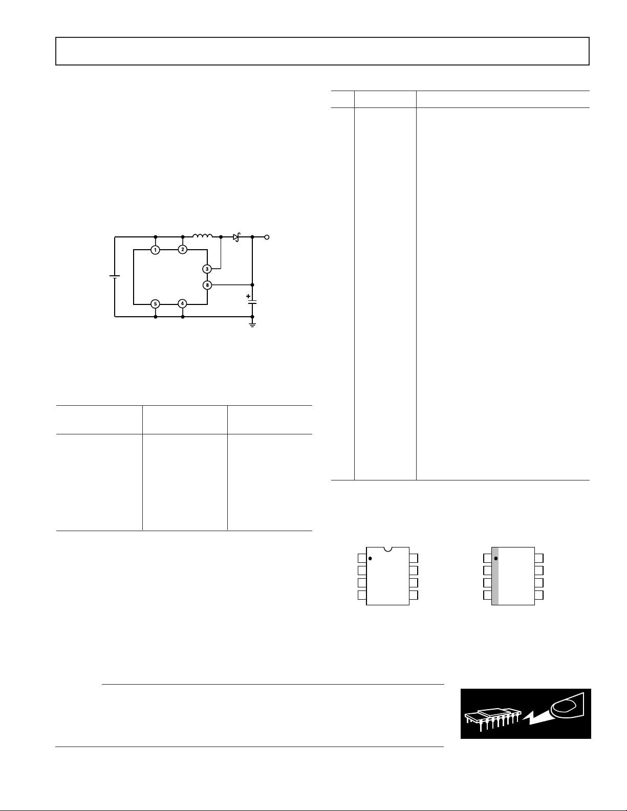
Figure 1. Typical Application
ORDERING GUIDE
Output Package
Model* Voltage Options**
ADP1073AN ADJ N-8
ADP1073AR ADJ SO-8
ADP1073AN-3.3 3.3 V N-8
ADP1073AR-3.3 3.3 V SO-8
ADP1073AN-5 5 V N-8
ADP1073AR-5 5 V SO-8
ADP1073AN-12 12 V N-8
ADP1073AR-12 12 V SO-8
NOTES
**Temperature Range: 0°C to +70°C.
**N = Plastic DIP; SO = Small Outline Package.
PIN FUNCTION DESCRIPTIONS
Pin Mnemonic Function
1I
LIM
For normal conditions this pin is connected to V
. When a lower current
IN
limit is required, a resistor should be
connected between I
LIM
and V
IN.
Limit-
ing the switch current to 400 mA is
achieved by connecting a 220 Ω resistor.
2V
IN
Input Voltage.
3 SW1 Collector Node of Power Transistor.
For step-down configuration, connect to
for step-up configuration, connect
V
IN;
to an inductor/diode.
4 SW2 Emitter Node of Power Transistor. For
step- down configuration, connect to
inductor/diode; for step-up configuration, connect to ground. Do not allow
this pin to drop more than a diode drop
below ground.
5 GND Ground.
6 AO Auxiliary Gain (GB) Output. The open
collector can sink 100 µA.
7 SET Gain Amplifier Input. The amplifier’s
positive input is connected to the SET
pin and its negative input is connected
to the 212 mV reference.
8 FB/SENSE On the ADP1073 (adjustable) version
this pin is connected to the comparator
input. On the ADP1073-3.3, ADP1073-
5 and ADP1073-12, the pin goes di-
rectly to the internal application resistor
that sets output voltage.
PIN CONFIGURATIONS
8-Lead Plastic DIP 8-Lead Small Outline Package
(N-8) (SO-8)
CAUTION
ESD (electrostatic discharge) sensitive device. Electrostatic charges as high as 4000 V readily
accumulate on the human body and test equipment and can discharge without detection.
Although the ADP1073 features proprietary ESD protection circuitry, permanent damage may
occur on devices subjected to high energy electrostatic discharges. Therefore, proper ESD
precautions are recommended to avoid performance degradation or loss of functionality.
REV. 0
–3–
WARNING!
ESD SENSITIVE DEVICE

ADP1073
TEMPERATURE – 8C
34.5
30
240
085
25 70
32
31.5
31
30.5
34
33.5
33
32.5
SWITCH-ON TIME – ms
–Typical Performance Characteristics
1.2
1
0.8
Volts
0.6
(SAT) –
CE
0.4
V
0.2
VIN = 5.0V
V
= 3.0V
IN
VIN = 1.0V
0
0.1 0.2 1.20.3 0.4 0.5 0.6 0.7 0.8 0.9 1 1.1
SWITCH CURRENT – Amps
V
IN
= 1.25V
VIN = 1.5V
V
IN
= 2.0V
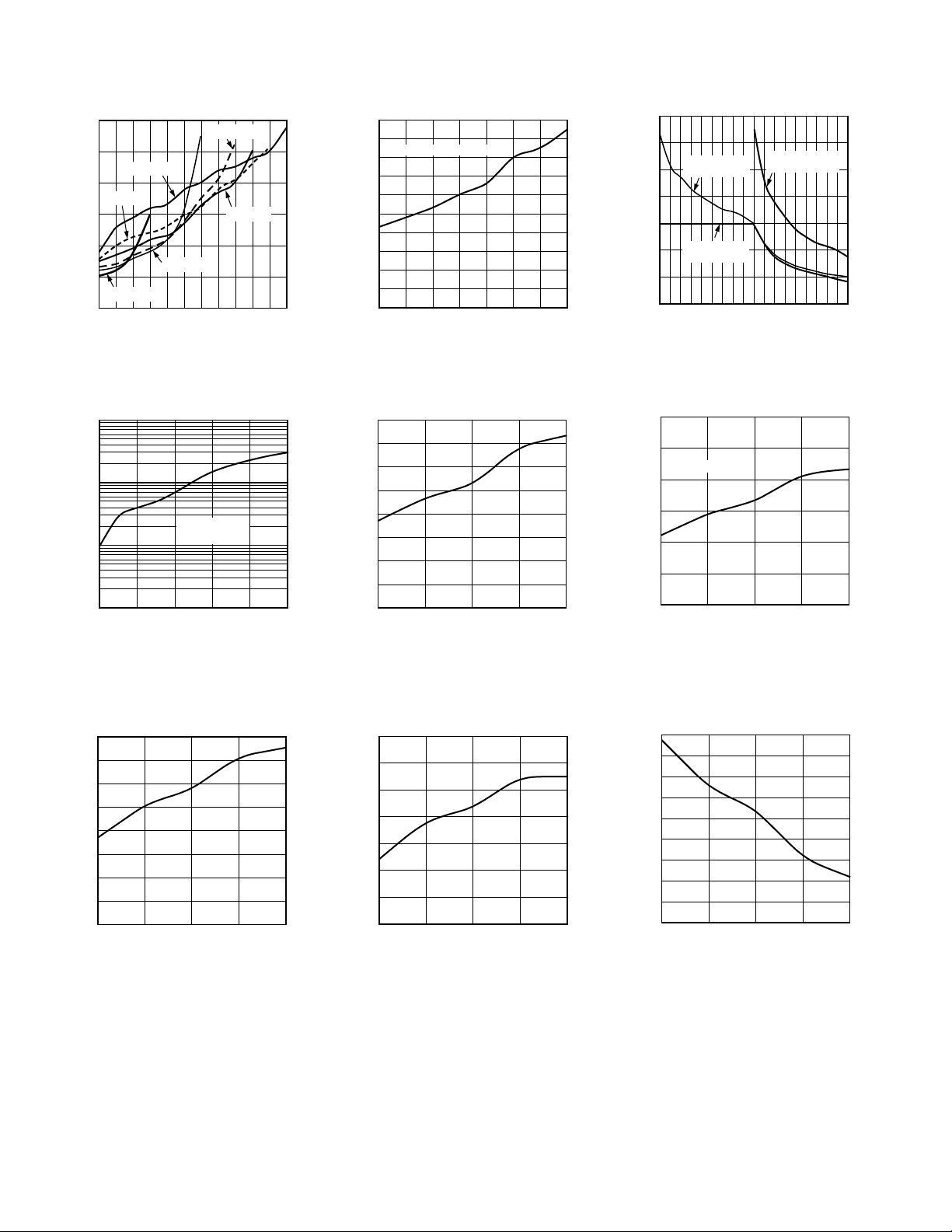
Figure 2. Saturation Voltage vs.
Switch Current in Step-Up Mode
1000
100
FOR VIN > 1.6V,
R
= 68V
10
OUTPUT CURRENT – mA
0
1 3.5
1.5 2 2.5 3
INPUT VOLTAGE – Volts
LIM
Figure 5. Guaranteed Minimum
Output Current at V
= 5 V vs.
OUT
Input Voltage
2
1.8
SATURATION VOLTAGE
1.6
1.4
1.2
1
0.8
0.6
0.4
SWITCH ON VOLTAGE – Volts
0.2
0
0.05
0.2 0.3 0.4 0.5 0.6
0.1 0.7
SWITCH CURRENT – Amps
Figure 3. Switch ON Voltage vs.
Switch Current in Step-Down Mode
120
110
100
90
80
70
60
SET PIN BIAS CURRENT – nA
50
40
240
085
25 70
TEMPERATURE – 8C
Figure 6. Set Pin Bias Current vs.
Temperature
1400
1200
800
600
400
200
0
10 100030
VIN = 3V
WITH L = 82mH
VIN = 1.5V
WITH L = 82mH
50
70 90 200 400 600 800
1000
SWITCH CURRENT – mA
VIN = 12V
WITH L = 150mH
R
– V
LIM
Figure 4. Maximum Switch Current
vs. R
LIM
160
140
120
100
SUPPLY CURRENT – mA
VIN = 1.5V
80
60
40
240
085
25 70
TEMPERATURE – 8C
Figure 7. Supply Current vs.
Temperature
22
21
20
19
18
17
16
15
OSCILLATOR FREQUENCY – kHz
14
240
08525 70
TEMPERATURE – 8C
Figure 8. Oscillator Frequency vs.
Temperature
70
68
66
64
62
60
DUTY CYCLE – %
58
56
240
085
25 70
TEMPERATURE – 8C
Figure 9. Duty Cycle vs. Temperature
–4–
Figure 10. Switch ON Time vs.
Temperature
REV. 0

2300
ADP1073
2100
1900
1700
1500
GAIN BLOCK GAIN – V/V
1300
1100
240
085
TEMPERATURE – 8C
Figure 11. “Gain Block” Gain vs. Temperature
THEORY OF OPERATION
The ADP1073 is a flexible, low power switch mode power
supply (SMPS) controller. The regulated output voltage can be
greater than the input voltage (boost or step-up mode) or less
than the input (buck or step-down mode). This device uses a
gated-oscillator technique to provide very high performance
with low quiescent current.
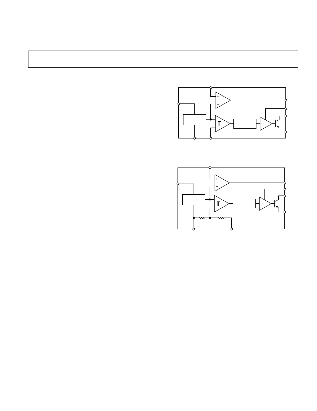
A functional block diagram of the ADP1073 is shown on the
front page. The internal 212 mV reference is connected to one
input of the comparator, while the other input is externally
connected (via the FB pin) to a feedback network connected to
the regulated output. When the voltage at the FB pin falls below
212 mV, the 19 kHz oscillator turns on. A driver amplifier provides base drive to the internal power switch and the switching
action raises the output voltage. When the voltage at the FB pin
exceeds 212 mV, the oscillator is shut off. While the oscillator is
off, the ADP1073 quiescent current is only 100 µA. The com-
parator includes a small amount of hysteresis, which ensures
loop stability without requiring external components for frequency compensation.
The maximum current in the internal power switch can be set
by connecting a resistor between V
IN
and the I
pin. When
LIM
the maximum current is exceeded, the switch is turned OFF.
The current limit circuitry has a time delay of about 2 µs. If an
external resistor is not used, connect I
mation on I
is included in the Limiting the Switch Current
LIM
to VIN. Further infor-
LIM
section of this data sheet.
The ADP1073 internal oscillator provides 38 µs ON and 15 µs
OFF times, which is ideal for applications where the ratio between V
and V
IN
is roughly a factor of three (such as gener-
OUT
ating +5 V from a single 1.5 V cell). Wider range conversions,
as well as step-down converters, can also be accomplished with
a slight loss in the maximum output power that can be obtained.
VIN = 1.5V
= 100kV
R
L
25 70
An uncommitted gain block on the ADP1073 can be connected
as a low-battery detector, linear post-regulator or undervoltage
lockout detector. The inverting input of the gain block is internally connected to the 212 mV reference. The noninverting
input is available at the SET pin. A resistor divider, connected
between V
and GND with the junction connected to the SET
IN
pin, causes the AO output to go LOW when the input voltage
goes below the low battery set point. The AO output is an open
collector NPN transistor that can sink 100 µA.
The ADP1073 provides external connections for both the collector and emitter of its internal power switch, which permits
both step-up and step-down modes of operation. For the stepup mode, the emitter (Pin SW2) is connected to GND and the
collector (Pin SW1) drives the inductor. For step-down mode,
the emitter drives the inductor while the collector is connected
.
to V
IN
The output voltage of the ADP1073 is set with two external
resistors. Three fixed-voltage models are also available:
ADP1073-3.3 (+3.3 V), ADP1073-5 (+5 V) and ADP1073-12
(+12 V). The fixed-voltage models are identical to the ADP1073,
except that laser-trimmed voltage-setting resistors are included
on the chip. Only three external components are required to
form a +3.3 V, +5 V or +12 V converter. On the fixed-voltage
models of the ADP1073, simply connect the feedback pin (Pin
8) directly to the output voltage.
The ADP1073 oscillator only turns on when the output voltage
is below the programmed voltage. When the output voltage is
above the programmed voltage, the ADP1073 remains in its
quiescent state to conserve power. Output ripple, which is inherent in gated oscillator converters, is typically 125 mV for a
5 V output and 300 mV for a 12 V output. This ripple voltage
can be greatly reduced by inserting the gain-block between the
output and the FB pin. Further information and a typical circuit
are shown in the Programming the Gain Block section.
REV. 0
–5–
 Loading...