Digital Power Factor Correction Controller
R
Data Sheet
FEATURES
Flexible digital power factor correction (PFC) controller
Single phase operation (ADP1047); interleaved and
bridgeless operation (ADP1048)
True rms ac power metering
Enhanced dynamic response
Optimized light load efficiency performance
Output voltage adjustment
Frequency reduction
Inrush current control
Switching frequency spread spectrum for improved EMI
External frequency synchronization
PMBus compliant
Programmable ac line fault detection and protection
Programmable output fault detection and protection
Extensive fault protection for high reliability systems
Frequency range from 30 kHz to 400 kHz
8 kB EEPROM
Programming via easy-to-use graphical user interface (GUI)
APPLICATIONS
AC/DC power supplies for applications
Computing server and storage
Network and communication infrastructure
Industrial and medical
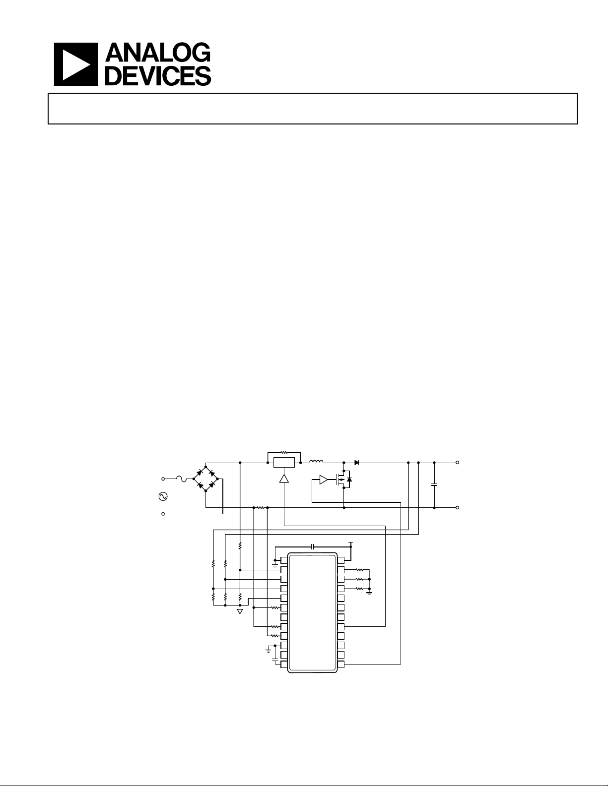
TYPICAL APPLICATIONS CIRCUIT
V
REC
RELAY
with Accurate AC Power Metering
ADP1047/ADP1048
GENERAL DESCRIPTION
The ADP1047/ADP1048 are digital power factor correction
(PFC) controllers that provide accurate input power metering
capability and inrush current control for ac/dc systems. The
ADP1047 is designed for single phase PFC applications; the
ADP1048 is designed especially for interleaved and bridgeless
PFC applications.
The digital PFC function is based on a conventional boost PFC
with multiplication of the output voltage feedback combined with
the input current and voltage to provide optimum harmonic
correction and power factor for ac/dc systems. All signals are
converted into the digital domain to provide maximum flexibility;
all key parameters can be reported and adjusted via the PMBus™
interface. The ADP1047/ADP1048 allow users to optimize system
performance, maximize efficiency across the load range, and
reduce design time to market.
The ADP1047/ADP1048 provide accurate rms measurement
of input voltage, current, and power. This information can be
reported to the microcontroller of the power supply via the
PMBus interface.
V
OUT
AC
INPUT
1
AGND
2
VAC
3
VFB
4
OVP
5
PGND
6
ILIM
7
NC
8
CS–
9
CS+
10
DGND
11
PSON
12
VCORE
Rev. 0
Information furnished by Analog Devices is believed to be accurate and reliable. However, no
responsibility is assumed by Analog Devices for its use, nor for any infringements of patents or other
rights of third parties that may result from its use. Specifications subject to change without notice. No
license is granted by implication or otherwise under any patent or patent rights of Analog Devices.
Trademarks and registered trademarks are the property of their respective owners.
BULK
CAPACITO
3.3V
24
VDD
23
RES
22
RTD
21
ADD
20
SDA
PMBus
19
SCL
18
SYNC
17
INRUSH
16
PGOOD
15
AC_OK
14
PWM2
13
PWM
ADP1047
09696-101
Figure 1.
One Technology Way, P.O. Box 9106, Norwood, MA 02062-9106, U.S.A.
Tel: 781.329.4700 www.analog.com
Fax: 781.461.3113 ©2011 Analog Devices, Inc. All rights reserved.

ADP1047/ADP1048 Data Sheet
TABLE OF CONTENTS
Features .............................................................................................. 1
Applications ....................................................................................... 1
General Description ......................................................................... 1
Typical Applications Circuit ............................................................ 1
Revision History ............................................................................... 4
Specifications ..................................................................................... 6
Absolute Maximum Ratings ............................................................ 9
Thermal Resistance ...................................................................... 9
ESD Caution .................................................................................. 9
Pin Configurations and Function Descriptions ......................... 10
Functional Block Diagrams ........................................................... 11
Controller Architecture ................................................................. 12
Current Sense .............................................................................. 12
RMS Input Overcurrent Protection ......................................... 12
Fast Overcurrent Protection (ILIM Pin) ................................. 12
Current Balancing (IBAL Pin, ADP1048 Only) ..................... 14
Voltage Sense ............................................................................... 14
Overvoltage Protection .............................................................. 15
Power Factor Correction Control Loop ...................................... 17
Digital Compensation Filters .................................................... 17
Pulse-Width Modulation ........................................................... 18
Duty Cycle Minimum/Maximum Limits ................................ 18
Auxiliary PWM Output (ADP1047 Only) .............................. 18
Switching Frequency Programming ........................................ 19
Line Fault Protections and Soft Start Sequencing ...................... 20
PSON Operation ........................................................................ 20
AC Line Detection ...................................................................... 20
Soft Start Procedure ................................................................... 22
Line Fault Protections ................................................................ 22
Advanced Input Power Metering.................................................. 24
Power Supply System and Fault Monitoring ............................... 25
Flag Conventions ........................................................................ 25
Manufacturer-Specific Flags ..................................................... 25
Standard PMBus Flags ............................................................... 26
PMBus Fault Flag Response ...................................................... 27
Manufacturer-Specific Flag Response ..................................... 28
Monitoring Functions ................................................................ 29
First Error Fault .......................................................................... 29
Overtemperature Protection (OTP) ........................................ 29
AC_OK and PGOOD Signals ................................................... 29
Advanced Features ......................................................................... 30
Frequency Dithering (Spread Spectrum) ................................ 30
PWM Frequency Synchronization ........................................... 30
Smart Output Voltage (Load Line) .......................................... 30
Smart Switching Frequency ...................................................... 31
Current Loop Filter for Light Load .......................................... 31
Phase Shedding (ADP1048 Only) ............................................ 31
Current Loop Feedforward ....................................................... 31
Bridgeless Boost Operation (ADP1048 Only)........................ 32
Power Supply System Calibration and Trim ............................... 33
Output Voltage (VFB) Calibration and Trim ......................... 33
Input Voltage (VAC) Gain and Offset Trim ............................ 33
Current Sense Gain and Offset Trim ....................................... 33
Input Power Gain and Offset Trim .......................................... 33
PMBus Digital Communication ................................................... 34
Features ........................................................................................ 34
Overview ..................................................................................... 34
PMBus Address .......................................................................... 34
Data Transfer............................................................................... 35
General Call Support ................................................................. 36
Fast Mode .................................................................................... 36
Fault Conditions ......................................................................... 36
Timeout Condition .................................................................... 36
Data Transmission Faults .......................................................... 37
Data Content Faults ................................................................... 37
EEPROM ......................................................................................... 38
Overview ..................................................................................... 38
Page Erase Operation ................................................................. 38
Read Operation (Byte Read and Block Read) ........................ 38
Write Operation (Byte Write and Block Write) ..................... 39
EEPROM Password .................................................................... 39
Downloading EEPROM Settings to Internal Registers ......... 39
Saving Register Settings into EEPROM .................................. 40
EEPROM CRC Checksum ........................................................ 40
Software GUI .................................................................................. 41
Standard PMBus Commands Supported by the
ADP1047/ADP1048 ....................................................................... 42
Manufacturer-Specific PMBus Commands ................................ 43
Detailed Register Descriptions ..................................................... 45
OPERATION Register ............................................................... 45
Rev. 0 | Page 2 of 84

Data Sheet ADP1047/ADP1048
ON_OFF_CONFIG Register ..................................................... 45
CLEAR_FAULTS Command ..................................................... 45
WRITE_PROTECT Register ..................................................... 45
RESTORE_DEFAULT_ALL Command .................................. 45
STORE_USER_ALL Command ................................................ 45
RESTORE_USER_ALL Command .......................................... 46
CAPABILITY Register ............................................................... 46
VOUT_MODE Register ............................................................. 46
VOUT_COMMAND Register .................................................. 46
VOUT_SCALE_LOOP Register ............................................... 46
VOUT_SCALE_MONITOR Register ...................................... 47
VIN_ON Register........................................................................ 47
VIN_OFF Register ...................................................................... 47
VOUT_OV_FAULT_LIMIT Register ...................................... 47
VOUT_OV_FAULT_RESPONSE Register ............................. 47
VOUT_OV_WARN_LIMIT Register ...................................... 48
VOUT_UV_WARN_LIMIT Register ...................................... 48
VOUT_UV_FAULT_LIMIT Register ...................................... 48
VOUT_UV_FAULT_RESPONSE Register ............................. 49
OT_FAULT_RESPONSE Register ............................................ 49
VIN_OV_FAULT_LIMIT Register........................................... 50
VIN_OV_FAULT_RESPONSE Register .................................. 50
VIN_UV_WARN_LIMIT Register ........................................... 51
VIN_UV_FAULT_LIMIT Register .......................................... 51
VIN_UV_FAULT_RESPONSE Register .................................. 52
IIN_OC_FAULT_LIMIT Register ............................................ 52
IIN_OC_FAULT_RESPONSE Register ................................... 53
IIN_OC_WARN_LIMIT Register ............................................ 53
PIN_OP_WARN_LIMIT Register ............................................ 54
STATUS_BYTE Register ............................................................ 54
STATUS_WORD Register ......................................................... 54
STATUS_VOUT Register ........................................................... 55
STATUS_INPUT Register ......................................................... 55
STATUS_TEMPERATURE Register ........................................ 55
READ_VIN Register ................................................................... 55
READ_IIN Register .................................................................... 55
READ_VOUT Register .............................................................. 56
READ_PIN Register ................................................................... 56
PMBUS_REVISION Register .................................................... 56
MFR_ID Register ........................................................................ 56
MFR_MODEL Register .............................................................. 56
MFR_REVISION Register ......................................................... 56
EEPROM_DATA_00 Through EEPROM_DATA_15
Commands ................................................................................... 56
EEPROM_CRC_CHKSUM Register ....................................... 57
EEPROM_NUM_RD_BYTES Register ................................... 57
EEPROM_ADDR_OFFSET Register ....................................... 57
EEPROM_PAGE_ERASE Register ........................................... 57
EEPROM_PASSWORD Register .............................................. 57
TRIM_PASSWORD Register .................................................... 57
EEPROM_INFO Command ..................................................... 57
CS_FAST_OCP_RESPONSE Register ..................................... 58
OVP_FAST_OVP_RESPONSE Register ................................. 58
OLP_RESPONSE Register ......................................................... 58
VDD3P3_RESPONSE Register ................................................. 59
VCORE_RESPONSE Register ................................................... 59
PGOOD_AC_OK_DEBOUNCE_SET Register ..................... 59
PSON_SET Register ................................................................... 60
FLAG_FAULT_ID Register ....................................................... 60
SOFTSTART_FLAGS_BLANK1 Register ............................... 61
SOFTSTART_FLAGS_BLANK2 Register ............................... 61
PGOOD_FLAGS_LIST Register ............................................... 61
AC_OK_FLAGS_LIST Register ................................................ 61
PWM and PWM2 Timing Registers ........................................ 62
PWM_SET Register .................................................................... 63
PWM_LIMIT Register ............................................................... 63
RTD ADC Offset Trim Setting (MSB) Register ...................... 63
RTD ADC Offset Trim Setting (LSB) Register ....................... 63
RTD ADC Gain Trim Setting Register .................................... 64
OT_FAULT_LIMIT Register ..................................................... 64
OT_WARN_LIMIT Register ..................................................... 64
Switching Frequency Setting Register ...................................... 65
Low Power Switching Frequency Setting Register ................. 66
Frequency Dithering Set Register ............................................. 67
Frequency Synchronization Set Register ................................. 68
Voltage Loop Filter Gain Register ............................................. 68
Voltage Loop Filter Zero Register ............................................. 68
Fast Voltage Loop Filter Gain Register ..................................... 68
Fast Voltage Loop Filter Zero Register ..................................... 68
Fast Voltage Loop Enable Register ............................................ 68
VAC_THRESHOLD_SET Register .......................................... 69
VAC_THRESHOLD_READ Register ...................................... 69
Rev. 0 | Page 3 of 84

ADP1047/ADP1048 Data Sheet
MIN_AC_PERIOD_SET Register ........................................... 69
MAX_AC_PERIOD_SET Register .......................................... 69
Current Loop Filter Gain for Low Line Input Register ......... 70
Current Loop Filter Zero for Low Line Input Register ......... 70
Current Loop Filter Gain for High Line Input Register ........ 70
Current Loop Filter Zero for High Line Input Register ........ 70
Soft Start Set Register ................................................................. 70
Inrush Set Register ..................................................................... 71
FAST_OVP_FAULT_RISE Register ......................................... 71
FAST_OVP_FAULT_FALL Register ........................................ 71
FAST OVP Debounce Time Setting Register ......................... 71
Low Power Mode Operation Threshold Register .................. 72
Power Metering Offset Trim for Low Line Input Register .... 72
Power Metering Gain Trim for Low Line Input Register ...... 72
High Line Limit Register ........................................................... 72
Low Line Limit Register ............................................................ 72
ILIM_TRIM Register ................................................................. 72
Voltage Loop Output Register .................................................. 72
Exponent Register ...................................................................... 73
Read Update Rate Register ........................................................ 73
VIN Scale Monitor Register ...................................................... 73
IIN_GSENSE Register ............................................................... 73
CS Fast OCP Blank Register ..................................................... 74
CS Fast OCP Setting Register ................................................... 74
Temperature Hysteresis Register .............................................. 74
VAC ADC Gain Trim Register ................................................. 75
VFB ADC Gain Trim Register .................................................. 75
CS ADC Gain Trim for 500 mV Range Register .................... 75
IBAL Gain Register (ADP1048 Only) ..................................... 75
Smart VOUT Low Power Threshold (P1) Register ............... 75
Smart VOUT High Power Threshold (P2) Register .............. 75
Smart VOUT Low Line (VOL1) Register ................................ 76
Smart VOUT Low Line (VOL2) Register ................................ 76
Smart VOUT High Line (VOH1) Register ............................. 76
Smart VOUT High Line (VOH2) Register ............................. 76
Smart VOUT Upper Limit (VOH) Register ........................... 76
Smart VOUT Super High Line Register .................................. 76
SYNC Delay Register ................................................................. 76
SMART_VOUT_SUPER_HIGH_LINE_HYS Register ........ 77
POWER_HYS Register .............................................................. 77
Advanced Feature Enable Register ........................................... 77
VOUT_OV_FAULT_HYS Register ......................................... 77
VIN_UV_FAULT_HYS Register .............................................. 77
VAC ADC Offset Trim Register ............................................... 78
CS ADC Offset Trim for 500 mV Range Register ................. 78
CS ADC Gain Trim for High (750 mV) Range Register....... 78
CS ADC Offset Trim for High (750 mV) Range Register .... 78
Latched Flag Registers ............................................................... 78
PWM Value Register .................................................................. 79
VAC_LINE_PERIOD Register ................................................. 79
Read Temperature ADC Register ............................................. 79
Power Metering Offset Trim for High Line Input Register .. 79
Power Metering Gain Trim for High Line Input Register .... 80
Current Loop Filter Gain for Low Line Input and Light
Load Register .............................................................................. 80
Current Loop Filter Zero for Low Line Input and Light
Load Register .............................................................................. 80
Current Loop Filter Gain for High Line Input and Light
Load Register .............................................................................. 80
Current Loop Filter Zero for High Line Input and Light
Load Register .............................................................................. 80
Smart VOUT Power Reading Register .................................... 80
IBAL Configuration Register (ADP1048 Only) ..................... 81
Debug Flag Registers .................................................................. 81
Outline Dimensions ....................................................................... 83
Ordering Guide .......................................................................... 83
REVISION HISTORY
9/11—Revision 0: Initial Version
Rev. 0 | Page 4 of 84

Data Sheet ADP1047/ADP1048
R
The combination of a flexible, digitally controlled PFC engine
and accurate input power metering facilitates the adoption
of intelligent power management systems that are capable of
making decisions to improve end-user system efficiency. The
device supports additional efficiency improvements through
programmable frequency reduction at light load and the
capability to reduce the output voltage at light load.
The ADP1047/ADP1048 provide enhanced integrated features
and functions; the inrush current and soft start control functions
provide significant component count reduction with easy design
optimization.
The devices are designed for high reliability, redundant power
supply applications and have extensive and robust protection
circuitry: independent overvoltage protection (OVP) and
overcurrent protection (OCP), ground continuity monitoring,
and ac sensing. Internal overtemperature protection (OTP)
is provided whereby the external temperature can be recorded
via an external sensing device.
The internal 8 kB EEPROM stores all programmed values
and allows standalone control without a microcontroller. All
parametric reporting and adjustments can be programmed via
an easy-to-use GUI. No complex programming is required.
The ADP1047/ADP1048 operate from a single 3.3 V supply. The
devices are available in a 24-lead QSOP package that is specified
over an ambient temperature range of −40°C to +85°C.
V
OUT
BULK
CAPACITO
09696-102
AC
INPUT
V
REC
RELAY
1
2
3
4
5
6
7
8
9
10
11
12
AGND
VAC
VFB
OVP
PGND
ILIM
IBAL
CS–
CS+
DGND
PSON
VCORE
VDD
RES
RTD
ADD
SDA
SCL
SYNC
INRUSH
PGOOD
AC_OK
PWM2
PWM
24
23
22
21
20
19
18
17
16
15
14
13
3.3V
PMBus
ADP1048
Figure 2. Typical Interleaved Application, ADP1048
Rev. 0 | Page 5 of 84

ADP1047/ADP1048 Data Sheet
SPECIFICATIONS
VDD = 3.3 V, TA = −40°C to +85°C, unless otherwise noted.
Table 1.
Parameter Symbol Test Conditions/Comments Min Typ Max Unit
POWER SUPPLY
Operating Supply Voltage VDD 3.0 3.3 3.6 V
Supply Current IDD
Normal operation (PSON high) and no load
on PWM output
Supply Current for Programming I
Shutdown Current I
During EEPROM programming (50 ms) IDD + 8 mA
DD_PK
100 µA
DD_SD
POWER-ON RESET
Power-On Reset VDD rising 1.8 3 V
Undervoltage Lockout UVLO VDD falling 2.75 2.85 2.95 V
Overvoltage Lockout OVLO 3.7 3.9 4.1 V
VCORE PIN
Output Voltage Range Temperature = 25°C 2.26 2.45 2.65 V
PWM OUTPUTS PWM, PWM2 pins
Output Low Voltage V
Output High Voltage V
Rise Time C
Fall Time C
Sink current = 10 mA 0.4 V
PWMOL
Source current = 10 mA
PWMOH
= 50 pF 4 ns
LOAD
= 50 pF 4 ns
LOAD
VAC ADC
Input Voltage Range 0 1.6 V
Leakage Current 5 A
Equivalent Resolution 11 Bits
Voltage Sense Measurement
From 2.5% to 97.5% of input voltage range
Accuracy
VDD = 3.3 V −1.3 +1.3 % FSR
VDD varies from 3.0 V to 3.6 V −1.99 +1.99 % FSR
VFB ADC
Input Voltage Range 0 1.6 V
Equivalent Resolution 11 Bits
Voltage Sense Measurement
From 2.5% to 97.5% of input voltage range
Accuracy
VDD = 3.3 V −1.2 +1.2 % FSR
VDD varies from 3.0 V to 3.6 V −1.72 +1.72 % FSR
CURRENT SENSE ADC
High Input Voltage Range 0 750 mV
Low Input Voltage Range 0 500 mV
Equivalent Resolution 11 Bits
Current Sense Measurement
From 0% to 97.5% of input voltage range
Accuracy
VDD = 3.3 V −1.7 +1.7 % FSR
VDD varies from 3.0 V to 3.6 V −2.06 +2.06 % FSR
Current Source 10 kΩ level shifting resistor, V
CS+
− V
= 0 V
CS−
High Input 74 A
Low Input 84 A
Current Source Resolution ±0.03 %
RTD PIN
Input Voltage Range 0 0.8 V
Current Source Accuracy 9 10 11 A
Equivalent Resolution 14 Bits
17 40 mA
VDD −
V
0.4
Rev. 0 | Page 6 of 84

Data Sheet ADP1047/ADP1048
Parameter Symbol Test Conditions/Comments Min Typ Max Unit
Voltage Sense Measurement
Accuracy
VDD = 3.3 V −1.52 +1.52 % FSR
VDD varies from 3.0 V to 3.6 V −1.97 +1.97 % FSR
IBAL PIN (ADP1048 ONLY) Interleaved operation mode
Input Voltage Range 0 0.8 V
Equivalent Resolution 11 Bits
Channel Mismatch
POWER METER
Measurement Accuracy From 2.5% to 97.5% of input voltage range
VDD = 3.3 V −2.3 +2.3 % FSR
VDD varies from 3.0 V to 3.6 V −2.75 +2.75 % FSR
SWITCHING FREQUENCY
Frequency Range Programmable 30 400 kHz
Accuracy −3.85 +3.85 %
OSCILLATOR, CLOCK, AND PLL
Oscillator Frequency 1.516 1.56 1.62 MHz
Digital Clock Frequency 200 MHz
PLL Frequency 200 MHz
RES PIN
Temperature Stability −120 0 +120 ppm/°C
PGOOD, AC_OK PINS
Output Low Voltage 0.8 V
Output High Voltage 2.0 V
FAST OVERCURRENT PROTECTION
Fast OCP Threshold
Positive Signal 1455 1500 1550 mV
Negative Signal 452 500 523 mV
Current Source Accuracy ±4.4 %
Current Source Resolution ±3.2 %
Propagation Delay From threshold trip to PWM disabled 140 ns
RMS OVERCURRENT PROTECTION
RMS Accuracy VDD = 3.3 V −1.7 +1.7 %
Propagation Delay AC line frequency = 50 Hz 12 ms
FAST OVERVOLTAGE PROTECTION
Fast OVP Threshold Fully programmable from 1 V to 1.5 V
Rising Register 0xFE2F, Bits[6:0] 1 1.5 V
Falling Register 0xFE30, Bits[6:0] 1 1.5 V
OVP Threshold Minimum Step 3.9 mV
Accuracy −4 +4 LSB
Propagation Delay (Latency) Does not include blanking/debounce 120 ns
Blanking Time Blanking after threshold reprogramming 10 µs
ACCURATE OVERVOLTAGE
PROTECTION
Accuracy VDD = 3.3 V −1.2 +1.2 %
Propagation Delay AC line frequency = 50 Hz 12 ms
OPEN-LOOP PROTECTION
VFB Error Threshold
Propagation Delay 200 ns
Debounce Time 10 µs
Common-Mode Input Range −0.2 +1.6 V
From 2.5% to 97.5% of input voltage range
DC input and acquiring time window on
each channel is 526 µs
ΔVFB
±33 ±111 ±242 mV
−5 +5 % FSR
Rev. 0 | Page 7 of 84

ADP1047/ADP1048 Data Sheet
Parameter Symbol Test Conditions/Comments Min Typ Max Unit
SDA, SCL PINS VDD = 3.3 V
Input Low Voltage 0.8 V
Input High Voltage 2.2 V
Output Low Voltage 0.4 V
Pull-Up Current 100 350 µA
Leakage Current −5 +5 µA
SERIAL BUS TIMING
Clock Frequency 10 100 400 kHz
Glitch Immunity tSW 50 ns
Bus Free Time t
Start Condition Hold Time t
Start Condition Setup Time t
Stop Condition Setup Time t
Data Hold Time t
Data Setup Time t
SCL Low Timeout t
SCL Low Time t
SCL High Time t
Clock Low Extend Time t
SCL, SDA Rise Time tR 20 300 ns
SCL, SDA Fall Time tF 20 300 ns
EEPROM RELIABILITY
Endurance 10,000 Cycles
Data Retention Temperature = 85°C 20 Years
1.3 µs
BUF
0.6 µs
HD;STA
0.6 µs
SU;STA
0.6 µs
SU;STO
300 ns
HD;DAT
100 ns
SU;DAT
25 35 ms
TIMEOUT
1.3 µs
LOW
0.6 µs
HIGH
25 ms
LOW; SEXT
Rev. 0 | Page 8 of 84
Data Sheet ADP1047/ADP1048
ABSOLUTE MAXIMUM RATINGS
Table 2.
Parameter Rating
Supply Voltage (Continuous), VDD 3.8 V
Digital Core Supply Voltage, VCORE 2.7 V
Digital Pins −0.3 V to VDD + 0.3 V
Analog Pins −0.3 V to VDD + 0.3 V
AGND to DGND −0.3 V to +0.3 V
Operating Temperature Range −40°C to +85°C
Storage Temperature Range −65°C to +150°C
Maximum Junction Temperature 150°C
Peak Solder Reflow Temperature
SnPb Assemblies (10 sec to 30 sec) 240°C
RoHS-Compliant Assemblies
(20 sec to 40 sec)
Stresses above those listed under Absolute Maximum Ratings
may cause permanent damage to the device. This is a stress
rating only; functional operation of the device at these or any
other conditions above those indicated in the operational
section of this specification is not implied. Exposure to absolute
maximum rating conditions for extended periods may affect
device reliability.
260°C
THERMAL RESISTANCE
θJA is specified for the worst-case conditions, that is, a device
soldered in a circuit board for surface-mount packages.
Table 3. Thermal Resistance
Package Type θJA θJC Unit
24-Lead QSOP (RQ-24) 44.4 6.4 °C/W
ESD CAUTION
Rev. 0 | Page 9 of 84

ADP1047/ADP1048 Data Sheet
PIN CONFIGURATIONS AND FUNCTION DESCRIPTIONS
1
AGND
2
VAC
3
VFB
4
OVP
5
PGND
ILIM
CS–
CS+
DGND
PSON PWM2
VCORE PWM
NC = NO CONNECT. DO NOT CO NNECT TO THIS PIN.
NC
ADP1047
6
(Not to Scal e)
7
8
9
10
11
12
TOP VIEW
24
23
22
21
20
19
18
17
16
15
14
13
VDD
RES
RTD
ADD
SDA
SCL
SYNC
INRUSH
PGOOD
AC_OK
1
AGND
2
VAC
3
VFB
4
OVP
5
PGND
ILIM
IBAL
CS–
CS+
DGND
PSON
VCORE PWM
09696-003
ADP1048
6
(Not to Scale)
7
8
9
10
11
12
TOP VIEW
24
23
22
21
20
19
18
17
16
15
14
13
VDD
RES
RTD
ADD
SDA
SCL
SYNC
INRUSH
PGOOD
AC_OK
PWM2
09696-004
Figure 3. ADP1047 Pin Configuration Figure 4. ADP1048 Pin Configuration
Table 4. Pin Function Descriptions
Pin No. Mnemonic Description
1 AGND Analog Ground. AGND should be connected directly to DGND.
2 VAC Input Line Voltage Sense. The VAC signal is referred to PGND.
3 VFB
Feedback Voltage Sense. The VFB signal is referred to PGND. VFB is the feedback signal for PFC power circuit
regulation. It is used as the analog voltage input to the VFB ADC.
4 OVP Overvoltage Protection. The OVP signal is referred to PGND. This signal is used for redundant overvoltage protection.
5 PGND
Power Ground. PGND is the connection for the ground line of the power rail. There should be a low impedance
path between PGND and AGND.
6 ILIM Fast Current Limiting. This pin is referred to PGND.
7 NC/IBAL ADP1047: No Connect. Do not connect to this pin.
ADP1048: Current Balancing Input for Interleaved Operation. The IBAL input is referred to PGND.
8 CS−
Differential Current Sense Negative Input. The CS− signal is used for current measurement, monitoring, and
protection. A 0.1%, 10 kΩ resistor must be used to connect to this circuit.
9 CS+
Differential Current Sense Positive Input. The CS+ signal is used for current measurement, monitoring, and
protection. A 0.1%, 10 kΩ resistor must be used to connect to this circuit.
10 DGND Digital Ground. DGND should be connected directly to AGND.
11 PSON
Power Supply Enable Signal. The PSON signal is used to enable/disable the PFC controller. The PSON signal is
referred to DGND.
12 VCORE Output of 2.5 V Regulator. Connect a 100 nF capacitor from VCORE to DGND.
13 PWM PWM Output for PFC Regulation. The PWM signal is referred to AGND.
14 PWM2 Auxiliary PWM Output (ADP1047) or Interleaved PWM Output (ADP1048). The PWM2 signal is referred to AGND.
15 AC_OK Open-Drain Output. User-configurable signal from a combination of flags. The AC_OK signal is referred to AGND.
16 PGOOD Open-Drain Output. User-configurable signal from a combination of flags. The PGOOD signal is referred to AGND.
17 INRUSH Inrush Current Control Signal to an External Inrush Driver. This open-drain output is referred to AGND.
18 SYNC Allows parallel PFC controllers to synchronize to reduce interference. This pin is referred to DGND.
19 SCL I2C Serial Clock Input. The SCL signal is referred to DGND.
20 SDA I2C Serial Data Input and Output (Open-Drain). The SDA signal is referred to DGND.
21 ADD Address Select Input. Connect a resistor from ADD to AGND (see the PMBus Address section).
22 RTD Thermistor Input. A thermistor is placed from RTD to AGND. The RTD signal is referred to AGND.
23 RES Internal Voltage Reference. Connect a 0.1%, 50 kΩ resistor from RES to AGND.
24 VDD Positive Supply Input. The range is from 3.0 V to 3.6 V. The VDD signal is referred to AGND.
Rev. 0 | Page 10 of 84
Data Sheet ADP1047/ADP1048
V
V
A
V
V
A
A
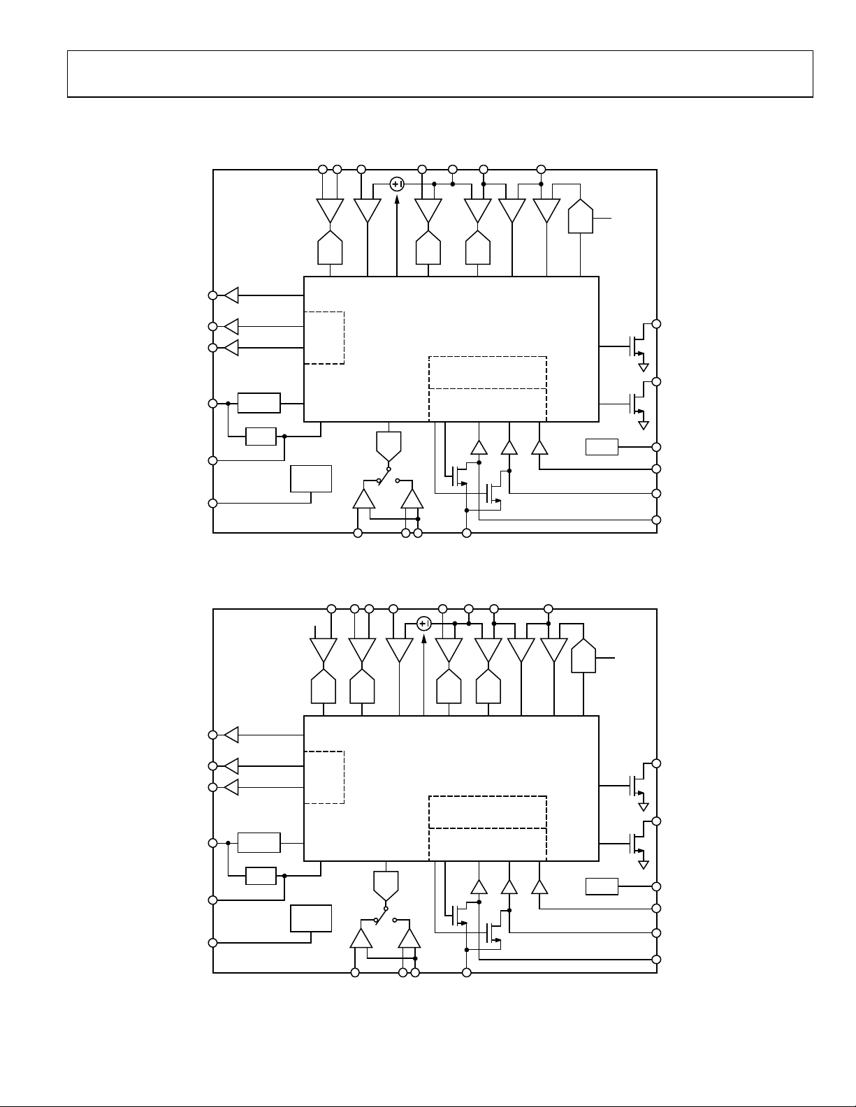
FUNCTIONAL BLOCK DIAGRAMS
CS+CS–
CILIM
FBPGND
OVP
ADP1047
–
INRUSH
PWM
PWM2
VDD
VCORE
RES
UVLO
LDO
ADC
CS OCP VAC VFB OLP OVP
PWM
ENGINE
VREF
ADC
ADC ADC
DIGITAL CORE
8kB EEPROM
INTERFACE
DGNDAGNDRTDADD
2
C
I
+
DAC
OSC
PGND
PGOOD
AC_OK
SYNC
PSON
SCL
SDA
09696-001
Figure 5. ADP1047 Functional Block Diagram
OVP
–
+
DAC
PGND
ADP1048
PGND
L
CS–
IB
CILIMCS+
FBPGND
INRUSH
PWM
PWM2
VDD
VCORE
RES
UVLO
LDO
PWM
ENGINE
VREF
ADC
ADC
CS OCP VAC VFB OLP OVP
CS
ADC
ADC ADC
DIGITAL CORE
8kB EEPROM
AGNDRTDADD
DGND
2
C
I
INTERFACE
OSC
PGOOD
AC_OK
SYNC
PSON
SCL
SDA
09696-002
Figure 6. ADP1048 Functional Block Diagram
Rev. 0 | Page 11 of 84
ADP1047/ADP1048 Data Sheet
CONTROLLER ARCHITECTURE
The ADP1047/ADP1048 integrate the following functions: The output of the Σ-Δ ADC is used for the following purposes:
• Power factor correction control loop (see the Power Factor
Correction Control Loop section)
• Advanced input power metering (see the Advanced Input
Power Metering section)
• PMBus digital communication (see the PMBus Digital
Communication section)
This section describes the internal architecture of the chip.
CURRENT SENSE
Current sensing is used for the control, protection, and monitoring of the PFC stage. For normal operation, the power factor
correction control loop requires inductor current information.
The typical implementation uses a sense resistor on the input
bus. A combination of two current transformers in series with
the power switch and the boost diode can be used to reconstruct
the inductor current and minimize losses in the resistive shunt,
but, in general, a good quality shunt resistor provides much
better accuracy in measuring input current and input power.
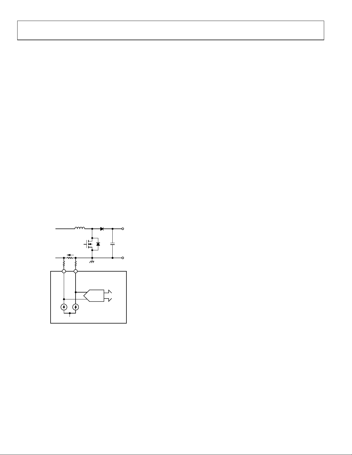
The inputs to the current sense ADC are differential. A pair of
matched current sources is provided to level shift the negative
signal across the current sense element in the input range of the
current sense ADC (see Figure 7).
• The output is decimated at the switching frequency for the
control loop. The effective number of bits (ENOB) is >7
when the current loop bandwidth is 10 kHz; the ENOB
is >10 when the current loop bandwidth is 1 kHz.
• The 11-bit result is calculated and updated at each half line
cycle for high accuracy ac line current and input power
monitoring and for overcurrent protection (accurate OCP).
RMS INPUT OVERCURRENT PROTECTION
The ADP1047/ADP1048 provide rms overcurrent protection
(OCP). RMS OCP (or accurate OCP) is distinct from the instantaneous pulse-by-pulse fast overcurrent protection and is based
on the rms value of the input ac current.
The measured value is compared to the limit set in the
IIN_OC_FAULT_LIMIT register (Register 0x5B) at the
end of each half cycle of the ac line. If the limit is exceeded,
the action programmed in the IIN_OC_FAULT_RESPONSE
register (Register 0x5C) is triggered.
In addition, an input current warning limit can be programmed
in the IIN_OC_WARN_LIMIT register (Register 0x5D). This
warning limit has no action attached to it, but it sets flags in the
STATUS_BYTE register (Register 0x78, Bit 0), the STATUS_WORD
register (Register 0x79, Bit 13), and the STATUS_INPUT register
(Register 0x7C, Bit 1).
I
L
10kΩ10kΩ
CS– CS+
+
–
ADP1047/ADP1048
VDD
Figure 7. Current Sense Configuration
11-B ITADC
09696-005
The current sense can be calibrated digitally to remove any
errors due to external components (see the Current Sense Gain
and Offset Trim section). This calibration can be performed in
the production environment; the settings are saved in the
EEPROM of the ADP1047/ADP1048.
FAST OVERCURRENT PROTECTION (ILIM PIN)
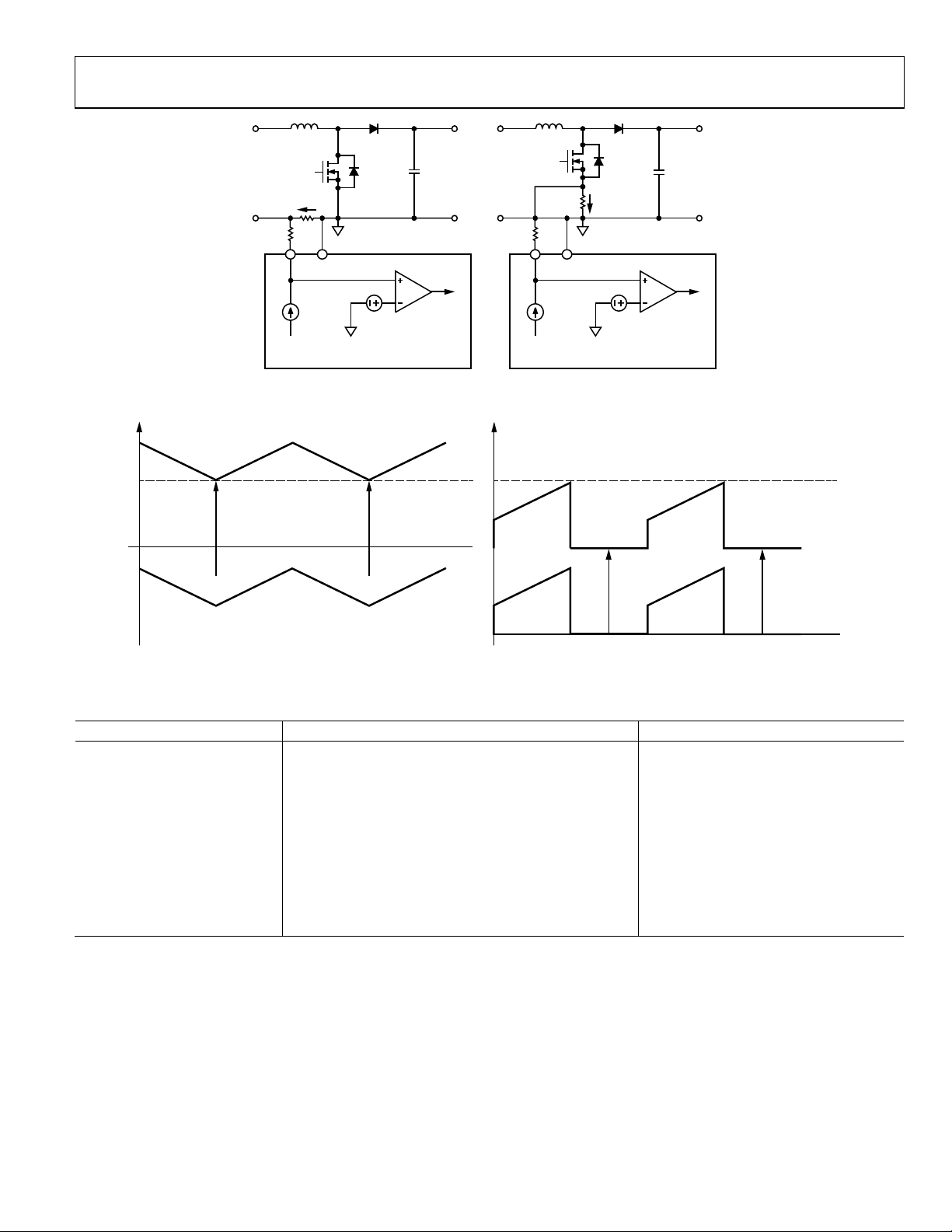
A dedicated current limiting pin (ILIM) is provided to protect
the part from pulse-by-pulse overcurrent events. When the
threshold is crossed, the PWM pulse is terminated. This action
is independent of any programming of the fast OCP flag. The
next switching cycle resumes normally. Additional actions can
be programmed (see Tabl e 5).
The OCP comparator on the ILIM pin can accept positive or
negative signals; the pin is referred to PGND (power ground) and
has programmable level shifting current sources (see Tab l e 5 ).
These sources can be changed during normal operation to adapt
to the level at which the overcurrent protection is triggered.
The OCP comparator also features programmable blanking and
debounce times (see Tabl e 5). If OCP is triggered, the PWM
signal is terminated and operation resumes at the next switching cycle unless a different action is specified for the fast OCP
response in Register 0xFE00.
Rev. 0 | Page 12 of 84
Data Sheet ADP1047/ADP1048
I
L
I
M
ILIM PGND
60µA TO
120µA
VDD
OCP
500mV
ADP1047/ADP1048
ILIM PGND
20µA TO
80µA
VDD
OCP
1500mV
ADP1047/ADP1048
9696-006
Figure 8. Fast Overcurrent Protection Schemes
500mV
0mV
LEVEL SHIFTING
10k × 120µA = 1.2V
Figure 9. Level Shifting and Threshold for OCP
1500mV
0mV
LEVEL SHIFTING
10k × 80µA = 0.8V
09696-007
Table 5. Programmable Options for Fast Overcurrent Protection
Parameter Values or Options Comments
Debounce Time 40 ns, 80 ns, 120 ns, 240 ns Register 0xFE3D, Bits[4:3]
Blanking Time 40 ns, 80 ns, 120 ns, 160 ns, 200 ns, 400 ns, 600 ns, 800 ns
Blanking from the leading edge;
Register 0xFE3D, Bits[2:0]
Propagation Delay 140 ns typical
Fixed value; does not include blanking or
debounce
Threshold Value and Polarity 500 mV (negative); 1500 mV (positive) Fixed values
Level Shifting Current Sources 60 A, 80 A, 100 A, 120 A (negative)
Register 0xFE3E, Bits[7:5]
20 A, 40 A, 60 A, 80 A (positive)
Actions for Fast OCP
Ignore (still terminates the PWM pulse); allow n switching
n = 1, 2, 4, 8; Register 0xFE00, Bits[7:6]
cycles, then shut down and soft start; allow n switching
cycles, then shut down and wait for PSON signal
Rev. 0 | Page 13 of 84
ADP1047/ADP1048 Data Sheet
V
V
CURRENT BALANCING (IBAL PIN, ADP1048 ONLY)
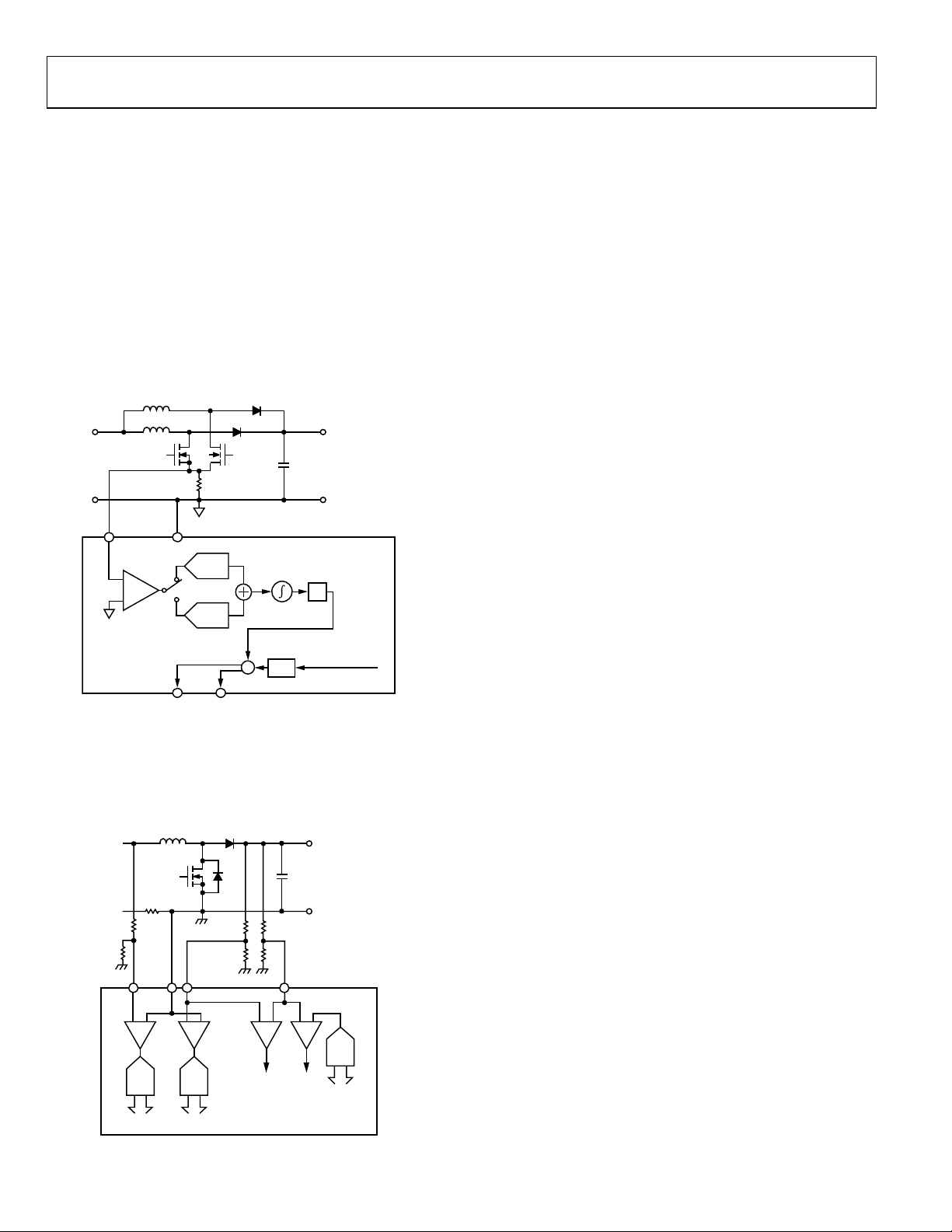
The ADP1048 has a dedicated circuit to maintain current balance
in each interleaved phase when operating in interleaved PFC
topology. This ensures that each interleaved phase provides equal
power regardless of the tolerance of the inductor and the boost
switch driving circuitry.
The input is through the IBAL pin specifically provided for the
ADP1048. The current balancing circuit monitors the current
flowing in both switches of the interleaved PFC topology and
stores this information. It compensates the PWM signals,
ensuring equal current flow to balance the current between
interleaved phases. Several switching cycles are required for
the circuit to operate effectively. The current balance settings
are programmed in Register 0xFE43 and Register 0xFE95.
The voltage sense can be calibrated digitally to remove any
errors due to external components (see the Output Voltage
(VFB) Calibration and Trim section). This calibration can
be performed in the production environment; the settings
are saved in the EEPROM of the ADP1047/ADP1048.
Input Voltage Sensing (VAC Pin)
The VAC pin is used for the monitoring and protection of the
rectified power supply input voltage. The sense point on the
power rail requires an external resistor divider to bring the signal
within the operating input range of the ADC (0 V to 1.6 V).
This scaled-down signal is fed into a high speed Σ-Δ ADC.
The output of the Σ-Δ ADC goes to the digital filter and is used
for the following purposes:
• The output is decimated at the switching frequency for the
control loop. The effective number of bits (ENOB) is >7
when the current loop bandwidth is 10 kHz; the ENOB
is >10 when the current loop bandwidth is 1 kHz.
• The 11-bit result is calculated and updated at each half line
cycle for high accuracy input voltage and power monitoring.
IBAL
ADP1048
PGND
0° TO 180°
ADC
+
–
ADC
180° TO 360°
PWM PWM2
Figure 10. Current Balancing (IBAL) for the ADP1048
PWM
K
OUTPUT OF PFC
CURRENT LOOP
09696-008
VOLTAGE SENSE
Voltage sensing is used for the control, protection, and monitoring of the PFC stage. Input and output voltages are sensed using
dedicated ADCs and references (see Figure 11).
REC
VAC P GND VF B
–
+
ADC
11-BIT
Figure 11. Typical Voltage Sense Configuration
+
ADC
11-BIT
–
OUT
OVP
–
+
DAC
OVPOLP
7-BIT
ADP1047/ADP1048
09696-009
Rev. 0 | Page 14 of 84
Output Voltage Sensing (VFB Pin)
The VFB pin is used for the control, monitoring, and protection
of the output voltage. This voltage is the main feedback loop for
the power supply control loop. The sense point on the power rail
requires an external resistor divider to bring the signal within the
operating input range of the ADC (0 V to 1.6 V). This scaleddown signal is fed into a high speed Σ-Δ ADC.
The output of the Σ-Δ ADC goes to the digital filter and is used
for the following purposes:
• The 11-bit result is used at each half line cycle for the
normal control loop to control the value of the output
voltage.
• The 10-bit, 1.5 kHz update rate is used for the fast voltage
control loop to control the value of the output voltage
during large transients.
To reduce the current distortion from the output voltage feedback, a prefilter is implemented before the voltage loop filter.
The prefilter detects the zero-crossing point of the input voltage
to identify the half input line cycle. The prefilter then performs
an averaging function for the sampled VFB signal during this
half line cycle. In this way, the fundamental frequency of the
output bulk voltage ripple and its harmonics are significantly
attenuated.

Data Sheet ADP1047/ADP1048
OVERVOLTAGE PROTECTION
The ADP1047/ADP1048 have two OVP circuits: an ADC-based
comparator and a fast comparator.
Accurate Overvoltage Protection (VFB Pin)
Overvoltage protection (OVP) is implemented using the information available on the output of the VFB ADC. The information
from the VFB ADC is averaged over one half the ac line frequency;
therefore, the response of this OVP is relatively slow.
The threshold for the accurate OVP is fully programmable
using the VOUT_OV_FAULT_LIMIT register (Register 0x40).
The programmed value is the dc average voltage.
When the accurate OVP threshold is crossed, the accurate OVP
flag is set. The response to this flag can be programmed for one
of several actions using the VOUT_OV_FAULT_RESPONSE
register (Register 0x41). If the disable PWM option is selected,
a voltage hysteresis can be programmed for the accurate OVP
threshold using Register 0xFE50.
Table 6. Programmable Options for Fast Overvoltage Protection (Fast OVP)
Parameter Values or Options Comments
Debounce Time 120 ns, 240 ns, 480 ns, 640 ns
Blanking Time 10 s (fixed)
Propagation Delay 120 ns max (fixed) Does not include blanking or debounce
Threshold Rising 1 V to 1.5 V Programmable using Register 0xFE2F, Bits[6:0]
Threshold Falling 1 V to 1.5 V Programmable using Register 0xFE30, Bits[6:0]
Actions for Fast OVP
Immediate shutdown and wait for PSON;
disable PWM until the flag is cleared;
shut down and soft start; ignore (do nothing)
Fast Overvoltage Protection (OVP Pin)
A fast OVP mode is implemented using a programmable
comparator on the OVP pin. Fast OVP is used for overvoltage
protection of the bulk capacitors and to provide open-loop
protection. The sense point on the power rail requires an
external resistor divider to match the divider applied to VFB.
This separate divider introduces a level of redundancy in
sensing the output voltage to improve system reliability.
If the voltage divider on the VFB pin is damaged or drifts in
value, the OVP pin can still detect an overvoltage condition
and take the appropriate programmed action.
The fast OVP signal is fed into a comparator with a programmable threshold to set the trip point for overvoltage. The
threshold is set using a DAC.
Minimum duration of pulse to be considered;
programmable using Register 0xFE31, Bits[1:0]
Duration of time while the comparator is blanked
and the threshold changes from rising to falling
Register 0xFE01, Bits[7:6]
Rev. 0 | Page 15 of 84
ADP1047/ADP1048 Data Sheet
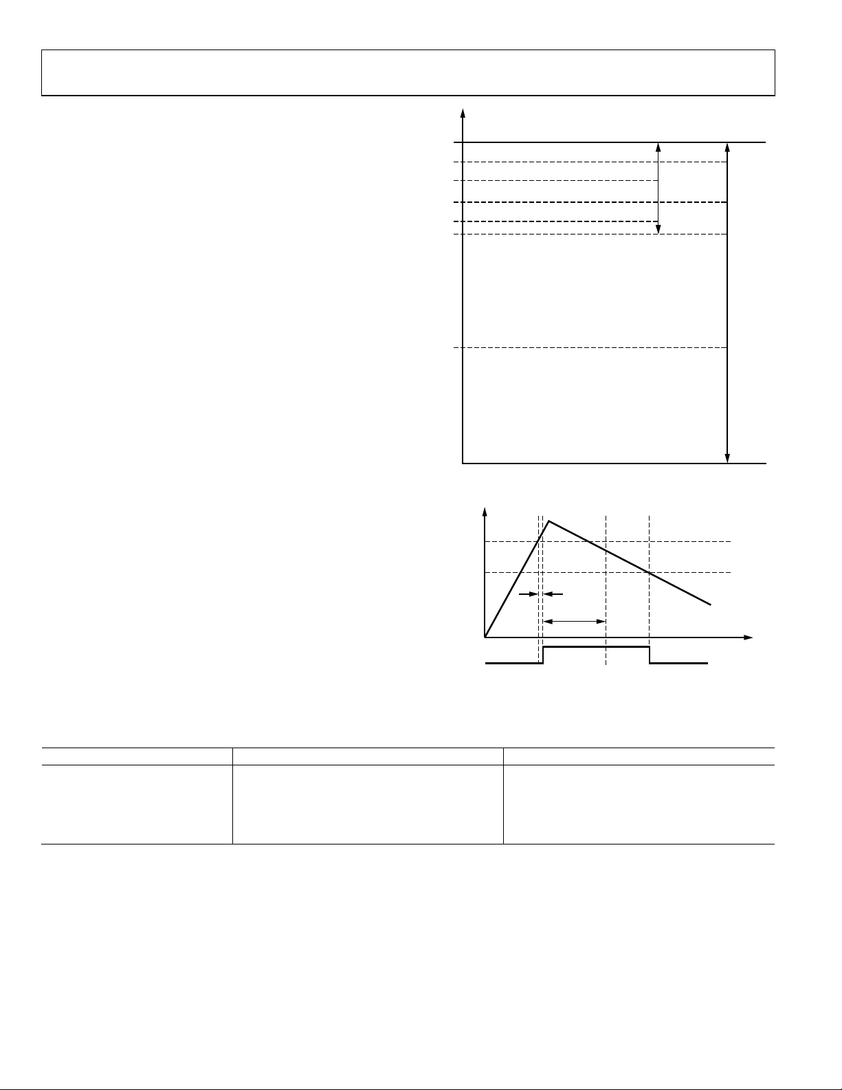
Figure 12 shows an example of the output voltage and the OVP
thresholds set. The rising and falling thresholds, FAST_OVP_
FAULT_RISE and FAST_OVP_FAULT_FALL, respectively, are
used for fast OVP protection. FAST_OVP_FAULT_RISE
corresponds to OVP
, which is the trip point for overvoltage
UP
protection (see Figure 13). FAST_OVP_FAULT_FALL corresponds to OVP
, which is the reset point for the fast OVP.
DOWN
When the rising threshold is triggered, the programmed action
is applied and the threshold is switched to the programmed falling threshold (if the programmed falling threshold is different
from the rising threshold).
A blanking time is applied when the thresholds are switched to
avoid spurious signals (see the timing diagram in Figure 13). A
programmable debounce time is applied to the OVP signal as
well to avoid false triggering.
The rising and falling thresholds are programmable from 1 V
to 1.5 V (at the OVP pin) using Register 0xFE2F and Register
0xFE30, respectively.
Open-Loop Protection
Open-loop protection detects differences between the OVP and
VFB pins. Identical resistor dividers are applied to these pins;
therefore, if a voltage difference is present, it means that one or
more resistors in the dividers have the wrong values or are not
connected. In this case, it is usually recommended that the user
shut down the system to prevent damage.
The open-loop protection detects a difference in voltage in
excess of ~100 mV, which equates to approximately 6.6% of
the full-scale range.
A debounce time of 10 μs is added to avoid false triggering. If
filtering capacitors are applied to the OVP and VFB pins, care
must be taken to make sure that the time constant difference
does not exceed 10 μs.
Table 7. Programmable Options for Open-Loop Protection (OLP)
Parameter Values or Options Comments
Debounce Time 10 s (fixed) Minimum duration of pulse to be considered
Propagation Delay 200 ns (fixed) Does not include debounce
Actions for OLP
Immediate shutdown and wait for PSON;
disable PWM until the flag is cleared;
shut down and soft start; ignore (do nothing)
ADC INPUT RANGE = 1.6V
1.6V
1.0V
0.5V
VOUT_OV_FAULT_LIMIT = 450V (REG 0x40)
FAST_OVP_FAULT_RISE = 435 V (REG 0xFE 2F)
VOUT_OV _WARN_LIMIT = 420V (REG 0x42)
FAST_OVP_FAULT_FALL = 400V (REG 0xFE30)
VOUT_COM MAND = 385V (REG 0x21)
VOUT_UV_FAULT_LIMIT = 200V (REG 0x44)
Figure 12. Output Voltage Levels
OUTPUT
VOLTAGE
DOWN
FLAG
OVP PIN
UP
DEBOUNCE
10µs
Figure 13. OVP Thresholds and Timing
OVP
OVP
OVP
Register 0xFE02, Bits[7:6]
FAST OVP
PROGRAMMING
RANGE
TIME
ADC
FULL
RANGE
09696-020
09696-021
Rev. 0 | Page 16 of 84
Data Sheet ADP1047/ADP1048
V
POWER FACTOR CORRECTION CONTROL LOOP
The ADP1047/ADP1048 implement the average current mode
power factor correction control loop using a traditional multiplier approach. The implementation of the loop is digital, and
all the signals are converted from analog to digital before they
are processed by the control loop. Σ-Δ ADCs are used to achieve
high performance, cost-effective implementation. Each ADC
has its own dedicated voltage reference.
DIGITAL COMPENSATION FILTERS
The ADP1047/ADP1048 are digital PFC controllers with ac power
monitoring. They are implemented in the digital domain using
a dedicated state machine, which allows the user to program the
loop response specifically, with no need for external loop
compensation.
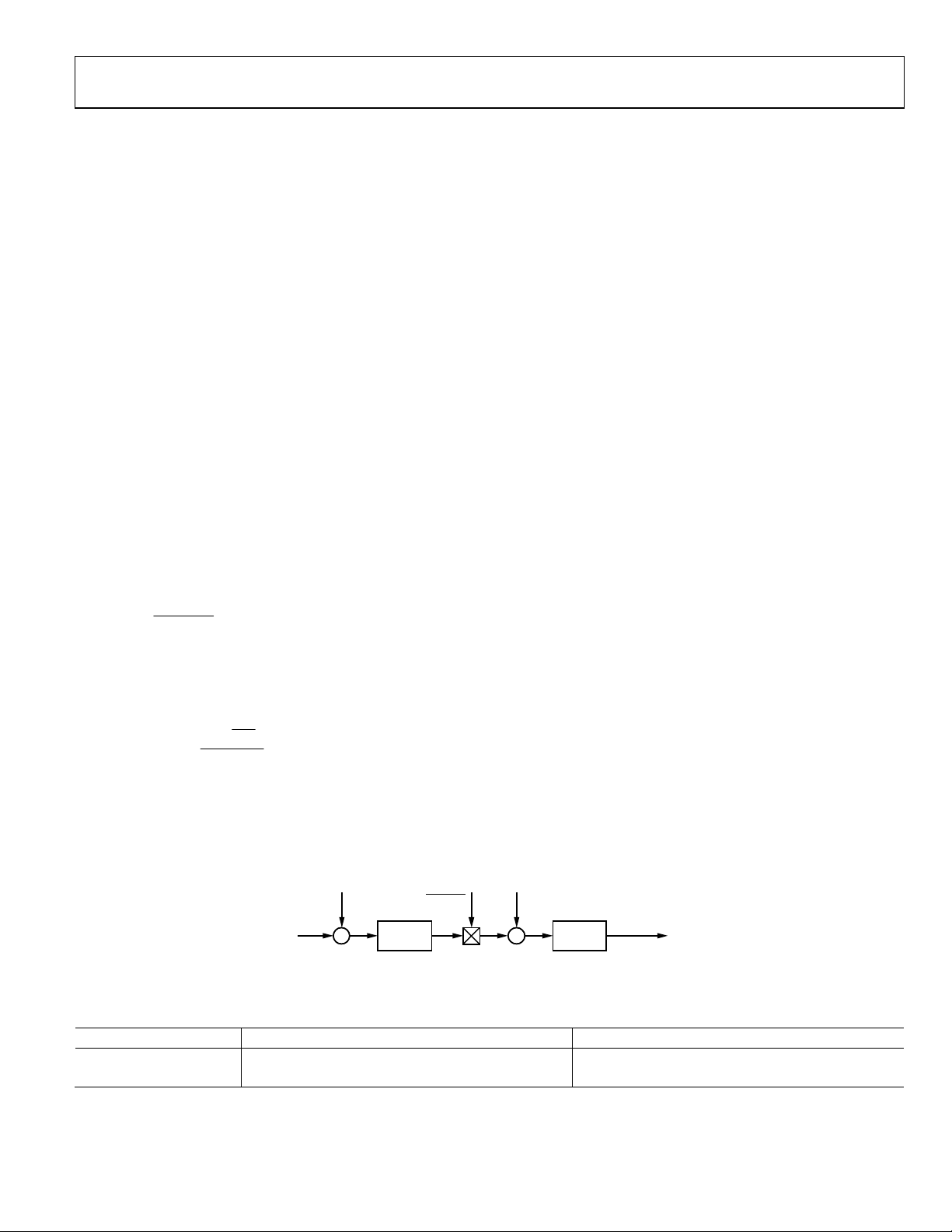
The detailed control loop configuration is illustrated in Figure 14.
V
is the digital reference voltage setting; VFB is the sensed feed-
REF
back voltage of the output. The difference between V
is processed first by the voltage loop filter (H
). Its output, VEA,
V
is then multiplied by the instantaneous rectified input voltage,
V
, and divided by the square of the rms value of VAC. The result,
AC
I
, is used as the reference signal for the current. The output of
REF
the current loop filter (H
) is the duty cycle command. The
I
mathematical expression is
VVI×
REF
=
ACEA
2
V
_ RMSAC
Both the voltage loop and current loop digital compensating
filters, H
(z) and HI(z), are programmable. The filter transfer
V
function in the digital domain is
a
⎛
z
⎜
⎝
××=
bkH(z)
⎞
−
⎟
256
⎠
()
1
−
z
where:
a is the filter zero.
b is the filter gain.
k is related to the switching frequency.
V
FB
–
V
+
REF
and VFB
REF
AC
2
V
AC_RMS
HV(z)
V
EA
Figure 14. Control Loop Digital Filters
The frequency gains and zero locations can all be programmed
individually to tailor the loop response to the application. It is
recommended that the Analog Devices, Inc., GUI software be
used to program the filter (see the Software GUI section). The
GUI displays the filter response in Bode plot format and can be
used to calculate all stability criteria for the power supply.
Optimized Compensation Filters
Instead of a single programmable compensation filter, the
ADP1047/ADP1048 offer the following filter presets so that
the dynamic response of the control loop can be tailored to
optimize different operating conditions.
•
Low line current filter
High line current filter
•
Fast voltage compensation filter
•
The ADP1047/ADP1048 can be configured to switch automatically between the high and low line filters when the rms
value of the ac line crosses the programmed threshold between
the high and low lines. (The high line threshold is programmed
in Register 0xFE35; the low line threshold is programmed in
Register 0xFE36.)
The ADP1047/ADP1048 check for the value of the rms input
voltage at each half line cycle. When a transition between the
high and low line threshold is detected, the part waits for four
full line cycles before switching to the correct filter at the zero
crossing of the input line cycle. This is done to avoid spurious
transitions due to a missing or distorted voltage line cycle.
During soft start, one of four combinations of filters can be
used, depending on whether the fast loop mode is enabled
and whether the high line or low line is detected for soft start
(see Tabl e 8).
I
L
–
I
REF
+
HI(z)
DUTY CYCLE
09696-010
Table 8. Summary of the PFC Digital Compensation Filters for Soft Start
Line Filter Normal Compensation Filter Fast Voltage Compensation Filter
High Line High line current filter, normal voltage filter High line current filter, fast voltage filter
Low Line Low line current filter, normal voltage filter Low line current filter, fast voltage filter
Rev. 0 | Page 17 of 84
ADP1047/ADP1048 Data Sheet
Fast Loop Mode
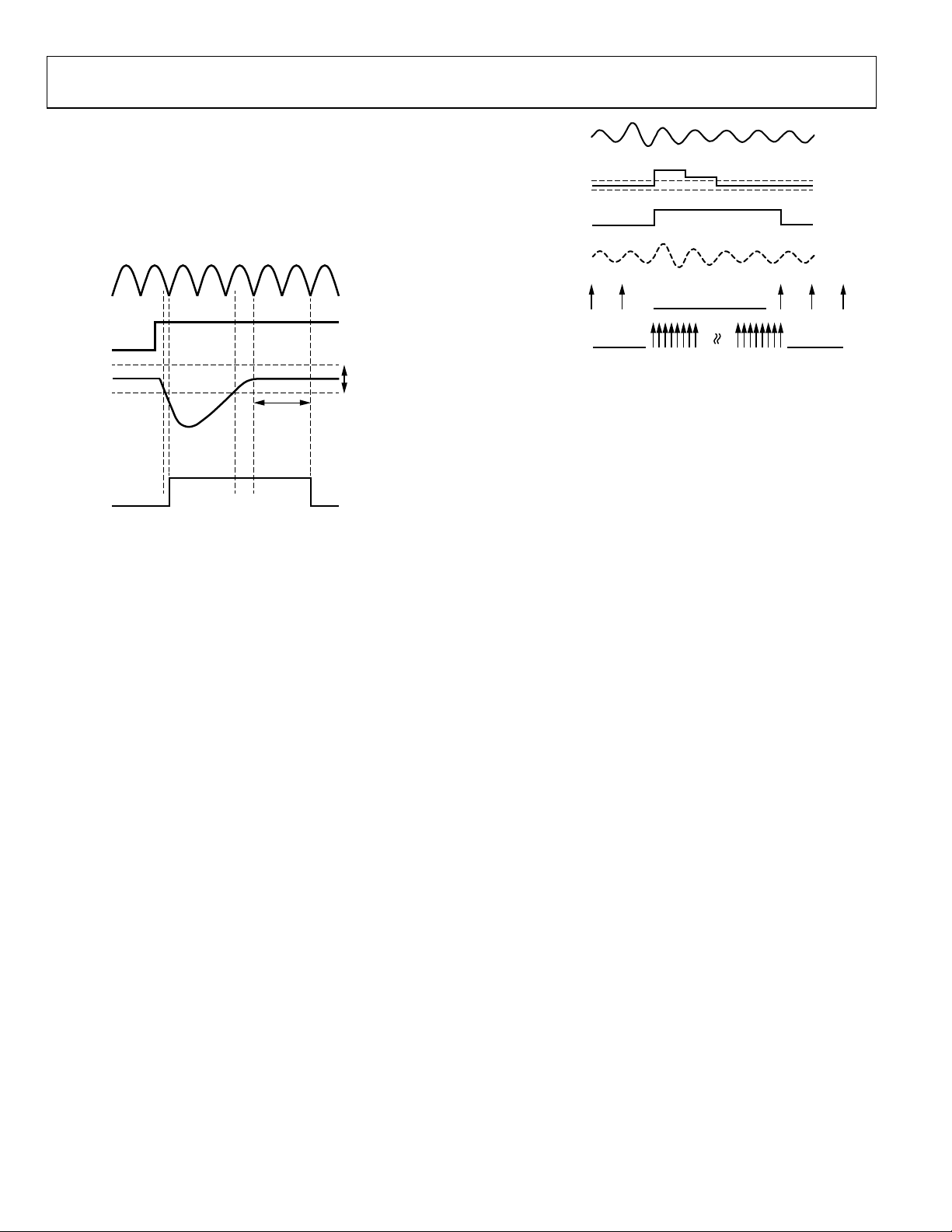
During transients, a fast loop mode is enabled to allow for faster
loop responses. Typical timing can be seen in Figure 15. The
fast loop mode has separate settings and can be programmed to
respond quickly to load transients. The user can disable the fast
loop mode if it is not required by the application.
V
REC
I
LOAD
PROGRAMMABLE
RANGE
V
OUT
FAST L OO P
Figure 15. Fast Loop for Transient Response Improvement
PROGRAM-
MABLE
DELAY
(0 TO 7
HALF LINE
CYCLES)
When fast loop mode is enabled and the feedback output voltage
is out of range from the desired reference value (programmable
band of 1.5%, 3%, 6%, or 12%, set in Register 0xFE24), the
ADP1047/ADP1048 enter fast loop mode.
To ensure a smooth transition, the ADP1047/ADP1048 switch
from the regular filter to the fast loop filter at the zero crossing
of the rectified input voltage. When the output voltage returns
to regulation within the programmed band, the controller
switches back (after a programmable delay of 0 to 7 half line
cycles) to the normal loop at the next zero crossing of the
rectified input voltage.
If the output voltage does not return to regulation within the
programmed band after a fixed time of 630 ms, the control loop
automatically switches back to the normal loop.
In the normal compensation loop, the sampling frequency of
the output voltage is the same as the ripple oscillation frequency
(which is commonly 100 Hz or 120 Hz).
During fast loop operation, the feedback voltage is sampled
at 1.5 kHz, and the fast filter is applied to regulate the output
voltage. The output voltage is averaged and decimated at
1.5 kHz (see Figure 16).
Rev. 0 | Page 18 of 84
VFB
VFB ERROR
FAST LO OP
VFB FAST ERROR
NORMAL FILTER
@ 100Hz
FAST FI LTER
@ 1.5kHz
Figure 16. Fast Loop Operation
09696-012
Based on the requirements of the application, the user can enable
or disable the fast loop mode by programming Register 0xFE24.
It is recommended that fast loop mode be enabled for the
ADP1047/ADP1048 during large load transients. The fast loop
mode settings are also used during soft start, even when the fast
loop is disabled.
09696-011
PULSE-WIDTH MODULATION
The ADP1047/ADP1048 can implement either leading edge or
trailing edge modulation. Trailing edge modulation is the more
popular modulation scheme. Using trailing edge modulation,
the rms ripple current in the bulk capacitors can be reduced
when used with downstream converter synchronization. It is
recommended that the Analog Devices, Inc., GUI software be
used to program PWM (see the Software GUI section).
DUTY CYCLE MINIMUM/MAXIMUM LIMITS
The ADP1047/ADP1048 allow the user to program the mini-
mum off time and the minimum on time for the PWM outputs
separately, thereby allowing the minimum and maximum duty
cycles to be set.
The minimum off time represents the minimum time that the
PWM is low during each switching cycle. It can be programmed
from 40 ns to 1.2 μs in steps of 80 ns using Register 0xFE15,
Bits[3:0]. In this way, the maximum duty cycle can be clamped
between 96% and 99.8% at the minimum frequency and
between 48.8% and 96.8% at the maximum frequency.
The minimum on time is the smallest PWM pulse that the modulator generates on the PWM output. It can be programmed
from 0 ns to 1200 ns in steps of 80 ns using Register 0xFE15,
Bits[7:4].
AUXILIARY PWM OUTPUT (ADP1047 ONLY)
For the ADP1047, the PWM2 pin is the output for the auxiliary
PWM, which can be independent of the main PWM output.
PWM2 can be used as the control signal for auxiliary switching
in the zero-voltage transition soft-switched PFC boost circuit.

Data Sheet ADP1047/ADP1048
SWITCHING FREQUENCY PROGRAMMING
The switching frequency of the PWM outputs can be programmed from 30 kHz to 400 kHz using Register 0xFE1B, Bits[5:0] (see Tab l e 9).
Table 9. Switching Frequency Settings from 30 kHz to 400 kHz (Register 0xFE1B, Bits[5:0])
Frequency
Setting
(Decimal)
0 30.05 16 107.76 32 204.92 48 277.78
1 32.55 17 111.61 33 208.33 49 284.09
2 35.51 18 115.74 34 211.86 50 290.70
3 39.06 19 120.19 35 215.52 51 297.62
4 43.40 20 125.00 36 219.30 52 304.88
5 48.83 21 130.21 37 223.21 53 312.50
6 52.06 22 135.87 38 227.27 54 320.51
7 55.80 23 142.05 39 231.48 55 328.95
8 60.10 24 148.81 40 235.85 56 337.84
9 65.10 25 156.25 41 240.38 57 347.22
10 71.02 26 164.47 42 245.10 58 357.14
11 78.13 27 173.61 43 250.00 59 367.65
12 86.81 28 183.82 44 255.10 60 378.79
13 97.66 29 195.31 45 260.42 61 390.63
14 100.81 30 198.41 46 265.96 62 403.23
15 104.17 31 201.61 47 271.74 63 403.23
Frequency
(kHz)
Frequency
Setting
(Decimal)
Frequency
(kHz)
Frequency
Setting
(Decimal)
Frequency
(kHz)
Frequency
Setting
(Decimal)
Frequency
(kHz)
Rev. 0 | Page 19 of 84
ADP1047/ADP1048 Data Sheet
LINE FAULT PROTECTIONS AND SOFT START SEQUENCING
PSON OPERATION
To comply with PMBus standards, the PFC circuit controlled
by the ADP1047/ADP1048 can be turned on and off by the
hardware PSON pin and/or the software PSON command. The
setting of Bit 2 in Register 0x02 determines whether the PSON
pin and/or the PSON command is used. If the PSON pin is used,
the pin can be configured to be either active high or active low
(see Tabl e 18).
AC LINE DETECTION
The ADP1047/ADP1048 are capable of detecting several
parameters of the ac line input voltage and taking the appropriate programmed actions when necessary. The detection is
a combination of time and voltage measurements and is
implemented via the VAC pin, which detects the rectified ac
input voltage. This allows early detection of ac line faults and
early warning for the host system, thereby increasing reliability.
Five main parameters are related to ac line detection.
•
VAC_LINE_PERIOD (Register 0xFE85)
VAC_THRESHOLD_SET (Register 0xFE25)
•
VAC_THRESHOLD_READ (Register 0xFE26)
•
MIN_AC_PERIOD_SET (Register 0xFE27)
•
MAX_AC_PERIOD_SET (Register 0xFE28)
•
AC Line Period and Zero Crossing
The input ac line period is measured every half period of the ac
line cycle and is reported in the VAC_LINE_PERIOD register
(Register 0xFE85).
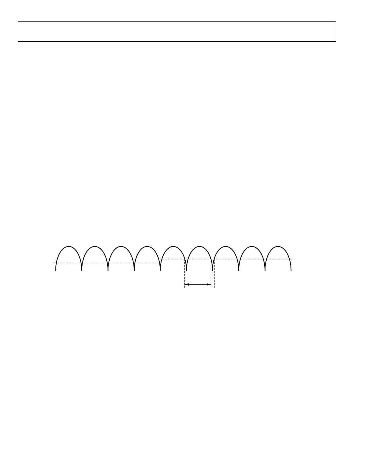
During the first 40 ms, the ac line period is measured between
two consecutive falling crossings of the threshold value, which
is set in the VAC_THRESHOLD_SET register (Register 0xFE25,
Bits[6:0]). The ac line period is then measured between two
consecutive falling crossings and compared to the average value
of the input line voltage, which is calculated during each half line
period. The VAC average reading can be found in the VAC_
THRESHOLD_READ register (Register 0xFE26, Bits[6:0]).
If the measured period is larger than MAX_AC_PERIOD_SET
or smaller than MIN_AC_PERIOD_SET, the default, MAX_AC_
PERIOD_SET, is used as the value of the period.
As shown in Figure 17, the two consecutive crossing points,
B and C, are used to determine the zero-crossing point of the
ac line. The middle point between B and C is calculated as the
zero-crossing point.
This information is used by the control loop, as well as the
power metering block.
THRESHOLD
(REG 0xFE2 5)
VAC
ABC
HALF AC
LINE PERIO D
Figure 17. AC Line Period Detection
VAC AVERAGE
(REG 0xFE 26)
09696-013
Rev. 0 | Page 20 of 84
Data Sheet ADP1047/ADP1048
V
AC Line Value Detection
To operate, the controller must detect the ac line value. At
startup, the controller waits for the PSON signal (hardware
PSON, software PSON, or both, depending on how the part
is programmed).
When the PSON signal is present, the controller looks for the
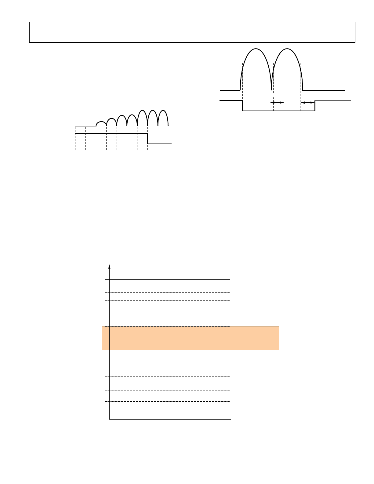
ac line period and value (see Figure 18).
IN_ON (REG 0x35)
VAC
BROWN_OUT F LAG
(REG 0xFE 80[2])
09696-014
Figure 18. VAC Detection for Startup
The start-up value for the ac line used by the controller to
initiate the start-up procedure is stored in the VIN_ON register
(Register 0x35). This value is the minimum rms value of the ac
line required for the system to start up. The controller measures
the value of VAC at every half line cycle and compares it with
VIN_ON. If VAC is larger than the value in the VIN_ON register,
the soft start procedure is initiated and the BROWN_OUT flag
is reset.
AC Line Early Fault Detection
After the VIN_ON limit is crossed and the system starts up, the
controller constantly monitors the condition of the ac line (see
Figure 19).
VAC
VIN_OFF (REG 0x36)
TIMER
1/4
VIN_LOW FLAG
(REG 0x7C[3])
TIMER
1/4
Figure 19. AC Line Early Fault Detection
To provide early detection of ac line faults, the instantaneous
value of VAC is compared to the VIN_OFF value in Register
0x36. If VAC remains below the VIN_OFF threshold for a time
longer than the programmed period, the VIN_LOW flag is set
in Register 0x7C. The programmed period can be either a fraction of the detected ac line period (one-quarter or one-half) or
it can be an absolute time (2 ms or 4 ms); the value is set in
Register 0xFE2E.
The controller does not take any action, but the VIN_LOW
signal can be used to set the AC_OK signal and to trigger
immediate actions in the power system.
The VIN_OFF threshold is intended solely to provide early
warning of problems on the ac line; it is not used to shut down
the power supply. The VIN_UV_FAULT_LIMIT register
(Register 0x59) is used for that purpose.
09696-015
ADC INPUT RANGE = 1.6V
VIN_OV_FAULT_LI MIT = 270VAC (REG 0x55)
VAC
= 265V
HIGH LINE LIMIT (VAC
LOW LINE LIMIT (VAC
VIN_ON = 85V
VIN_UV_WARN_LIM IT = 80V
VIN_OFF = 70V
VIN_UV_FAULT_LIM IT = 70V
TH
TH
) = 180V (REG 0xFE35)
) = 150V (REG 0xFE36)
(REG 0x35)
AC
(REG 0x58)
AC
(REG 0x36)
AC
(REG 0x59)
AC
VAC
MAX
MIN
HYSTERESIS
= 90V
AC
AC
ZONE
09696-016
Figure 20. Input Voltage Limits
Rev. 0 | Page 21 of 84

ADP1047/ADP1048 Data Sheet
V
SOFT START PROCEDURE
The PSON signal is used to enable or disable the PFC stage.
After PSON is asserted, the ADP1047/ADP1048 start monitoring VAC and, if the ac line conditions are met, they initiate the
soft start procedure, as shown in Figure 21.
Startup is gated by the rms value of the ac line voltage measured
on one half period of the ac line frequency. When VAC is above
the VIN_ON value, the BROWN_OUT flag is reset and the soft
start sequence is initiated. At the same time, the inrush delay
time and soft start delay time timers begin. Both of these timers
can be programmed to count 0 to 7 line cycles (or 0 to 14 half
line cycles in steps of 2).
After the inrush delay time programmed in Register 0xFE2E,
Bits[2:0], the INRUSH flag is reset and the inrush signal (Pin 17)
is asserted, closing the inrush current relay. (Note that the INRUSH
flag is active low.) The inrush signal is set at the zero crossing of
the ac voltage, if this crossing is detected. This setting allows
zero voltage turn-on if a solid-state switch is used (zero voltage
turn-on is not relevant with mechanical relays).
After the soft start delay time (programmed in Register 0xFE2D,
Bits[5:3]), the output voltage is ramped up according to the soft
start time programmed in Register 0xFE2D, Bits[2:0].
Some of the flags can be blanked during soft start so that the
programmed action of the flag does not take place if the flag
is set during the soft start period (see Register 0xFE08 and
Register 0xFE09).
IN_ON (REG 0x35)
VIN_OFF (REG 0x36)
VAC
When output voltage regulation is reached and all flags are OK, the
POWER_GOOD# flag is reset and the PGOOD signal (Pin 16)
is set to Logic Level 1. (Note that the POWER_GOOD# flag is
active low.)
The soft start time can be programmed to one of eight values:
112 ms, 168 ms, 224 ms, 280 ms, 392 ms, 504 ms, 616 ms, or
728 ms (set in Register 0xFE2D, Bits[2:0]).
The soft start delay time (Register 0xFE2D, Bits[5:3]) can be
programmed from 0 to 7 full line cycles in increments of 1
(that is, two of the rectified half line cycles).
The inrush delay time (Register 0xFE2E, Bits[2:0]) can be programmed from 0 to 7 full line cycles in increments of 1 (that is,
two of the rectified half line cycles).
If no zero crossings are detected, the programmed maximum ac
line period, MAX_AC_PERIOD_SET (Register 0xFE28), is used.
LINE FAULT PROTECTIONS
Line faults occur when the ac line is not behaving correctly
and include anomalies such as a missing ac line cycle (can be
partial), brownout, or high distortion levels. When a line fault
occurs, the ADP1047/ADP1048 can be programmed to react
according to the situation.
VIN_LOW FLAG
(REG 0x7C[3])
BROWN_OUT F LAG
(REG 0xFE8 0[2])
INRUSH PIN
VOUT
Figure 21. Soft Start and Inrush Current Control Timing
INRUSH
DELAY TIME = 2
(REG 0xFE 2E[2:0])
SOFT START
DELAY TIME = 3
(REG 0xFE2D[5:3])
SOFT START TIME
(REG 0xFE2D[2:0])
09696-017
Rev. 0 | Page 22 of 84
Data Sheet ADP1047/ADP1048
V
Missing AC Line Cycles
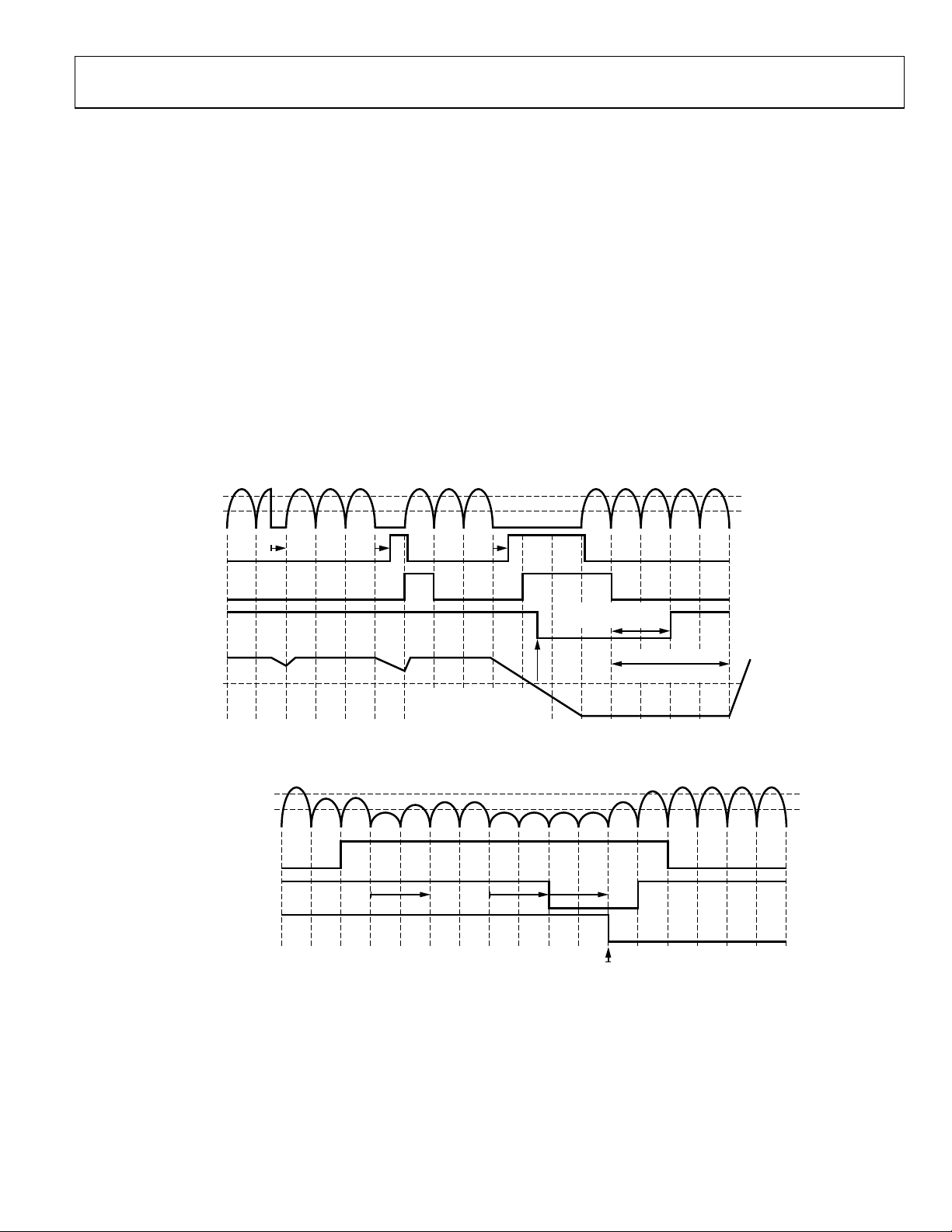
Figure 22 shows examples of the typical missing ac line cycles
fault. The VIN_LOW flag is set when the instantaneous voltage
is below VIN_OFF for more than a quarter or half line cycle
(depending on how it is programmed). This flag can be used as
an early warning to the system via the AC_OK pin when more
than a half cycle is missing. The BROWN_OUT flag is also set;
this flag does not cause a shutdown.
If any other flag that is programmed for shut down is set (in this
example, VOUT_UV_FAULT), the power supply shuts down,
the INRUSH pin is asserted, and the controller prepares for the
next soft start cycle.
If the BROWN_OUT flag is cleared before VOUT drops below
the VOUT_UV_FAULT_LIMIT value (Register 0x44), operation resumes in normal mode (or fast loop mode if enabled);
otherwise, if VOUT drops below VOUT_UV_FAULT_LIMIT,
the INRUSH pin is reset and a new soft start cycle is started.
VAC
PSON Delay
The PSON start delay is programmable using Register 0xFE06,
Bits[3:2]. Four options are available: 0 ms, 50 ms, 250 ms, and
1000 ms.
Brownout Conditions
Brownout is another typical line fault condition in which the
line drops below the minimum specified operating level. This
level can be set with VIN_UV_FAULT_LIMIT (Register 0x59).
This flag can be programmed according to the standard PMBus
flag response. For example, it can be programmed to shut down
and restart after a certain delay.
During brownout, there are other conditions that can occur,
such as input overcurrent or output undervoltage. Each of these
faults can be programmed to shut down or disable the output,
based on the response action.
VIN_ON (REG 0x35)
VIN_OFF (REG 0x36)
VIN_LOW FLAG
(REG 0x7C[3])
BROWN_OUT F LAG
(REG 0xFE80[ 2])
INRUSH DELAY TIME
INRUSH PIN
VOUT
VOUT_UV_FAULT_LIMIT
Figure 22. Line Fault (Missing Cycles) Timing Diagram
(REG 0x44)
(REG 0xFE2E [2:0])
SOFT START TIME
(REG 0xFE2D[2:0])
09696-018
AC
VIN_ON (REG 0x35)
VIN_UV_FAULT_LIM IT
(1 CYCLE DEBOUNCE)
Figure 23. Brownout Timing Diagram (VIN_UV_FAULT_RESPONSE Register Programmed to Shut Down After a One-Cycle Debounce)
(REG 0x59)
BROWN_OUT F LAG
(REG 0xFE80 [2])
VIN_UV_ FAULT FLAG
INRUSH PIN
SHUTDOWN
09696-019
Rev. 0 | Page 23 of 84
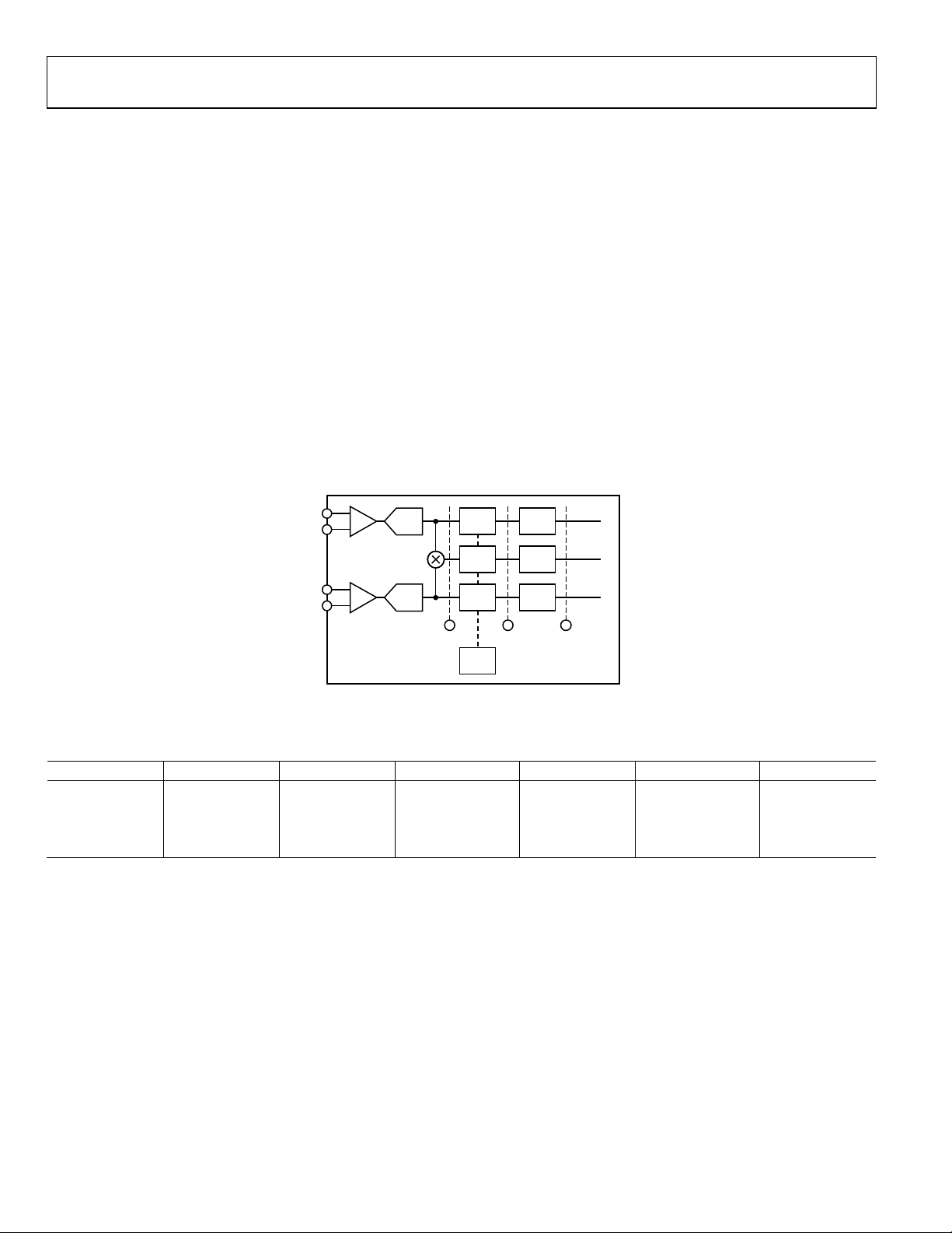
ADP1047/ADP1048 Data Sheet
ADVANCED INPUT POWER METERING
The ADP1047/ADP1048 monitor and communicate critical
information, including input and output voltage, input and
output current, temperature, and efficiency. They also monitor
a n d c om mu ni c at e O VP, U V P, O CP, OT P, an d o p e n -l oo p pr ot ec tion functions. An I
2
C interface reads all these values and flags
and programs their thresholds. The on-chip EEPROM can be
used to store all of the settings for the thresholds.
True rms values are calculated at the end of each half ac line
cycle by integrating the instantaneous values across each line
cycle. These values have a resolution of 11 bits and are used to
calculate the average, but are not available to be read through
the PMBus interface.
The averaging window is programmable from zero full line
cycles to 4096 full line cycles using Register 0xFE3A. At the
end of each averaging period, the new value for average power
is written to the READ_PIN register (Register 0x97) and is
available to be read back through the interface until it is
overwritten by the next averaged value at the end of the next
averaging period.
For this reason, the polling frequency used to read average
power through the PMBus interface must be equal to or higher
than the averaging window to maintain data integrity. The
averaging window is programmable over a wide range of times
to accommodate different situations.
Input voltage, input current, output voltage, and input power
are reported in linear format in the following registers:
•
Input voltage: READ_VIN (Register 0x88)
Input current: READ_IIN (Register 0x89)
•
Output voltage: READ_VOUT (Register 0x8B)
•
Input power: READ_PIN (Register 0x97)
•
VAC
PGND
CS+
CS–
ADC AVG
ADC AVG
Figure 24. Block Diagram of Power Monitoring
RMS
RMS
RMS
1 2 3
AC
SYNC
AVG
0 LINE CYCLES
TO 4096
LINE CY CLES
V
IN
P
IN
I
IN
09696-022
Table 10. Data Format and Range for VIN, IIN, PIN, and V
OUT
Metering Data Mantissa (Bits) Exponent (N) Minimum Range Minimum LSB Maximum Range Maximum LSB
VIN 11 −3 to −1 256 V 0.125 V 1024 V 0.5 V
IIN 11 −10 to −5 2 A 0.976 mA 64 A 0.03125 A
PIN 11 −4 to +3 256 W 125 mW 32.8 kW 16 W
V
11 −3 to 0 256 V 0.125 V 2048 V 1 V
OUT
Rev. 0 | Page 24 of 84

Data Sheet ADP1047/ADP1048
POWER SUPPLY SYSTEM AND FAULT MONITORING
The ADP1047/ADP1048 have extensive system and fault monitoring capabilities. The system monitoring functions include
voltage, current, power, and temperature readings. The fault
conditions include out of limit for current, voltage, power, and
temperature. The limits for the fault conditions are programmable.
An extensive set of flags is set when certain thresholds or limits
are exceeded. These flags are described in Ta b l e 1 1 and Table 1 2.
FLAG CONVENTIONS
A flag indicates a fault condition; therefore, a flag is set (equal to
1, or high) when the fault or bad condition occurs. Good flags,
such as POWER_GOOD# and AC_OK, are active low flags. For
example, POWER_GOOD# = 1 indicates a problem.
Table 11. Summary of Manufacturer-Specific Flags
Bit Name Address Description (1 = Flag Set) Action
MAX_MODULATION 0xFE80[7] The maximum modulation limit is reached.
MIN_MODULATION 0xFE80[6] The minimum modulation limit is reached.
OLP 0xFE80[5]
FAST_OVP 0xFE80[4] The threshold set for the comparator on the OVP pin has been crossed. Programmable
AC_PERIOD 0xFE80[3]
BROWN_OUT 0xFE80[2] VAC is lower than the value stored in VIN_ON (Register 0x35). Can set AC_OK flag
SOFT_START 0xFE80[1] The system is in soft start sequence; fast loop filter is in use.
INRUSH 0xFE80[0] INRUSH control relay is off.
EEPROM_UNLOCKED 0xFE81[6] EEPROM is unlocked and its contents can be written.
EEPROM_CRC 0xFE81[5] The downloaded contents of the EEPROM are incorrect.
I2C_ADDRESS 0xFE81[4]
LOW_LINE 0xFE81[3] The input voltage is higher than the high line threshold. Programmable
FAST_OCP 0xFE81[2] The threshold set for the comparator on the ILIM pin has been crossed. Programmable
SYNC_LOCK 0xFE81[1] External synchronization frequency is locked.
AC_OK 0xFE81[0]
LOW_POWER 0xFE82[5]
FAST_LOOP 0xFE82[4] The fast loop compensation filter is in use.
VCORE_OV 0xFE82[3] An overvoltage condition is present on the VCORE rail. Programmable
VDD_3.3V_OV 0xFE82[2] An overvoltage condition is present on the VDD rail. Programmable
VDD_3.3V_UV 0xFE82[1] An undervoltage condition is present on the VDD rail. Shutdown
Signals a difference of more than ~100 mV between the VFB and OVP signals
(one of the two voltage dividers is probably disconnected or malfunctioning).
The controller is not able to detect the ac line period; the maximum value of
the period is used and this flag is set.
The resistor on the ADD pin has a value that can cause an error in the address
assignment (the address falls too close to the threshold between two
addresses).
The output of the AC_OK pin is low. (This flag is a programmable combination
of other internal flags and refers to the condition of the input voltage.)
The input power has dropped below the threshold for low power mode
operation.
Note that the signals relative to a flag are active high. For
example, if the POWER_GOOD# flag is set to 1, the PGOOD
pin is at Logic Level 0 because the POWER_GOOD# flag is
inverted at the pin to provide active high signals.
MANUFACTURER-SPECIFIC FLAGS
The manufacturer-specific flags are flags that are not covered by
the PMBus specification. Some flags simply indicate a condition
(typically, warning flags). The response to some of the flags is
individually programmable (typically, fault flags).
There is also a set of latched fault registers. These registers contain the same flags, but the flags remain set to allow users to detect
an intermittent fault. Reading a latched register resets the flags
in that register. The latched fault registers are Register 0xFE80,
Register 0xFE81, and Register 0xFE82.
Programmable
INRUSH pin (can also
set AC_OK flag)
AC_OK pin
Programmable
Can set
POWER_GOOD# flag
Rev. 0 | Page 25 of 84
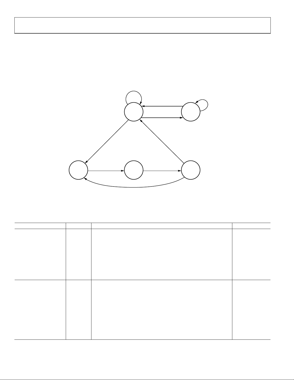
ADP1047/ADP1048 Data Sheet
STANDARD PMBus FLAGS
When the corresponding bit of a standard PMBus flag is
set in the STATUS_WORD or STATUS_BYTE register,
the programmed action takes place as shown in Figure 25.
D
T
U
H
N
S
O
C
=
0
=
1
1
0
SHUT
DOWN
RESPONSE (BITS[7:6])
RETRY SETTING (BITS[5:3])
DELAY TIME (BITS[2:0])
R
T
E
R
T
N
E
E
R
H
N
T
E
N
H
T
W
O
E
RETRY SETTING (BITS[5:3])
U
N
I
000 = NO RETRIES (OFF)
T
001 TO 110 = TRY 1 TO 6 TIMES
111 = RETRY FOREVER
NOTHING
NORMAL
OPERATION
Y
Y
R
DELAY
(BITS[2:0])
00 =
DO
TIME
Figure 25 shows the bits in the six standard PMBus fault
response registers: Register 0x41, Register 0x45, Register 0x50,
Register 0x56, Register 0x5A, and Register 0x5C. All six PMBus
fault response registers follow the same format. For more information, see the PMBus Fault Flag Response section.
FAULT CL EARED
11 = DISABLE OUT PUT
OUTPUT
DISABLED
FLAGS ARE
IGNORED
IF BLANKED
SOFT
START
FAULT
NOT
CLEARED
IF FL AG STI LL ACTI VE
01 = SHUT DO WN (AFT ER DEBOUNCE)
10 = IMMEDIATE S HUTDOWN
09696-023
Figure 25. Standard PMBus Fault Response
Table 12. Summary of Standard PMBus Flags Implemented on the ADP1047/ADP1048
Name Address Description Action
STATUS_BYTE (0x78)
PSON_OFF 0x78[6]
Power supply on signal: this flag indicates that the PSON signal (hardware
or software) is inactive.
VOUT_OV 0x78[5]
General output overvoltage fault. This flag is a combination (OR) of any output
Programmable
overvoltage flag: Register 0x7A[7] and Register 0xFE80[4] (FAST_OVP).
VIN_UV 0x78[3] General input undervoltage fault (same data as in Register 0x7C[4]). Programmable
TEMPERATURE 0x78[2] Temperature fault or warning. Programmable
CML 0x78[1] Communications, memory, or logic fault.
NONE_OF_THE_ABOVE 0x78[0] A fault or warning not listed in Register 0x78[7:1].
STATUS_WORD (0x79)
VOUT 0x79[15]
Any fault or warning on the output voltage (overvoltage, undervoltage, fast
OVP, or accurate OVP).
INPUT 0x79[13]
Input voltage, input current, or input power fault or warning (same data as
in Register 0x7C, Bits[7:0]).
MFR 0x79[12]
Manufacturer-specific fault or warning (same data as in Register 0xFE80,
Register 0xFE81, and Register 0xFE82).
POWER_GOOD# 0x79[11]
Power good. This flag is a programmable combination of other internal flags
PGOOD pin
and refers to the condition of the output voltage. This flag sets the PGOOD
pin. The POWER_GOOD# flag is an inverted version of the PGOOD pin.
UNKNOWN 0x79[8] A fault or warning not listed in Bits[15:1].
Rev. 0 | Page 26 of 84
 Loading...