Digital Power Factor Correction Controller
Preliminary Technical Data
FEATURES
Flexible, single phase, digital power factor correction (PFC)
controller
True rms ac power metering
Enhanced dynamic response
Optimized light load efficiency performance
Output voltage adjustment
Frequency reduction
Inrush control
Switching frequency spread spectrum for improved EMI
External frequency synchronization
PMBus compliant
Programmable ac line fault detection and protection
Programmable output fault detection and protection
Extensive fault protection for high reliability systems
Frequency range from 30 kHz to 400 kHz
8 kB EEPROM
Programming via easy-to-use graphical user interface (GUI)
APPLICATIONS
AC/DC power supplies for applications including
Computing server and storage
Network and communication infrastructure
Industrial and medical
GENERAL DESCRIPTION
The ADP1047 is a digital power factor correction controller
providing accurate input power metering capability and inrush
control targeting ac/dc systems.
The digital PFC function is based on a conventional boost PFC
with multiplication of the output voltage feedback combined
with the input current and voltage to provide optimum harmonic
correction and power factor for ac/dc systems. All signals are
converted into the digital domain to provide maximum
With Accurate AC Power Metering
ADP1047
flexibility—all key parameters can be reported and adjusted via
the PMBus interface. This allows users to optimize system performance, maximize efficiency across the load range, and reduce
design time to market.
The ADP1047 provides accurate, rms measurement of input
voltage, current and power. This information can be reported
to the secondary of the power supply via the PMBus interface.
The combination of a flexible, digitally controlled PFC engine
and accurate input power metering facilitate the adoption of
intelligent power management systems capable of making decisions
to improve end user system efficiency. The device targets further
efficiency improvements through programmable frequency
reduction at light load and the capability to reduce the output
voltage at low loads.
The ADP1047 provides enhanced integrated features and
functions; the Inrush and soft start control functions provide
significant component count reduction with easy design
optimization.
The device targets high reliability, redundant power supply
applications and has extensive and robust protection circuitry:
independent overvoltage protection, overcurrent (ILIM), ground
continuity metering, and ac sensing. Internal overtemperature
is provided and external temperature can be recorded via an
external sensing device.
The internal 8 kB EEPROM stores all the programmed values
and allows standalone control without a microcontroller. All
parametric reporting and adjustments are programmed via an
easy-to-use GUI—no complex programming is required.
The ADP1047 operates from a single 3.3 V supply. The device is
available in a 24-lead QSOP package specified over ambient
temperature range −40°C to +85°C.
Rev. PrA
Information furnished by Analog Devices is believed to be accurate and reliable. However, no
responsibility is assumed by Anal og Devices for its use, nor for any infringements of patents or ot her
rights of third parties that may result from its use. Specifications subject to change without notice. No
license is granted by implication or otherwise under any patent or patent rights of Analog Devices.
Trademarks and registered trademarks are the property of their respective owners.
One Technology Way, P.O. Box 9106, Norwood, MA 02062-9106, U.S.A.
Tel: 781.329.4700 www.analog.com
Fax: 781.461.3113 ©2011 Analog Devices, Inc. All rights reserved.

ADP1047 Preliminary Technical Data
TABLE OF CONTENTS
Features.............................................................................................. 1
Applications....................................................................................... 1
General Description ......................................................................... 1
Functional Block Diagram .............................................................. 3
Specifications..................................................................................... 4
Absolute Maximum Ratings ............................................................7
ESD Caution...................................................................................7
Pin Configuration And Function Descriptions ............................8
Theory of Operation .........................................................................9
Outline Dimensions....................................................................... 10
Rev. PrA | Page 2 of 12

Preliminary Technical Data ADP1047
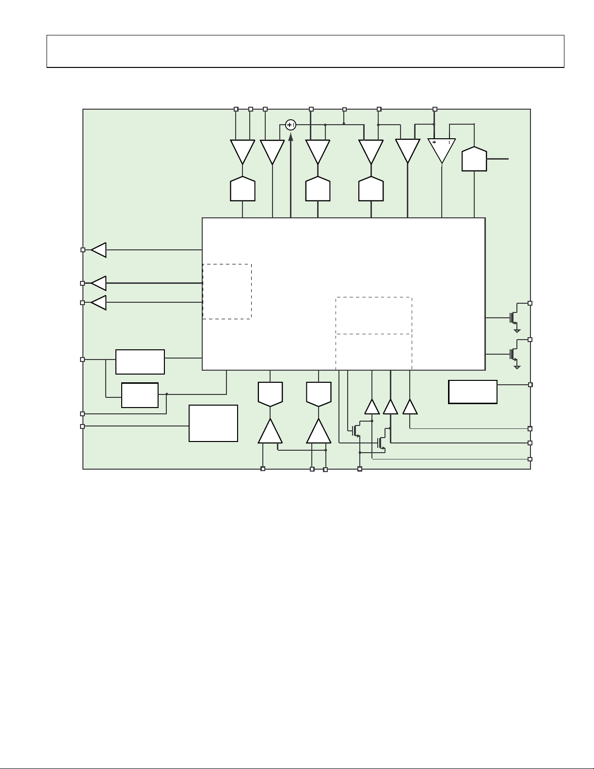
FUNCTIONAL BLOCK DIAGRAM
OVP
PGND
DAC
ADP1047
CS- CS+
ILIM
VAC PGND
VFB
INRUSH
PWM
PWM2
VDD
VCORE
RES
UVLO
LDO
PWM
ENGINE
VREF
ADC
CS
OCP
ADC
ADC
VAC
DIGITALCORE
8kb EEPROM
I2C
INTERFACE
ADC
ADC
VFB
OLP OVP
OSC
PGOOD
AC_OK
SYNC
PSON
SCL
SDA
ADD
RTD
Figure 1.
AGND
DGND
Rev. PrA | Page 3 of 12

ADP1047 Preliminary Technical Data
SPECIFICATIONS
VDD = 3.3 V TA = -40°C to +85°C, unless otherwise noted.
Table 1.
Parameter Symbol Test Conditions/Comments Min Typ Max Units
POWER SUPPLY
Operating Supply Voltage VDD 3.0 3.3 3.6 V
Supply Current IDD Normal operation (PSON high) 17 mA
Peak Supply Current I
POWER-ON RESET
POWER ON RESET VDD rising 1.8 2.95 V
UVLO VDD falling 2.80 2.85 2.90 V
OVLO 3.7 3.9 4.1 V
VAC PIN LEAKAGE CURRENT μA
OVLO Debouncing (VDD and V
) Programmable 2 500 μs
CORE
VCORE
Output Voltage Temperature = 25°C 2.3 2.5 2.7 V
PWM OUTPUT
Output Voltage
Low V
High V
Rise Time C
Fall Time C
DUTY CYCLE
Minimum Off Time Programmable 40 1200 ns
Minimum On Time Programmable 0 1200 ns
VOLTAGE SENSE INPUT RANGE
VAC
Input Voltage 0 1.6 V
VFB
Input Voltage 0 1.6 V
RTD
Input Voltage 0 1.6 V
SWITCHING FREQUENCY
Frequency Range Programmable (see Table TBD) 30 400 kHz
Accuracy −3% +3%
OSCILLATOR, CLOCK AND PLL
Oscillator Frequency 1.51 1.56 1.61 MHz
Digital Clock Frequency 200 MHz
PLL Frequency 200 MHz
RES
Output Voltage Temperature = 25°C – RES = 50 kΩ 0.98 1.0 1.02 V
Temperature Stability 320 ppm/°C
CURRENT SENSE ADC
Input Voltage Range Low Line Programmable 750 mV
Input Voltage Range High Line Programmable 500 mV
Current Source High Line 10 kΩ level shift resistor, V
Current Source Low Line 10 kΩ level shift resistor, V
Current Source Accuracy ±0.03 %
PWM
Output Low Level 0.8 V
Output High Level 2.0 V
During EEPROM programming (10 ms) 27 37 mA
DD_PK
Sink current = 10 mA 0.4 V
PWMOL
Source current = 10 mA
PWMOH
= 50 pF 3.5 ns
LOAD
= 50 pF 1.5 ns
LOAD
CS+
CS+
VDD − 0.4 V
− V
= 0 V 75 μA
CS−
− V
= 0 V 62.5 μA
CS−
V
Rev. PrA | Page 4 of 12
 Loading...