

Digital Controller for Isolated
T
Data Sheet
FEATURES
Integrates all typical PWM controller functions
7 PWM control signals
Digital control loop
Integrated programmable loop filters
Programmable voltage line feedforward
Dedicated soft start filter
Programmable dead time for improved efficiency
Remote and local voltage sense
Primary and secondary side current sense
Synchronous rectifier control
Current sharing
OrFET control
2
I
C interface
Extensive fault detection and protection
Extensive programming and telemetry
Fast digital calibration
User accessible EEPROM
APPLICATIONS
AC-to-DC power supplies
Isolated dc-to-dc power supplies
Redundant power supply systems
Server, storage, network, and communications
infrastructure
DC
INPU
Power Supply Applications
GENERAL DESCRIPTION
The ADP1046 is a flexible, digital secondary side controller
designed for ac-to-dc and isolated dc-to-dc secondary side
applications. The ADP1046 is pin-compatible with the
ADP1043A and offers several enhancements and new features,
including voltage feedforward, improved loop response, and
programmable dead time control to maximize efficiency.
The ADP1046 is optimized for minimal component count,
maximum flexibility, and minimum design time. Features
include local and remote voltage sense, primary and secondary
side current sense, digital pulse-width modulation (PWM)
generation, current sharing, and redundant OrFET control. The
control loop digital filter and compensation terms are integrated
and can be programmed over the I
protection features include overcurrent protection (OCP), overvoltage protection (OVP), undervoltage lockout (UVLO), and
overtemperature protection (OTP).
The built-in EEPROM provides extensive programming of the
integrated loop filter, PWM signal timing, inrush current, and
soft start timing and sequencing. Reliability is improved through
a built-in checksum and programmable protection circuits.
A comprehensive GUI is provided for easy design of loop
filter characteristics and programming of the safety features.
The industry-standard I
monitoring and system test functions.
The ADP1046 is available in a 32-lead LFCSP and operates
from a single 3.3 V supply.
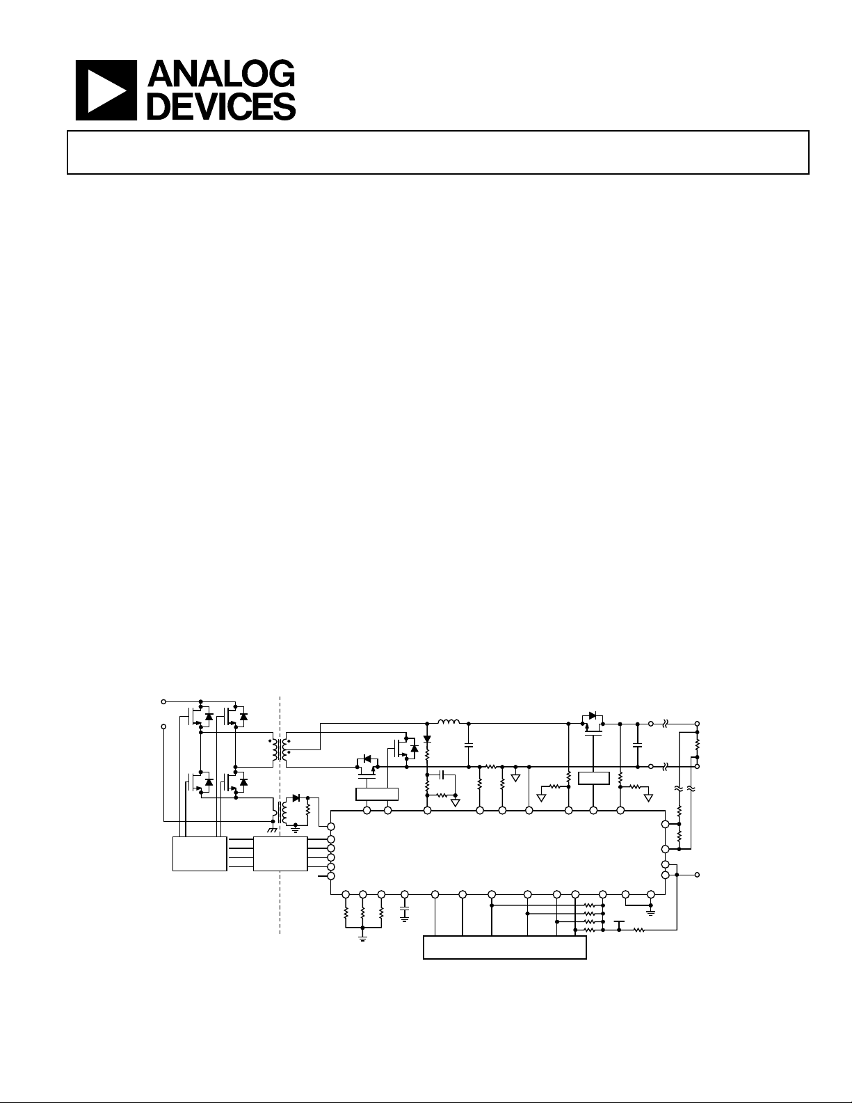
TYPICAL APPLICATION CIRCUIT
ADP1046
2
C interface. Programmable
2
C bus provides access to the many
LOAD
DRIVER
DRIVER
SR1 SR2 ACSNS VS1 GATE
CS1
OUTA
DRIVER
Rev. A
Information furnished by Analog Devices is believed to be accurate and reliable. However, no
responsibility is assumed by Analog Devices for its use, nor for any infringements of patents or other
rights of third parties that may result from its use. Specifications subject to change without notice. No
license is granted by implication or otherwise under any patent or patent rights of Analog Devices.
Trademarks and registered trademarks are the property of their respective owners.
iCoupler
OUTB
OUTC
OUTD
OUTAUX
RES RTDADD VCORE FLAGIN PSON PGOOD2 PGOOD1 SDA SCL VDD DGND AGND
Figure 1.
CS2– CS2+ PGND
ADP1046
MICROCONTROLLER
One Technology Way, P.O. Box 9106, Norwood, MA 02062-9106, U.S.A.
Tel: 781.329.4700 www.analog.com
Fax: 781.461.3113 ©2012 Analog Devices, Inc. All rights reserved.
VS2
V
DD
VS3+
VS3–
SHAREo
SHAREi
10045-001

ADP1046 Data Sheet
TABLE OF CONTENTS
Features .............................................................................................. 1
Applications ....................................................................................... 1
General Description ......................................................................... 1
Typical Application Circuit ............................................................. 1
Revision History ............................................................................... 3
Functional Block Diagram .............................................................. 4
Specifications ..................................................................................... 5
Absolute Maximum Ratings .......................................................... 10
Thermal Resistance .................................................................... 10
Soldering ...................................................................................... 10
ESD Caution ................................................................................ 10
Pin Configuration and Function Descriptions ........................... 11
Typical Performance Characteristics ........................................... 13
Theory of Operation ...................................................................... 15
Current Sense .............................................................................. 15
Voltage Sense and Control Loop .............................................. 16
ADCs ............................................................................................ 16
VS1 Operation (VS1) ................................................................. 16
VS2 Operation (VS2) ................................................................. 17
VS3 Operation (VS3+, VS3−) ................................................... 17
Voltage Line Feedforward and ACSNS.................................... 17
Digital Filter ................................................................................ 17
PWM and Sync Rect Outputs (OUTA, OUTB, OUTC,
OUTD, OUTAUX, SR1, SR2) ................................................... 18
Synchronous Rectification ........................................................ 19
SR (Synchronous Rectifier) Delay ............................................ 19
Adaptive Dead Time Control.................................................... 19
Light Load Mode ........................................................................ 19
Modulation Limit ....................................................................... 19
Soft Start ...................................................................................... 20
OrFET Control (GATE) ............................................................ 22
VDD ............................................................................................. 24
VDD/VCORE OVLO ................................................................ 24
Power Good ................................................................................. 24
Current Sharing (Share) ............................................................ 25
Power Supply System and Fault Monitoring ............................... 27
Flags .............................................................................................. 27
Monitoring Functions ................................................................ 27
Voltage Readings ........................................................................ 27
Current Readings ........................................................................ 27
Rev. A | Page 2 of 96
Power Readings .......................................................................... 28
Power Monitoring Accuracy ..................................................... 28
First Flag Fault ID and Value Registers ................................... 28
External Flag Input (FLAGIN Pin) .......................................... 28
Temperature Readings (RTD Pin) ........................................... 28
Overtemperature Protection (OTP) ........................................ 29
Overcurrent Protection (OCP) ................................................ 29
Constant Current Mode ............................................................ 30
Overvoltage Protection (OVP) ................................................. 30
Undervoltage Protection (UVP) .............................................. 31
AC Sense (ACSNS)..................................................................... 31
Volt-Second Balance .................................................................. 32
Digital Load Line and Slew Rate .............................................. 32
Power Supply Calibration and Trim ............................................ 33
CS1 Tri m ...................................................................................... 33
CS2 Tri m ...................................................................................... 33
Voltage Calibration and Trim ................................................... 34
Output Voltage Setting (VS3+, VS3− Trim) ........................... 34
VS1 Trim ...................................................................................... 34
VS2 Trim ...................................................................................... 34
RTD/OTP Trim .......................................................................... 34
ACSNS Calibration and Trim ................................................... 35
Layout Guidelines ........................................................................... 36
CS2+ and CS2− ........................................................................... 36
VS3+ and VS3−........................................................................... 36
VDD ............................................................................................. 36
SDA and SCL .............................................................................. 36
CS1 ............................................................................................... 36
Exposed Pad ................................................................................ 36
VCORE ........................................................................................ 36
RES ............................................................................................... 36
RTD .............................................................................................. 36
AGND, DGND, and PGND ...................................................... 36
I2C Interface Communication ...................................................... 37
Features ........................................................................................ 37
Overview ..................................................................................... 37
I2C Address .................................................................................. 37
Data Transfer............................................................................... 37
General Call Support ................................................................. 39
10-Bit Addressing ....................................................................... 39

Data Sheet ADP1046
Fast Mode ..................................................................................... 39
Repeated Start Condition ........................................................... 39
Electrical Specifications .............................................................. 39
Fault Conditions .......................................................................... 39
Timeout Condition ..................................................................... 39
Data Transmission Faults ........................................................... 39
Data Content Faults .................................................................... 39
EEPROM .......................................................................................... 41
Overview ...................................................................................... 41
Page Erase Operation ................................................................. 41
Read Operation (Byte Read and Block Read) ......................... 41
Write Operation (Byte Write and Block Write) ...................... 42
EEPROM Password..................................................................... 42
Downloading EEPROM Settings to Internal Registers .......... 42
Saving Register Settings to the EEPROM ................................ 43
EEPROM CRC Checksum ......................................................... 43
Software GUI ................................................................................... 44
Register Listing ................................................................................ 45
Detailed Register Descriptions ...................................................... 49
Fault Registers .............................................................................. 49
Value Registers ............................................................................. 52
Current Sense and Current Limit Registers ............................ 55
Voltage Sense Registers............................................................... 60
REVISION HISTORY
6/12—Rev. 0 to Rev. A
Changes to Table 1 ............................................................................ 6
Change to Table 2 ............................................................................ 10
Change to Read from Main Block, Page 2 to Page 15 Section .. 41
Change to Write to Main Block, Page 4 to Page 15 Section ...... 42
Change to Table 49 .......................................................................... 60
3/12—Revision 0: Initial Version
ID Registers .................................................................................. 63
PWM and Synchronous Rectifier Timing Registers .............. 64
Digital Filter Programming Registers ...................................... 74
Adaptive Dead Time Registers .................................................. 76
Soft Start Filter Programming Registers .................................. 80
Extended Functions Registers ................................................... 81
EEPROM Registers ..................................................................... 84
Resonant Mode Operation ............................................................. 87
Resonant Mode Enable ............................................................... 87
PWM Timing in Resonant Mode ............................................. 87
Synchronous Rectification in Resonant Mode ........................ 87
Adjusting the Timing of the PWM Outputs ........................... 88
Frequency Limit Setting ............................................................. 88
Feedback Control in Resonant Mode ....................................... 88
Soft Start in Resonant Mode ...................................................... 88
Light Load Operation (Burst Mode) ........................................ 88
OUTAUX in Resonant Mode .................................................... 88
Protections in Resonant Mode .................................................. 88
Resonant Mode Register Descriptions ..................................... 89
Outline Dimensions ........................................................................ 93
Ordering Guide ........................................................................... 93
Rev. A | Page 3 of 96
ADP1046 Data Sheet
RES
VS3–
VS3+
PGOOD1
VDD
GATE
PGND
ACSNS
VS1
OUTA
OUTB
SR1
SR2
OUTC
OUTD
CS1
PSON
SCL
SDA
CS2–
CS2+
VS2
VCORE
AGND
OUTAUX
PGOOD2
SHAREi
FLAGIN
DGND
RTDADD
ADC
ADC ADC
ADC
ADC
UVLO
PWM
ENGINE
V
REF
LDO
ADC
ADC
8kB
EEPROM
DIGITAL
CORE
I
2
C
INTERFACE
PWM
OSC
1.2V
+ –
0.45V
+ –
V_OVP
SHAREo
10045-002
ADP1046
The ADP1046 is a secondary side controller for switch mode
power supplies (SMPS). It is designed for use in isolated redundant applications. The ADP1046 integrates the typical functions
that are needed to control a power supply, such as
• Output voltage sense and feedback
• Voltage line feedforward control
• Digital loop filter compensation
• PWM generation
• Current sharing
• Current, voltage, and temperature sense
• OrFET control
• Housekeeping and I
2
C interface
• Calibration and trimming
The main function of controlling the output voltage is performed
using the feedback ADCs, the digital loop filter, and the PWM
block.
The feedback ADCs use a multipath approach (patent pending).
The ADP1046 combines a high speed, low resolution (fast and
coarse) ADC with a low speed, high resolution (slow and accurate)
ADC. Loop compensation is implemented using the digital filter.
This proportional, integral, derivative (PID) filter is implemented
in the digital domain to allow easy programming of filter characteristics, which is of great value in customizing and debugging
designs.
FUNCTIONAL BLOCK DIAGRAM
The PWM block generates up to seven programmable PWM
outputs for control of FET drivers and synchronous rectification
FET drivers. This programmability allows many traditional and
unique switching topologies to be realized.
A current share bus interface is provided for paralleling multiple
power supplies. The ADP1046 also has hot-swap OrFET sense
and control for N + 1 redundant power supplies.
Conventional power supply housekeeping features, such as remote
and local voltage sense and primary and secondary side current
sense, are included. An extensive set of protections is offered,
including overvoltage protection (OVP), overcurrent protection
(OCP), overtemperature protection (OTP), undervoltage protection (UVP), ground continuity monitoring (voltage continuity),
and ac sense.
All these features are programmable through the I
2
C bus interface. This bus interface is also used to calibrate the power supply.
Other information that is useful for power monitoring, such as
input current, output current, and fault flags, is also available
through the I
2
C bus interface.
The internal EEPROM can store all programmed values and
allows standalone control without a microcontroller. A free,
downloadable GUI is available and provides all the necessary
software to program the ADP1046. To obtain the latest software
and a user guide, visit http://www.analog.com/digitalpower.
The ADP1046 operates from a single 3.3 V supply and is specified
from −40°C to +125°C.
Figure 2. ADP1046 Simplified Block Diagram
Rev. A | Page 4 of 96

Data Sheet ADP1046
OVLO
3.8
4.0
4.1
V
LOAD
LOAD
−48 +48
mV
Temperature Coefficient
65
ppm/°C
Leakage Current
1.0
µA
resolution is 7 bits
VS2 and VS3 OVP Threshold
Relative to nominal voltage (1 V) on VS2
−2.0 +2.0
% FSR
SPECIFICATIONS
VDD = 3.0 V to 3.6 V, TA = −40°C to +125°C, unless otherwise noted. FSR = full-scale range.
Table 1.
Parameter Symbol Test Conditions/Comments Min Typ Max Unit
SUPPLY
Supply Voltage VDD 4.7 µF capacitor connected to AGND 3.0 3.3 3.6 V
Supply Current IDD Normal operation (PSON is high or low) 20 mA
During EEPROM programming (40 ms) IDD + 8 mA
Shutdown (VDD below UVLO) 100 µA
POWER-ON RESET
Power-On Reset VDD rising 3.0 V
UVLO VDD falling 2.75 2.85 2.97 V
UVLO Hysteresis 40 mV
OVLO Debounce When set to 2 µs 2.0 µs
When set to 500 µs 500 µs
VCORE PIN 0.33 µF capacitor connected to DGND
Output Voltage TA = 25°C 2.4 2.5 2.7 V
OSCILLATOR AND PLL
PLL Frequency RES = 10 kΩ (±0.1%) 190 200 210 MHz
OUTA, OUTB, OUTC, OUTD,
OUTAUX, SR1, SR2, GATE PINS
Output Low Voltage VOL Source current = 10 mA 0.4 V
Output High Voltage VOH Source current = 10 mA VDD − 0.4 V
Rise Time C
Fall Time C
VS1, VS2, VS3 LOW SPEED ADCs
Input Voltage Range VIN Differential voltage from VS1, VS2 to
Usable Input Voltage Range 0 1.4 V
ADC Clock Frequency 1.56 MHz
Register Update Rate 10 ms
Voltage Sense Measurement
Accuracy
0% to 100% of usable input voltage range −3.0 +3.0 % FSR
= 50 pF 3.5 ns
= 50 pF 1.5 ns
0 1 1.6 V
PGND, and from VS3+ to VS3−
Factory trimmed at 1.0 V
10% to 90% of usable input voltage range −2.0 +2.0 % FSR
−32 +32 mV
900 mV to 1.1 V −1.0 +1.0 % FSR
−16 +16 mV
Voltage Sense Measurement
Resolution
Common-Mode Voltage Offset −0.25 +0.25 % FSR
Voltage Differential from VS3−
to PGND
VS1 Accurate OVP Speed Register 0x32[1:0] = 00; equivalent
VS1 OVP Threshold Accuracy Relative to nominal voltage (1 V) on VS1 −2.0 +2.0 % FSR
VS2 and VS3 OVP Speed Register 0x33[1:0] = 00; equivalent
Accuracy
12 Bits
−200 +200 mV
80 µs
resolution is 7 bits
80 µs
and VS3
Rev. A | Page 5 of 96

ADP1046 Data Sheet
At other thresholds (0.8 V to 1.6 V)
−2.06
+2.06
%
ADC Clock Frequency
1.56 MHz
ACSNS
Input Voltage Range
VIN 0 1 1.4
V
Parameter Symbol Test Conditions/Comments Min Typ Max Unit
VS3 HIGH SPEED ADC
Equivalent Sampling
Frequency
Equivalent Resolution fSW = 390.6 kHz 6 Bits
Dynamic Range ±30 mV
VS1 FAST OVP COMPARATOR
Threshold Accuracy At factory trim of 1.2 V 1 1.60 %
f
fSW kHz
SAMP
Propagation Delay Does not include debounce time
40 ns
(Register 0x0A[7] = 1)
VS1 UVP DIGITAL COMPARATOR
VS1 UVP Accuracy −2.0 +2.0 % FSR
Propagation Delay Does not include debounce time
80 µs
(Register 0x0B[3] = 1)
AC SENSE COMPARATOR PWM and resonant mode
Input Voltage Threshold 0.4 0.45 0.5 V
Propagation Delay
From ACSNS threshold to SRx rising edge
160 ns
(resonant mode only)
Input Voltage Range V
0 1 1.6 V
Usable Input Voltage Range 0 1.4 V
Sampling Frequency for I2C
100 Hz
Reporting
Sampling Period for
Equivalent resolution is 11 bits 10 µs
Feedforward
Measurement Accuracy Factory trimmed at 1.0 V
0% to 100% of usable input voltage range −5.0 +3.0 % FSR
10% to 90% of usable input voltage range −2.0 +2.0 % FSR
900 mV to 1.1 V −1.0 +1.0 % FSR
−16 +16 mV
Leakage Current 1.0 µA
CURRENT SENSE 1 (CS1 PIN)
Usable Input Voltage Range 0 1.3 V
ADC Clock Frequency 1.56 MHz
Register Update Rate 10 ms
Current Sense Measurement
Accuracy
Factory trimmed at 0.7 V; tested under dc
input conditions
10% to 50% of usable input voltage range −3.0 +3.0 % FSR
−41.4 +41.4 mV
0% to 100% of usable input voltage range −6.0 +3.0 % FSR
−84 +42 mV
40% to 60% of usable input voltage range −1.0 +1.0 % FSR
Current Sense Measurement
12 Bits
Resolution
CS1 Fast OCP Threshold 1.184 1.2 1.216 V
CS1 Fast OCP Speed 80 100 ns
CS1 Accurate OCP DC Accuracy 10% to 90% of usable input voltage range −2.0 +2.0 % FSR
−28 +28 mV
CS1 Accurate OCP Speed 2.62 5.24 ms
Leakage Current 1.0 μA
Rev. A | Page 6 of 96

Data Sheet ADP1046
Usable Input Voltage Range
0 110
mV
60 mV Setting
0 mV to 55 mV, VDD = 3.3 V
−1.8 +1.8
% FSR
−2.16
+2.16
mV
−18 mV setting
−12.22
−19.07
−25.92
mV
Current source set to 40 µA
38.45
40.3
41.95
µA
Parameter Symbol Test Conditions/Comments Min Typ Max Unit
CURRENT SENSE 2 (CS2+, CS2−
PINS)
Input Voltage Range VIN Differential voltage from CS2+ to CS2−,
ADC Clock Frequency 1.56 MHz
Temperature Coefficient
120 mV Range 0 mV to 100 mV 78 ppm/°C
0 mV to 50 mV 70 ppm/°C
60 mV Range 0 mV to 50 mV 156 ppm/°C
0 mV to 25 mV 140 ppm/°C
Current Sense Measurement
120 mV Setting 0 mV to 110 mV −2.1 +2.1 % FSR
−2.52 +2.52 mV
60 mV Setting 0 mV to 55 mV −4.2 +4.2 % FSR
−5.04 +5.04 mV
Current Sense Measurement
Accuracy
120 mV Setting 0 mV to 100 mV, VDD = 3.3 V −0.9 +0.9 % FSR
−1.08 +1.08 mV
0 120 mV
LSB = 29.297 μV
With 0.01% level shifting resistors
Current Sense Measurement
Resolution
CS2 Accurate OCP Speed 2.62 5.24 ms
Current Sink (High Side) 2 mA
Current Source (Low Side) 200 μA
Common-Mode Voltage at the
CS2+ and CS2− Pins
OrFET PROTECTION (CS2+, CS2−) Low-side and high-side current sensing
Fast OrFET Accuracy −3 mV setting +3.5 −3.00 −9.5 mV
−6 mV setting +0.29 −6.21 −12.71 mV
−9 mV setting −2.68 −9.43 −16.18 mV
−12 mV setting −5.89 −12.64 −19.39 mV
−15 mV setting −9.01 −15.86 −22.71 mV
−21 mV setting −15.29 −22.29 −29.29 mV
−24 mV setting −18.50 −25.50 −32.50 mV
Fast OrFET Speed Debounce = 40 ns 110 150 ns
RTD TEMPERATURE SENSE
ADC Clock Frequency 1.56 MHz
Input Voltage Range RTD to AGND 0 1.6 V
Usable Input Voltage Range 0 1.3 V
Source Current Factory trimmed to 46 μA (Register 0x11
Current source set to 10 µA 9.25 10.1 10.85 µA
Current source set to 20 µA 18.35 20.1 21.85 µA
Current source set to 30 µA 28.45 30.2 31.95 µA
12 Bits
To achieve CS2 measurement accuracy 0.8 1.0 1.4 V
44.35 46 47.65 µA
set to 0xE6)
Source Current Fine Setting See Register 0x11[5:0] 160 nA
RTD ADC
Register Update Rate 10 ms
Resolution 12 Bits
Rev. A | Page 7 of 96

ADP1046 Data Sheet
−42 +42
mV
EXT
SDA/SCL PINS
VDD = 3.3 V
BUF
SU;STA
SU;STO
SU ;D AT
SDA Hold Time
t
HD;DAT
For readback
125
ns
For write
300
ns
TIMEOUT
LOW
HIGH
LO;SEXT
Parameter Symbol Test Conditions/Comments Min Typ Max Unit
Measurement Accuracy Factory trimmed at 1 V
10 mV to 160 mV −0.5 +0.5 % FSR
−8 +8 mV
0% to 100% of usable input voltage range −3.0 +3.0 % FSR
Temperature Readings
According to Internal
Linearization Scheme
RTD source set to 46 µA (Register 0x11 set to
0xE6); NTC R0 = 100 kΩ, 1%, beta = 4250, 1%;
R
= 16.5 kΩ, 1%
25°C to 100°C 7 °C
100°C to 125°C 5 °C
OTP
Threshold Accuracy T = 85°C with 100 kΩ||16.5 kΩ −0.9 +0.25 % FSR
−14.4 +4 mV
T = 100°C with 100 kΩ||16.5 kΩ −0.5 +1.1 % FSR
−8 +17.6 mV
Comparator Speed 10.5 ms
OTP Threshold Hysteresis 16 mV
PGOOD1, PGOOD2, SHAREo PINS Open-drain outputs
Output Low Voltage VOL 0.4 V
PSON, SHAREi PINS Digital inputs
Input Low Voltage VIL 0.8 V
Input High Voltage VIH VDD − 0.8 V
Leakage Current 1.0 µA
FLAGIN PIN Digital input
Input Low Voltage VIL 0.4 V
Input High Voltage VIH VDD − 0.8 V
Propagation Delay Does not include debounce time (Register
200 ns
0x0A[3] = 1); flag action set to disable PSU
Leakage Current 1.0 µA
GATE PIN
Output Low Voltage VOL 0.4 V
Output High Voltage VOH VDD − 0.4 V
Input Low Voltage VIL 0.8 V
Input High Voltage VIH VDD − 0.8 V
Output Low Voltage VOL 0.4 V
Leakage Current 1.0 µA
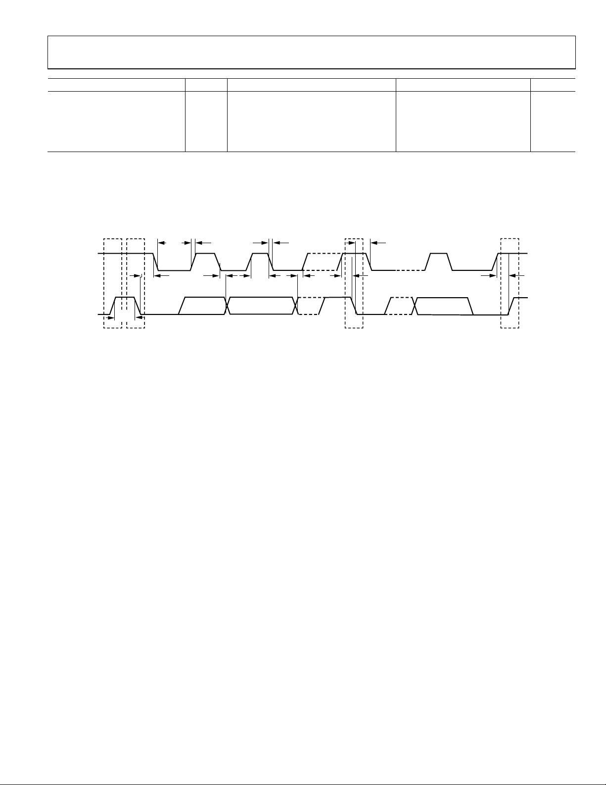
SERIAL BUS TIMING See Figure 3
Clock Operating Frequency 10 100 400 kHz
Bus-Free Time t
Start Hold Time t
Start Setup Time t
Stop Setup Time t
SDA Setup Time t
SCL Low Timeout t
SCL Low Period t
SCL High Period t
Clock Low Extend Time t
SCL, SDA Fall Time tF 20 300 ns
SCL, SDA Rise Time tR 20 300 ns
Between stop and start conditions 1.3 µs
HD;STA
Hold time after (repeated) start condition;
0.6 µs
after this period, the first clock is generated
Repeated start condition setup time 0.6 µs
0.6 µs
100 ns
25 35 ms
1.3 µs
0.6 µs
25 ms
Rev. A | Page 8 of 96
Data Sheet ADP1046
TJ = 125°C
10
Years
SCL
SDA
P S
t
BUF
t
HD;STA
t
HD;DAT
t
HIGH
t
SU;DAT
t
HD;STA
t
SU;STA
t
SU;STO
t
LOW
t
R
t
F
S P
10045-103
Parameter Symbol Test Conditions/Comments Min Typ Max Unit
EEPROM RELIABILITY
Endurance1 TJ = 85°C 10,000 Cycles
TJ = 125°C 1000 Cycles
Data Retention2 TJ = 85°C 20 Years
1
Endurance is qualified as per JEDEC Standard 22, Method A117, and is measured at −40°C, +25°C, +85°C, and +125°C. Endurance conditions are subject to change
pending EEPROM qualification.
2
Retention lifetime equivalent at junction temperature (TJ) = 85°C as per JEDEC Standard 22, Method A117. The derated retention lifetime equivalent at junction
temperature T
Timing Diagram
= 125°C is 2.87 years and is subject to change pending EEPROM qualification.
J
Figure 3. Serial Bus Timing Diagram
Rev. A | Page 9 of 96
ADP1046 Data Sheet
Digital Pins: OUTA, OUTB, OUTC, OUTD,
−0.3 V to VDD + 0.3 V
RTD, ADD
−0.3 V to VDD + 0.3 V
(20 sec to 40 sec)
ESD Charged Device Model
1.5 kV
ABSOLUTE MAXIMUM RATINGS
Table 2.
Parameter Rating
Supply Voltage (Continuous), VDD 4.2 V
THERMAL RESISTANCE
θJA is specified for the worst-case conditions, that is, a device
soldered in a circuit board for surface-mount packages.
OUTAUX, SR1, SR2, GATE, PGOOD1,
PGOOD2
VS3− to PGND, AGND, DGND −0.3 V to +0.3 V
VS1, VS2, VS3+, ACSNS −0.3 V to VDD + 0.3 V
CS1, CS2+, CS2− −0.3 V to VDD + 0.3 V
FLAGIN, PSON −0.3 V to VDD + 0.3 V
SDA, SCL −0.3 V to VDD + 0.3 V
SHAREo, SHAREi −0.3 V to VDD + 0.3 V
Operating Temperature Range −40°C to +125°C
Storage Temperature Range −65°C to +150°C
Junction Temperature 150°C
Peak Solder Reflow Temperature
SnPb Assemblies (10 sec to 30 sec) 240°C
RoHS-Compliant Assemblies
ESD Human Body Model 3.5 kV
260°C
Stresses above those listed under Absolute Maximum Ratings
may cause permanent damage to the device. This is a stress
rating only; functional operation of the device at these or any
other conditions above those indicated in the operational
section of this specification is not implied. Exposure to absolute
maximum rating conditions for extended periods may affect
device reliability.
Table 3. Thermal Resistance
Package Type θJA θJC Unit
32-Lead LFCSP 44.4 6.4 °C/W
SOLDERING
It is important to follow the correct guidelines when laying out
the PCB footprint for the ADP1046 and when soldering the
part onto the PCB. For detailed information about these guidelines, see the AN-772 Application Note.
ESD CAUTION
Rev. A | Page 10 of 96

Data Sheet ADP1046
PIN 1
INDICATOR
1VS2
2AGND
3VS1
4CS2–
5CS2+
6ACSNS
7CS1
8PGND
24 SHAREi
23 SHAREo
22 PGOOD1
21 PGOOD2
20 FLAGIN
19 PSON
18 SDA
17 SCL
9SR1
10SR2
11OUTA
12OUTB
13OUTC
14OUTD
15OUTAUX
16GATE
32
VS3+
31
VS3–
30
RES
29
ADD
28
RTD
27
VDD
26
VCORE
25
DGND
ADP1046
TOP VIEW
(Not to S cale)
NOTES
1. THE ADP1046 HAS AN EXPOSED THERMAL PAD ON THE UNDERSIDE
OF THEPACKAGE. FOR INCREASED RELIABILITY OF THE SOLDER
JOINTSAND MAXIM UM THERMAL CAPABILITY, IT IS RECOMMENDED
THAT THE PAD BE SOLDERED TO THE PCB AGND PLANE.
10045-003
4
CS2−
Inverting Differential Current Sense Input. Nominal voltage at this pin should be 1 V for best operation. When
9
SR1
Synchronous Rectifier Output. This PWM output connects to the input of a FET driver. This pin can be disabled
PIN CONFIGURATION AND FUNCTION DESCRIPTIONS
Figure 4. Pin Configuration
Table 4. Pin Function Descriptions
Pin No. Mnemonic Description
1 VS2 Power Supply Output Voltage Sense Input. This signal is referenced to PGND and is the input to a low frequency
Σ-Δ ADC. Nominal voltage at this pin should be 1 V. The resistor divider on this input must have a tolerance
specification of 0.5% or better to allow for trimming.
2 AGND Analog Ground. This pin is the ground for the analog circuitry and the return for the VDD pin of the ADP1046.
3 VS1 Local Output Voltage Sense Input. This signal is referenced to PGND. Nominal voltage at this pin should be 1 V.
The resistor divider on this input must have a tolerance specification of 0.5% or better to allow for trimming.
using low-side current sensing, place a 5 kΩ resistor between the sense resistor and this pin. When using high-
side current sensing in a 12 V application, place a 5.5 kΩ resistor between the sense resistor and this pin. When
using high-side current sensing with a voltage other than 12 V, use this formula to calculate the resistor value:
R = (V
− 1)/2 mA. A 0.1% resistor must be used to connect this circuit. If this pin is not used, connect it to PGND
OUT
and set CS2± to high-side current sense mode (set Bit 2 of Register 0x27). It is recommended that a 500 pF to
1000 pF capacitor be connected either across the resistor or from this pin to AGND.
5 CS2+ Noninverting Differential Current Sense Input. Nominal voltage at this pin should be 1 V for best operation.
When using low-side current sensing, place a 5 kΩ resistor between the sense resistor and this pin. When using
high-side current sensing in a 12 V application, place a 5.5 kΩ resistor between the sense resistor and this pin.
When using high-side current sensing with a voltage other than 12 V, use this formula to calculate the resistor
value: R = (V
− 1)/2 mA. A 0.1% resistor must be used to connect this circuit. If this pin is not used, connect it
OUT
to PGND and set CS2± to high-side current sense mode (set Bit 2 of Register 0x27). It is recommended that a
500 pF to 1000 pF capacitor be connected either across the resistor or from this pin to AGND.
6 ACSNS AC Sense Input. This input is connected upstream of the main output inductor through a resistor divider
network. The nominal voltage for this circuit is 0.45 V. This pin is also connected to the voltage feedforward
ADC (nominal voltage 1 V). This signal is referenced to PGND.
7 CS1 Primary Side Current Sense Input. This pin is connected to the primary side current sensing ADC and to the fast
OCP comparator. This signal is referenced to PGND. The resistors on this input must have a tolerance specification
8 PGND Power Ground. This pin is the ground connection for the main power rail of the power supply and is the
10 SR2 Synchronous Rectifier Output. This PWM output connects to the input of a FET driver. This pin can be disabled
11 OU TA PWM Output for Primary Side Switch. This pin can be disabled when not in use. This signal is referenced to AGND.
12 OUTB PWM Output for Primary Side Switch. This pin can be disabled when not in use. This signal is referenced to AGND.
of 0.5% or better to allow for trimming. If this pin is not used, connect it to PGND.
reference for all voltage and current sensing other than CS2± and VS3±. Star connect to AGND.
when not in use. This signal is referenced to AGND.
when not in use. This signal is referenced to AGND.
Rev. A | Page 11 of 96

ADP1046 Data Sheet
17
SCL
I2C Serial Clock Input. This signal is referenced to AGND.
this pin is 1 V. The resistor divider on this input must have a tolerance specification of 0.5% or better to allow for
Pin No. Mnemonic Description
13 OUTC PWM Output for Primary Side Switch. This pin can be disabled when not in use. This signal is referenced to AGND.
14 OUTD PWM Output for Primary Side Switch. This pin can be disabled when not in use. This signal is referenced to AGND.
15 OUTAUX Auxiliary PWM Output. This pin can be disabled when not in use. This signal is referenced to AGND.
16 GATE OrFET Gate Drive Output. This signal is referenced to AGND. If this pin is not used, leave it floating.
18 SDA I2C Serial Data Input and Output (Open Drain). This signal is referenced to AGND.
19 PSON Power Supply On Input. This signal is referenced to AGND. This pin is the hardware PSON control signal. It is
recommended that a 1 nF capacitor be connected from the PSON pin to AGND for noise debouncing and
decoupling.
20 FLAGIN Flag Input. An external signal can be input at this pin to generate a flag condition.
21 PGOOD2 Power-Good Output (Open Drain). This signal is referenced to AGND. This pin is controlled by the PGOOD2 flag.
This pin is set by a programmable combination of internal flags. If this pin is not used, connect it to AGND.
22 PGOOD1 Power-Good Output (Open Drain). This signal is referenced to AGND. This pin is controlled by the PGOOD1 flag.
This pin is set by a programmable combination of internal flags. If this pin is not used, connect it to AGND.
23 SHAREo Share Bus Output Voltage Pin. Connect this pin to 3.3 V through a pull-up resistor (typically 2.2 kΩ). When
configured for a digital share bus, this pin is a digital output. This signal is referenced to AGND. If this pin is
not used, connect it to AGND.
24 SHAREi Share Bus Feedback Pin. Connect this pin to the SHAREo pin. This signal is referenced to AGND. If this pin is not
used, connect it to AGND.
25 DGND Digital Ground. This pin is the ground reference for the digital circuitry of the ADP1046. Star connect to AGND.
26 VCORE Output of the 2.5 V Regulator. Connect a decoupling capacitor of at least 330 nF (1 µF maximum) from this pin
to DGND as close to the IC as possible to minimize PCB trace length. It is recommended that the VCORE pin not
be used as a reference or to generate other logic levels using resistive dividers.
27 VDD Positive Supply Input. This signal is referenced to AGND. Connect a 4.7 µF decoupling capacitor from this pin to
AGND as close to the IC as possible to minimize PCB trace length.
28 RTD Thermistor Input. Place a thermistor (100 kΩ, 1%, beta = 4250, 1%) in parallel with a 16.5 kΩ, 1% resistor. This
pin is referenced to AGND. If this pin is not used, connect it to AGND.
29 ADD Address Select Input. This pin is used to program the I2C address. Connect a resistor from ADD to AGND. This
signal is referenced to AGND.
30 RES Resistor Input. This pin sets up the internal voltage reference for the ADP1046. Connect a 10 kΩ, ±0.1% resistor
from RES to AGND. This signal is referenced to AGND.
31 VS3− Inverting Remote Voltage Sense Input. There should be a low ohmic connection to AGND. The resistor divider
on this input must have a tolerance specification of 0.5% or better to allow for trimming. Connect a 0.1 µF
capacitor from VS3− to AGND.
32 VS3+ Noninverting Remote Voltage Sense Input. This signal is referenced to VS3−, and the nominal input voltage at
trimming. This pin is the input to the high frequency Δ-Σ ADC.
EP Exposed Pad. The ADP1046 has an exposed thermal pad on the underside of the package. For increased
reliability of the solder joints and maximum thermal capability, it is recommended that the pad be soldered
to the PCB AGND plane.
Rev. A | Page 12 of 96
Data Sheet ADP1046
2.5
–2.5
–2.0
–1.5
–1.0
–0.5
0
0.5
1.0
1.5
2.0
–60 –40 –20 0 20 40 60 80 100 120 140
VS1 ADC ACCURACY (%FSR)
TEMPERATURE (°C)
10045-400
MAX SPEC
MIN SPEC
MIN MEAN
MAX
2.5
–2.5
–2.0
–1.5
–1.0
–0.5
0
0.5
1.0
1.5
2.0
–60 –40 –20 0 20 40 60 80 100 120 140
VS2 ADC ACCURACY (%FSR)
TEMPERATURE (°C)
10045-401
MAX SPEC
MIN SPEC
MIN MEAN
MAX
2.5
–2.5
–2.0
–1.5
–1.0
–0.5
0
0.5
1.0
1.5
2.0
–60 –40 –20 0 20 40 60 80 100 120 140
VS3 ADC ACCURACY (%FSR)
TEMPERATURE (°C)
10045-402
MAX SPEC
MIN SPEC
MIN MEAN
MAX
2.5
–2.5
–2.0
–1.5
–1.0
–0.5
0
1.0
0.5
1.5
2.0
–60 –40 –20 0 20 40 60 80 100 120 140
CS1 ADC ACCURACY (%FSR)
TEMPERATURE (°C)
10045-403
MAX SPEC
MIN SPEC
MIN
MEAN
MAX
2.5
–2.5
–2.0
–1.5
–1.0
–0.5
0
1.0
0.5
1.5
2.0
–60 –40 –20 0 20 40 60 80 100 120 140
CS2 ADC ACCURACY (%FSR)
TEMPERATURE (°C)
10045-404
MAX SPEC
MIN SPEC
MIN
MEAN
MAX
1.24
1.16
1.17
1.18
1.19
1.20
1.21
1.22
1.23
–60 –40 –20 0 20 40 60 80 100 120 140
CS1 FAST O CP THRESHOLD (V )
TEMPERATURE (°C)
10045-405
MIN
MAX
MAX SPEC
MIN SPEC
MEAN
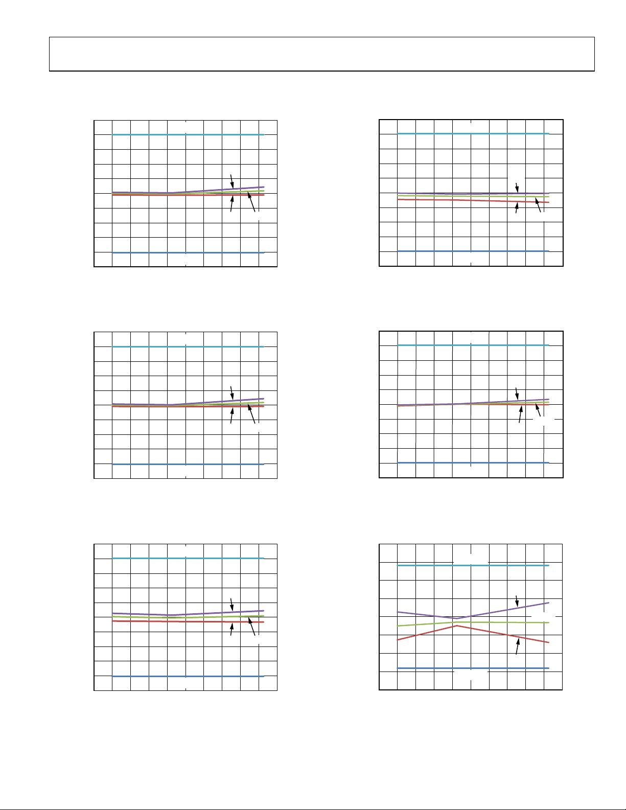
TYPICAL PERFORMANCE CHARACTERISTICS
Figure 5. VS1 ADC Accuracy vs. Temperature (from 10% to 90% of FSR)
Figure 8. CS1 ADC Accuracy vs. Temperature (from 10% to 90% of FSR)
Figure 6. VS2 ADC Accuracy vs. Temperature (from 10% to 90% of FSR)
Figure 7. VS3 ADC Accuracy vs. Temperature (from 10% to 90% of FSR)
Figure 9. CS2 ADC Accuracy vs. Temperature (from 10% to 90% of FSR)
Figure 10. CS1 Fast OCP Threshold vs. Temperature
Rev. A | Page 13 of 96
ADP1046 Data Sheet
2.5
–2.5
–2.0
–1.5
–1.0
–0.5
0
1.0
0.5
1.5
2.0
–60 –40 –20 0 20 40 60 80 100 120 140
ACSNS ADC ACCURACY (%FSR)
TEMPERATURE (°C)
10045-406
MIN
MAX SPEC
MIN SPEC
MEAN
MAX
4
–4
–3
–2
–1
0
1
2
3
–60 –40 –20 0 20 40 60 80 100 120 140
RTD ADC ACCURACY (%FSR)
TEMPERATURE (°C)
10045-408
MAX SPEC
MIN SPEC
MIN
MAX
MEAN
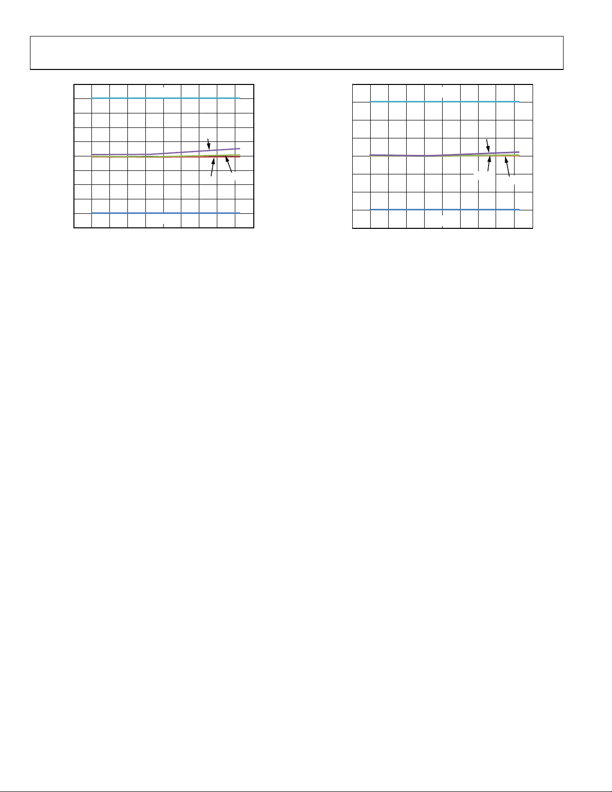
Figure 11. ACSNS ADC Accuracy vs. Temperature (from 10% to 90% of FSR)
Figure 12. RTD ADC Accuracy vs. Temperature (from 10% to 90% of FSR)
Rev. A | Page 14 of 96
Data Sheet ADP1046
CS1
1kΩ 10Ω
I = 100mA
I = 10A
V
IN
OUTA
OUTB
OUTC
OUTD
ADC
12 BITS
V
REF
FAST
OCP
1:100
1V
10045-010
CS2–CS2+
ADC
12 BITS
5.5kΩ 5.5kΩ
1V
I
12V
2mA 2mA
10045-011
CS2+CS2–
ADC
12 BITS
5kΩ 5kΩ
1V
I
200µA 200µA
10045-012
THEORY OF OPERATION
CURRENT SENSE
The ADP1046 has two current sense inputs: CS1 and CS2±.
These inputs sense, protect, and control the primary input
current, secondary output current, and the share bus
information. They can be calibrated to reduce errors due to
external components.
CS1 Operation (CS1)
CS1 is typically used for the monitoring and protection of
the primary side current, which is commonly sensed using a
current transformer (CT). The input signal at the CS1 pin is fed
into an ADC for current monitoring. The range of the ADC is
0 V to 1.4 V. The input signal is also fed into a comparator for
pulse-by-pulse OCP protection. The typical configuration for
the CS1 current sense is shown in Figure 13.
When using low-side current sensing, the current sources are
200 µA; therefore, the required resistor value is 1 V/200 µA = 5 kΩ.
When using high-side current sensing, the current sources are
2 mA; therefore, the resistor value required is (V
In the case of V
= 12 V, the required resistor value is 5.5 kΩ.
OUT
− 1 V)/2 mA.
OUT
Typical configurations are shown in Figure 14 and Figure 15.
Various thresholds and limits can be set for CS2±, such as OCP.
These thresholds and limits are described in the Current Sense
and Current Limit Registers section.
When not in use, the CS2+ and CS2− inputs should both be
connected directly to PGND, and CS2± should be set to highside current sense mode (Register 0x27[2] = 1).
The CS2 ADC is used to measure the CS2 current; the reading
is averaged every 2.62 ms in an asynchronous fashion. This
averaged reading is used to make fault decisions, such as the
CS2 OCP fault. The ADP1046 also writes the 12-bit CS2
reading every 10 ms to Register 0x18.
Figure 13. Current Sense 1 (CS1) Operation
The CS1 ADC is used to measure the average value of the
primary current; the reading is averaged every 2.62 ms in an
asynchronous fashion to make fault decisions. The ADP1046
also writes the 12-bit CS1 reading every 10 ms to Register 0x13.
The fast OCP comparator is used to limit the instantaneous
primary current within each switching cycle and has a nominal
threshold of 1.2 V.
Various thresholds and limits can be set for CS1, as described in
the Current Sense and Current Limit Registers section.
CS2 Operation (CS2+, CS2−)
CS2+ and CS2− are differential inputs used for the monitoring
and protection of the secondary side current. The full-scale
range of the CS2 ADC is programmable to 60 mV or 120 mV.
The differential inputs are fed into an ADC through a pair of
external resistors that provide the necessary level shifting. The
device pins, CS2+ and CS2−, are internally regulated to approximately 1 V by internal current sources.
Figure 14. High-Side Resistive Current Sense
Figure 15. Low-Side Resistive Current Sense (Recommended)
Rev. A | Page 15 of 96
ADP1046 Data Sheet
VS1
VS3+
VS3–
VS2
ADC
PGND
VS3VS2
12 BITS
VS1
12 BITS
DIGITAL
FILTER
1V 1V
12V 12V
11kΩ
1kΩ
1V
LOAD
11kΩ11kΩ
1kΩ 1kΩ
12V
HF
ADC
ADC
VS3
12 BITS
ADC
10045-013
MAGNITUDE
FREQUENCY
NYQUIST ADC
NOISE
Σ-Δ ADC
NOISE
10045-014
195.3
7 bits
VOLTAGE SENSE AND CONTROL LOOP
Multiple voltage sense inputs on the ADP1046 are used for the
monitoring, control, and protection of the power supply output.
This information is available through the I
sense points can be calibrated digitally to minimize errors due to
external components. This calibration can be performed in the
production environment, and the settings can be stored in the
EEPROM of the ADP1046 (see the Power Supply Calibration
and Tri m section for more information).
For voltage monitoring, the VS1, VS2, and VS3 voltage value
registers (Register 0x15, Register 0x16, and Register 0x17,
respectively) are updated every 10 ms. The ADP1046 stores every
ADC sample for 10 ms and then outputs the average value at the
end of the 10 ms period. Therefore, if these registers are read at
least every 10 ms, a true average value is read.
The ADP1046 uses two separate sensing points: VS1 and VS3±,
depending on the condition of the OrFET. When the OrFET is
turned off, the control loop is regulated via VS1; when the OrFET
is turned on, the control loop is regulated via the differential
sensing on VS3±. This sensing mechanism effectively performs
a local and remote voltage sense.
The control loop of the ADP1046 features a patented multipath
architecture. The output voltage is converted simultaneously by
two ADCs: a high accuracy ADC and a high speed ADC. The
complete signal is reconstructed and processed in the digital
filter to provide a high performance, cost competitive solution.
2
C interface. All voltage
Σ-Δ ADCs also differ from Nyquist rate ADCs in that the quantization noise is not uniform across the frequency spectrum. At
lower frequencies, the noise is lower, and at higher frequencies,
the noise is higher (see Figure 17).
Figure 17. Noise Performance for Nyquist Rate and Σ-Δ ADCs
The low frequency ADC runs at approximately 1.56 MHz. For a
specified bandwidth, the equivalent resolution can be calculated
as follows:
ln(1.56 MHz/BW)/ln2 = N bits
For example, at a bandwidth of 95 Hz, the equivalent
resolution/noise is
ln(1.5 MHz/95)/ln2 = 14 bits
At a bandwidth of 1.5 kHz, the equivalent resolution/noise is
ln(1.56 MHz/1.5 kHz)/ln2 = 10 bits
The high frequency ADC has a clock of 25 MHz. It is comb
filtered and outputs at the switching frequency (f
) into the
SW
digital filter. The equivalent resolution at some sample
frequencies is listed in Ta b l e 5.
Figure 16. Voltage Sense Configuration
ADCs
Two kinds of Σ-Δ ADCs are used in the feedback loop of the
ADP1046: a low frequency (LF) ADC that runs at 1.56 MHz
and a high frequency (HF) ADC that runs at 25 MHz.
Σ-Δ ADCs have a resolution of one bit and operate differently
from traditional flash ADCs. The equivalent resolution obtainable depends on how long the output bit stream of the Σ-Δ is
sampled.
Table 5. Equivalent Resolutions for High Frequency ADC
at Various Switching Frequencies
fSW (kHz) High Frequency ADC Resolution
48.8 9 bits
97.7 8 bits
390.6 6 bits
The HF ADC has a range of ±30 mV. Using a base switching
frequency (f
increases to 200 kHz (7-bit HF ADC resolution), the quantization
noise is 0.9375 mV (1 LSB). Increasing f
quantization noise to 3.75 mV (1 LSB = 2 × 30 mV/2
VS1 OPERATION (VS1)
Rev. A | Page 16 of 96
VS1 is used for the monitoring and protection of the power supply
voltage at the output of the LC stage, upstream of the OrFET. The
VS1 sense point on the power rail needs an external resistor
divider to bring the nominal input voltage to 1 V at the VS1 pin
(see Figure 16). The resistor divider is necessary because the VS1
ADC input range is 0 V to 1.6 V (12-bit reading). This divideddown signal is internally fed into a low speed Σ-Δ ADC. The output
of the VS1 ADC goes to the digital filter and is also updated in
Register 0x15 every 10 ms. The VS1 signal is referenced to PGND.
When the OrFET is turned off, the power supply is regulated
from the VS1 sense point instead of the VS3± sense point.
) of 100 kHz (8-bit HF ADC resolution), when fSW
SW
to 400 kHz increases the
SW
6
= 0.9375 mV).
Data Sheet ADP1046
ACSNS
ADC
0V TO 1.6V
ACSNS
FEEDFORWARD
ADC
0.6V TO 1. 6V
PROGRAMMABLE
ACTION (REG 0x0D[3:0])
FEEDFORWARD
GAIN
(REG 0x75[1:0])
DPWM
ENGINE
DIGITAL
FILTER
ACSNS GAIN TRIM
(REG 0x5E)
0.45V
1/x
Vx
R1
R2
FROM
SECONDARY
WINDING
10045-015
R
ACSNS
DIGITAL
FILTER
OUTPUT
OUTx
t
MODULATION
t
S
t
S
t
MODULATION
10045-016
−
−
×+
−
×
×
=
az
bz
c
z
z
m
d
H(z)
68.7124.202
VS2 OPERATION (VS2)
VS2 is used in conjunction with VS1 to control the OrFET gate
drive turn-on. The VS2 sense point on the power rail needs an
external resistor divider to bring the nominal common-mode
signal to 1 V at the VS2 pin (see Figure 16).
The resistor divider is necessary because the VS2 ADC input
range is 0 V to 1.6 V. This divided-down signal is internally fed
into the VS2 ADC. The output of the VS2 ADC goes to the VS2
voltage value register (Register 0x16). The VS2 signal is never
used for the control loop but is used to control the turn-on and
turn-off of the OrFET (see the OrFET Control (GATE) section)
as well as the voltage continuity flag. If the OrFET function of
the ADP1046 is not used, it is recommended that the VS2 input
be connected directly to PGND. The VS2 value is updated in
Register 0x16 every 10 ms.
VS3 OPERATION (VS3+, VS3−)
VS3± is used for the monitoring and protection of the remote
load voltage. VS3± is a fully differential input that is the main
feedback sense point for the power supply control loop. The
VS3± sense point on the power rail needs an external resistor
divider to bring the nominal common-mode signal to 1 V at
the VS3± pins (see Figure 16). The resistor divider is necessary
because the VS3 ADC input range is 0 V to 1.6 V. This divideddown signal is internally fed into a high frequency (HF) ADC.
The output of the VS3 ADC goes to the digital filter and is also
updated in Register 0x17 every 10 ms. The HF ADC is also the
high frequency feedback loop for the power supply.
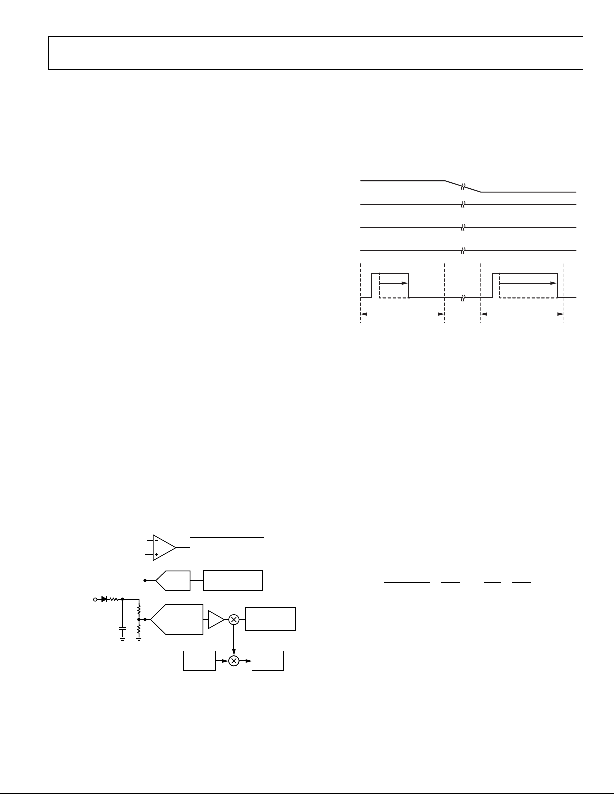
VOLTAGE LINE FEEDFORWARD AND ACSNS
The ADP1046 supports voltage line feedforward control to
improve line transient performance. The ACSNS value is used
to divide the output of the digital filter, and the result is fed into
the PWM engine. The input voltage signal can be sensed at the
secondary winding of the isolation transformer and must be
filtered by an RCD network to eliminate the voltage spike at the
switch node (see Figure 18).
The feedforward scheme modifies the modulation value based
on the ACSNS voltage. When the ACSNS input is 1 V, the line
feedforward has no effect. For example, if the digital filter output
remains unchanged and the ACSNS voltage changes to 50% of
its original value (still higher than 0.5 V), the modulation of the
falling edge of OUTx doubles and vice versa (see Figure 19). The
voltage line feedforward function is optional and is programmable
using Register 0x75.
Figure 19. Feedforward Control on Modulation
The ACSNS level comparator is also connected on the same pin
and flags an ACSNS fault when the voltage on the pin is below
0.45 V within each switching period. The ACSNS level comparator
is used to detect whether the node is switching.
DIGITAL FILTER
The loop response of the power supply can be changed using the
internal programmable digital filter. A Type 3 filter architecture
has been implemented. To tailor the loop response to the specific
application, the low frequency gain, zero location, pole location,
and high frequency gain can all be set individually (see the Digital
Filter Programming Registers section). It is recommended that
the Analog Devices, Inc., software GUI be used to program the
filter. The software GUI displays the filter response in Bode plot
format and can be used to calculate all stability criteria for the
power supply.
From the sensed voltage to the duty cycle, the transfer function
of the filter in z-domain is as follows:
Figure 18. Feedforward Configuration
The ACSNS voltage must be set to 1 V when the nominal input
voltage is applied. The ACSNS ADC sampling period is 10 µs;
therefore, the decision to modify the PWM outputs based on
input voltage is performed at this rate.
where:
a = filter_pole_register_value/256.
b = filter_zero_register_value/256.
c = high_frequency_gain_register_value.
d = low_frequency_gain_register_value.
m = 1 when 48.8 kHz ≤ f
m = 2 when 97.7 kHz ≤ f
m = 4 when 195.3 kHz ≤ f
m = 8 when 390.6 kHz ≤ f
where f
Rev. A | Page 17 of 96
< 97.7 kHz.
SW
< 195.3 kHz.
SW
< 390.6 kHz.
SW
.
SW
is the switching frequency.
SW
ADP1046 Data Sheet
sf
sf
z(s)
SW
SW
−
+
=
2
2
ISOLATORDRIVER
DRIVER
OUTA
OUTB
OUTC
OUTD
SR1 SR2
V
IN
OUTA
OUTD
OUTC
OUTB
SR1
SR2
10045-117
To transfer the z-domain value to the s-domain, plug the following bilinear transformation equation into the H(z) equation:
The digital filter introduces an extra phase delay element into
the control loop. The digital filter circuit sends the duty cycle
information to the PWM circuit at the beginning of each switching cycle (unlike an analog controller, which makes decisions on
the duty cycle information continuously). Therefore, the extra
phase delay for phase margin, Φ, introduced by the filter block is
Φ = 360 × (f
C/fSW
)
where:
f
is the crossover frequency.
C
f
is the switching frequency.
SW
At one-tenth the switching frequency, the phase delay is 36°.
The GUI incorporates this phase delay into its calculations.
Note that the GUI does not account for other delays such as
gate driver and propagation delays.
Two sets of registers allow for two distinct filter responses.
The main filter, called the normal mode filter, is controlled by
programming Register 0x60 to Register 0x63. The light load
mode filter is controlled by programming Register 0x64 to
Register 0x67. The ADP1046 uses the light load mode filter
only when the output current measured on CS2± is below the
load current threshold (programmed using Register 0x3B[2:0]).
The Analog Devices software GUI allows the user to program the
light load mode filter in the same manner as the normal mode
filter. It is recommended that the GUI be used for this purpose.
In addition, during the soft start process, a soft start filter can
be used in combination with the normal mode filter and the
light load mode filter. The soft start filter is programmed using
Register 0x71 to Register 0x74. For more information, see the
Soft Start section.
Filter Transitions
To avoid output voltage glitches and provide a seamless
transition from one filter to another, the ADP1046 supports
programmable filter transitions. This feature allows a gradual
transition from one filter to another. Filter transitions are
programmed using Register 0x7A[2:0].
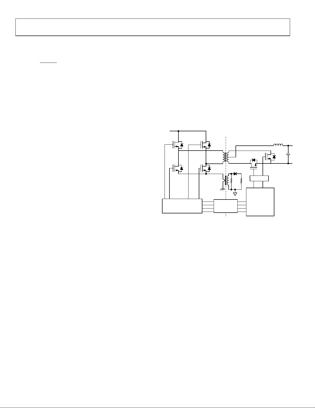
PWM AND SYNC RECT OUTPUTS (OUTA, OUTB, OUTC, OUTD, OUTAUX, SR1, SR2)
The PWM and SR outputs are used for control of the primary
side drivers and the synchronous rectifier drivers. These outputs
can be used for several control topologies such as full-bridge,
phase-shifted ZVS configurations and interleaved, two switch
forward converter configurations. Delays between rising and
falling edges can be individually programmed. Special care
must be taken to avoid shootthrough and cross-conduction.
It is recommended that the Analog Devices software GUI be
used to program these outputs. Figure 20 shows an example
configuration to drive a full-bridge, phase-shifted topology
with synchronous rectification.
Figure 20. PWM Pin Assignment for Full-Bridge, Phase-Shifted Topology
with Synchronous Rectification
The PWM and SR outputs are all synchronized with each
other. Therefore, when reprogramming more than one of these
outputs, it is important to first update all the registers and then
latch the information into the ADP1046 at the same time. During
reprogramming, the outputs are temporarily disabled. A special
instruction is sent to the ADP1046 to ensure that new timing
information is programmed simultaneously. This is done by
setting Bit 1 in Register 0x7F. It is recommended that PWM
outputs be disabled when not in use.
OUTAUX is an additional PWM output pin. OUTAUX allows
an extra PWM signal to be generated at a different frequency
from the other six PWM outputs. This signal can be used to
drive an extra power converter stage, such as a buck controller
located in front of a full-bridge converter. OUTAUX can also
be used as a clock reference signal.
For more information about the various programmable switching
frequencies and PWM timings, see the PWM and Synchronous
Rectifier Timing Registers section (Register 0x3F to Register 0x5C).
Rev. A | Page 18 of 96

OUTx
t
MODULATION_LIMIT
t
RX
t
FX
10045-118
Data Sheet ADP1046
SYNCHRONOUS RECTIFICATION
SR1 and SR2 are recommended for use as the PWM control
signals when using synchronous rectification. These PWM
signals can be configured much like the other PWM outputs.
An optional soft start can be applied to the synchronous
rectifier PWM outputs. The SR soft start can be programmed
using Register 0x54[1:0].
• When SR soft start is disabled (Register 0x54[0] = 0),
the SR signals are turned on to their full PWM duty cycle
values immediately.
• When SR soft start is enabled (Register 0x54[0] = 1), the
SR signals ramp up from zero duty cycle to the desired
duty cycle in steps of 40 ns per switching cycle.
The advantage of ramping the SR signals is to minimize the
output voltage step that occurs when the SR FETs are turned
on without a soft start. The advantage of turning the SR signals
completely on immediately is that they can help to minimize
the voltage transient caused by a load step.
Using Register 0x54[1], the SR soft start can be programmed to
occur only once (the first time that the SR signals are enabled)
or every time that the SR signals are enabled, for example, when
the system enters or exits light load mode.
When programming the ADP1046 to use SR soft start, ensure
correct operation of this function by setting the falling edge of
SR1 (t
) to a lower value than the rising edge of SR1 (t9) and by
10
setting the falling edge of SR2 (t
edge of SR2 (t
). SR soft start can also be disabled by setting
11
) to a lower value than the rising
12
Register 0x0F[7] = 1.
SR (SYNCHRONOUS RECTIFIER) DELAY
The ADP1046 is well suited for dc-to-dc converters in isolated
topologies. Every time a PWM signal crosses the isolation barrier
an additional propagation delay is added due to the isolating
components. The ADP1046 allows programming of an adjustable
delay (0 ns to 315 ns in steps of 5 ns) using Register 0x79[5:0]. This
delay moves both SR1 and SR2 later in time to compensate for the
added delay due to the isolating components (see Figure 56). In
this way, the edges of all PWM outputs can be aligned, and the
SR delay can be applied separately as a constant dead time.
ADAPTIVE DEAD TIME CONTROL
A set of registers called the adaptive dead time (ADT) registers
(Register 0x68 to Register 0x70) allows the dead time between
PWM edges to be adapted on the fly. The ADP1046 uses the ADT
only when the modulation is below the dead time (primary
current) threshold programmed in Register 0x68. The Analog
Devices software GUI allows the user to easily program the dead
time values, and it is recommended that the GUI be used for
this purpose.
Before ADT is configured, the primary current threshold must
be programmed. Each individual PWM rising and falling edge
(t
to t14) can then be programmed to have a specific dead time
1
offset at no load (zero current).
Rev. A | Page 19 of 96
This offset can be positive or negative and is relative to the nominal
edge position. When the CS1 current is between zero and the
current threshold, the amount of dead time is linearly adjusted
in steps of 5 ns. The averaging period of the CS1 current and
the speed of the dead time adjustment can also be programmed
in Register 0x70 to accommodate faster or slower adjustment.
For example, if the CS1 threshold is set to 2 A, t
rising edge of 100 ns. If the ADT setting for t
t
moves to 140 ns when the current is 0 A and to 120 ns when
1
has a nominal
1
is 40 ns at no load,
1
the current is 1 A. Similarly, ADT can be applied in the negative
direction.
LIGHT LOAD MODE
The ADP1046 can be configured to disable PWM outputs under
light load conditions based on the value of CS2. Register 0x3B
and Register 0x7D are used to program the light load mode
thresholds for turn-off and turn-on of SR1, SR2, and other
PWM outputs. Below the light load threshold programmed in
Register 0x3B, the SR outputs are disabled; the user can also
program any of the other PWM outputs to shut down below
this threshold. Light load mode allows the ADP1046 to be used
with interleaved topologies that incorporate automatic phase
shedding at light load.
To prevent the system from oscillating between light load
and normal modes due to the thresholds being programmed
too close to each other, a programmable debounce is provided
in Register 0x7D[5:4]. This debounce prevents the part from
changing state within the programmed interval.
The speed of the SR enable is programmable from 37.5 µs to 300 µs
in four discrete steps using Register 0x7D[3:2]. This ensures that,
in case of a load step, the SR signals (and any other PWM outputs
that are temporarily disabled) can be turned on quickly enough to
prevent damage to the FETs that they are controlling.
The light load mode digital filter is also used during light
load mode.
MODULATION LIMIT
The modulation limit register (Register 0x2E) can be
programmed to apply a maximum duty cycle modulation limit
to any PWM signal, thus limiting the modulation range of any
PWM output. When modulation is enabled, the maximum
modulation limit is applied to all PWM outputs collectively. As
shown in Figure 21, this limit is the maximum time variation
for the modulated edges from the default timing, following the
configured modulation direction. There is no minimum duty
cycle limit setting. Therefore, the user must set the rising edges
and falling edges based on the case with the least modulation.
Figure 21. Modulation Limit Settings

ADP1046 Data Sheet
10045-119
Each LSB in Register 0x2E corresponds to a different time step
size, depending on the switching frequency (see Tab l e 46). The
modulated edges cannot extend beyond one switching cycle.
The GUI provided with the ADP1046 is recommended for
programming this feature (see Figure 22).
Figure 22. Setting Modulation Limits (Modulation Range Shown by Arrows)
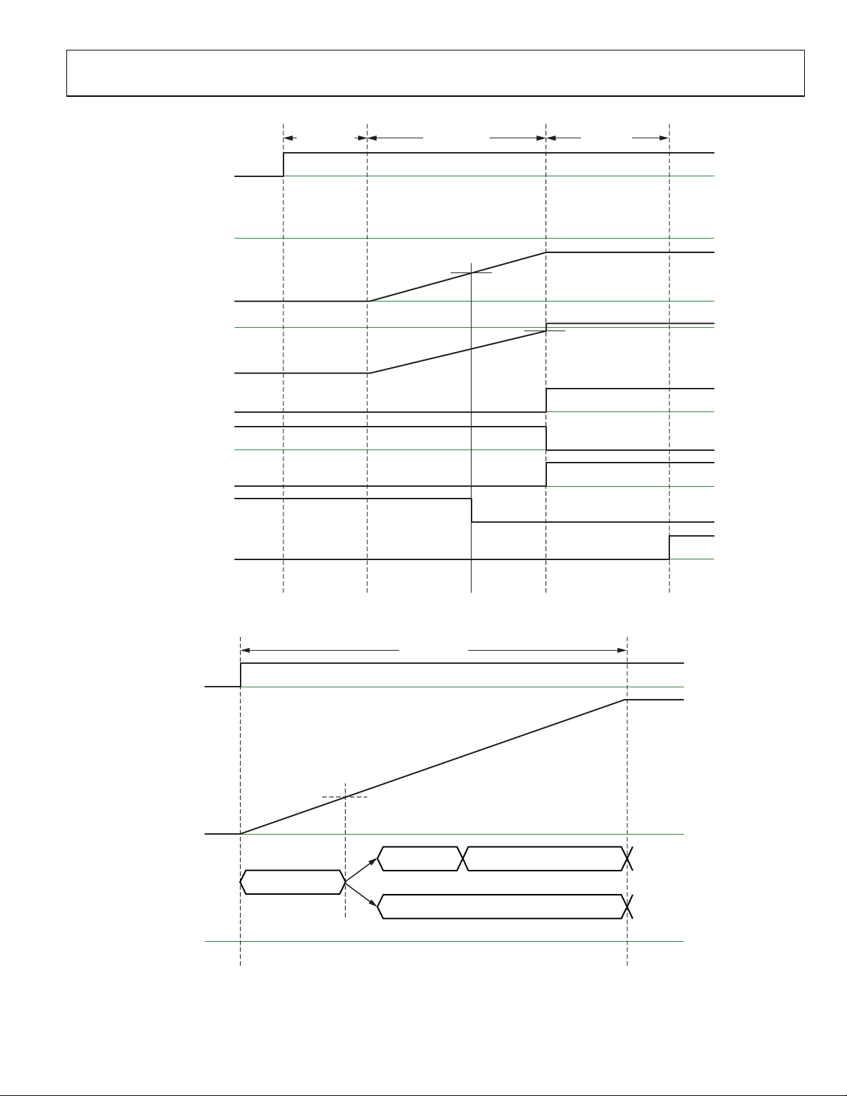
SOFT START
The turning on and off of the ADP1046 is controlled by the
hardware PSON pin and/or the software PSON register,
depending on the configured settings in Register 0x2C.
When the user turns on the power supply (enables PSON),
the following soft start procedure occurs (see Figure 23).
1. The PSON signal is enabled at Time t
programmed to be always on (Register 0x2C[7:6] = 00),
PSON is enabled as soon as VCORE is above UVLO.
2. The ADP1046 waits for the programmed PS_ON delay
(set in Register 0x2C[4:3]).
3. The soft start begins to ramp up the internal digital refer-
ence. The total duration of the soft start ramp is programmable from 5 ms to 100 ms using Register 0x5F[7:5].
4. If the soft start from precharge function is enabled
(Register 0x5F[4] = 1), the soft start ramp starts from
the value of the output voltage sensed on VS1 or VS3±
(depending on the OrFET status), and the soft start ramp
time is reduced proportionally. If the soft start from precharge function is disabled, the soft start ramp time is the
programmed value in Register 0x5F[7:5].
5. When the power supply voltage exceeds the VS1 under-
voltage protection (UVP) limit (set in Register 0x34[6:0]),
the UVP flag is reset.
6. The OrFET is turned on as soon as the OrFET enable thresh-
old is met. (The OrFET enable threshold is programmed in
Register 0x30[6:5].) The regulation point is switched from
VS1 to VS3±.
7. If no other fault conditions are present, the PGOODx
signals wait for the programmed debounce time (set in
Register 0x2D[7:4]) and are then enabled. The soft start
flag must be unmasked in Register 0x7B and Register 0x7C
(Bit 7 must be set to 0).
8. If no OrFET is used, the power supply must be configured
to regulate using VS3 at all times (Register 0x33[2] = 1).
VS2 can be used as a secondary OVP mechanism.
. If the part is
0
Fault Condition During Soft Start
If a fault condition occurs during soft start, the controller responds
as programmed unless the flag is blanked. Flag blanking during
soft start is programmed in Register 0x0F. The UVP and ACSNS
flags are always blanked during soft start. The OTP, FLAGIN,
OVP, and OCP fault flags can be blanked during soft start by
setting the appropriate bits in Register 0x0F.
Digital Compensation Filters During Soft Start
The ADP1046 has a dedicated soft start filter (SSF) that can be
used to fine-tune and optimize the dynamic response during
the output voltage ramp-up.
Before it ramps up the internal reference after the PSON signal
is enabled, the ADP1046 evaluates whether the OrFET should
be turned on or off by looking at the difference between VS1
and VS2. This step is done to determine whether the regulation
point should be VS1 or VS3± (see Figure 23).
• If the regulation point is VS1, the soft start filter is used
by default during the ramp-up. At the end of the soft start
ramp, the part switches to the normal mode filter (NMF).
• If the regulation point is VS3±, the part starts the ramp
using the normal mode filter (NMF).
In both cases, after the voltage reaches 12.5% of the nominal
output voltage value, the load current is evaluated.
• If the load current is below the light load mode threshold,
the part switches to the light load mode filter (LLF).
• If the load current is above the light load mode threshold,
the normal mode filter is used until the end of the soft start
ramp, even if the system subsequently enters light load
mode based on a change to the load current.
Register 0x2C can be programmed to configure the use of the
different filters during soft start as follows:
• Force soft start filter (Bit 0). This option forces the part to
use the soft start filter even when the regulation point is
VS3. In some cases, this option allows better fine-tuning of
the ramp-up voltage. This option can also be selected when
an OrFET is not used.
• Disable light load mode during soft start (Bit 1). This
option prevents the use of the light load mode filter during
soft start, even if the light load condition is met. The light
load mode filter is available for use after the end of the soft
start ramp.
Rev. A | Page 20 of 96
Data Sheet ADP1046
OrFET E NABLE
UVP
t
0
PSON
VS3
VS1
(VS1 – VS2)
VOLTAGE
OrFET GATE
LOOP CONTROLLED
FROM VS1
LOOP CONTROLLED
FROM VS3
UVP FLAG
PGOOD1
PS_ON DELAY
(REG 0x2C[4:3])
RAMP TIME
(REG 0x5F[7: 5] )
PGOOD DE BOUNCE
(REG 0x2D)
10045-120
PSON
V
OUT
RAMP TIME
(REG 0x5F[7: 5] )
12.5% REF
LIGHT LOAD
FILTER (LLF)
NORMAL MODE FILTER (NMF)
OR SOFT START FILTER (SSF)
NORMAL MODE FILTER (NMF)
OR SOFT START FILTER (SSF)
NORMAL MODE FILTER (NMF)
OR SOFT START FILTER (SSF)
LLF OR NMF
BASED ON
LOAD
LLF OR NMF
BASED ON
LOAD
10045-121
Figure 23. Soft Start Timing Diagram
Figure 24. Filter Sequencing at Startup
Rev. A | Page 21 of 96
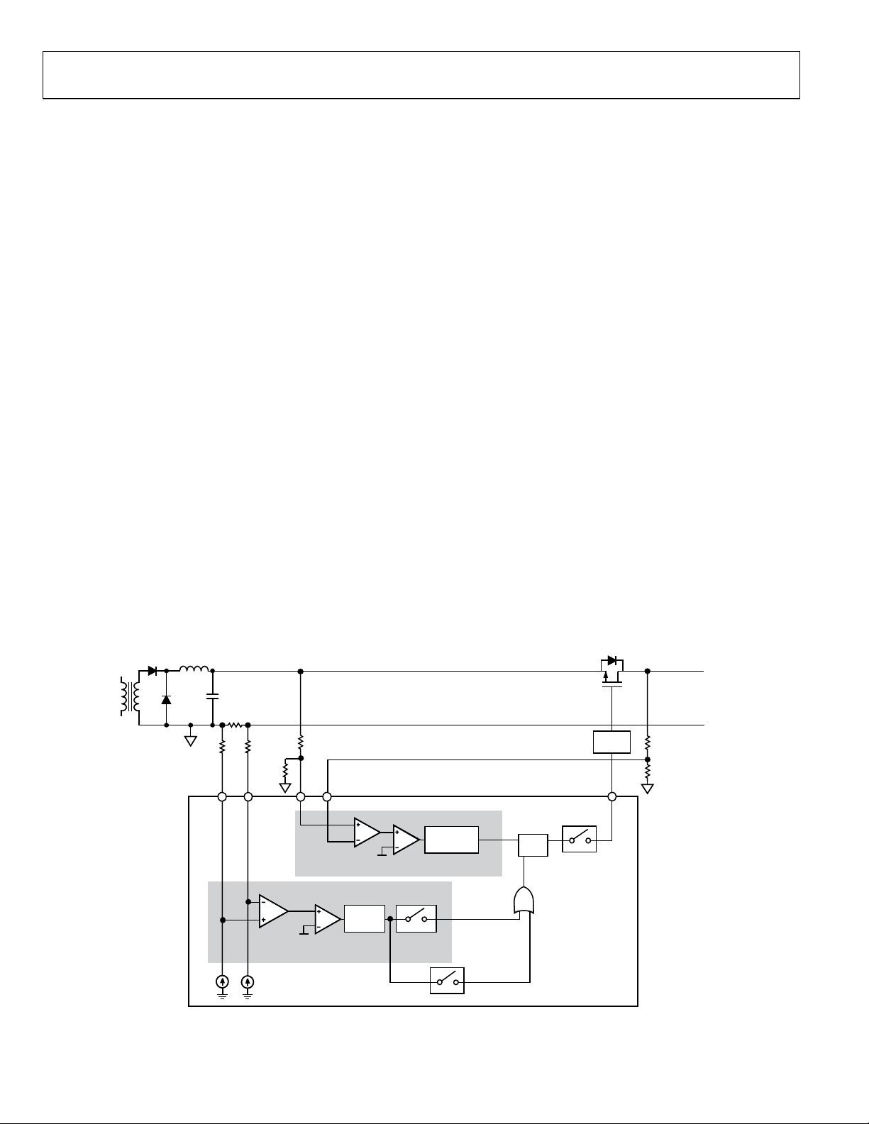
ADP1046 Data Sheet
FAST OrFET
COMPARATOR
FAST OrFET
THRESHOLD
OrFET
DISABLE
CS2– CS2+
12V
11kΩ
11kΩ
1kΩ
1kΩ
V
OUT
VS2VS1
R
SENSE
GATE
FAST OrFET
BYPASS
FAST OrFET
DEBOUNCE
S
R
Q
OrFET
ENABLE
OrFET
ENABLE THRES HOLD
FLAGS
DRIVER
DEBOUNCE
GATE
DISABLE
10045-122
ORFET CONTROL (GATE)
The GATE control signal drives an external OrFET. The OrFET
is used in redundant systems to protect against power flow into
the power supply from another supply’s output terminals. This
ensures that power flows only out of the power supply and that
the unit can be hot-swapped.
The GATE pin is a totem-pole output and does not require a
pull-up resistor. The GATE pin polarity can be programmed via
Register 0x2D[1] to be active high or active low. The GATE output is CMOS level (0 V to 3.3 V). An external driver is required
to turn the OrFET on or off.
OrFET Turn-On
The turn-on process for the OrFET is controlled by the voltage
difference between VS1 and VS2. For this reason, the VS1 and
VS2 readings must be correctly calibrated for the OrFET function to perform properly.
The OrFET turn-on circuit detects the voltage difference between
VS1 and VS2 (see Figure 25). When the forward voltage drop from
VS1 to VS2 is greater than the programmable OrFET enable
threshold set in Register 0x30[6:5], the OrFET is enabled. The
OrFET enable threshold can be set to 0%, −0.5%, −1%, or −2%
of the nominal output voltage.
OrFET Turn-Off
The OrFET can be turned off by three methods:
• Fault flag. Any flag in a fault configuration register
(Register 0x08 to Register 0x0D) can be programmed with
an action to turn off the OrFET. The OrFET is kept off for
as long as the flag is set.
• OrFET programmable comparator. If the reverse voltage
present on CS2± exceeds the analog comparator threshold
programmed in Register 0x30[4:2], the OrFET is turned off.
This comparator can be disabled using Register 0x30[0].
• GATE signal disable. When Register 0x5D[0] = 1, the
GATE signal is disabled and has no effect on the VSx
feedback point.
OrFET GATE Control and Regulation Points
The GATE signal is enabled when the threshold configured
in Register 0x30[6:5]) is met. The GATE signal controls a very
important function of output voltage regulation: the control
loop sensing point.
• When the GATE signal is disabled, the OrFET is turned off
and the voltage regulation sensing point is VS1.
• When the GATE signal is enabled, the OrFET is turned on
and the voltage regulation sensing point is VS3±.
Recommended Setup for a 12 V Application
In normal operating mode, follow this procedure:
• When 12 V < V
< OVP, use the fast OrFET control
OUT
circuit to turn off the Or FE T.
• When V
> OVP, use load OVP to turn off the OrFET.
OUT
In light load mode, follow this procedure:
• When 12 V < V
< OVP, use ACSNS to turn off the
OUT
OrF ET.
• When V
> OVP, use load OVP to turn off the OrFET.
OUT
In a 12 V application, when an internal short circuit occurs, use
CS1 OCP or VS1 UVP to shut down the unit and restart it.
Figure 25. OrFET Control Circuit Internal Detailed Diagram
Rev. A | Page 22 of 96
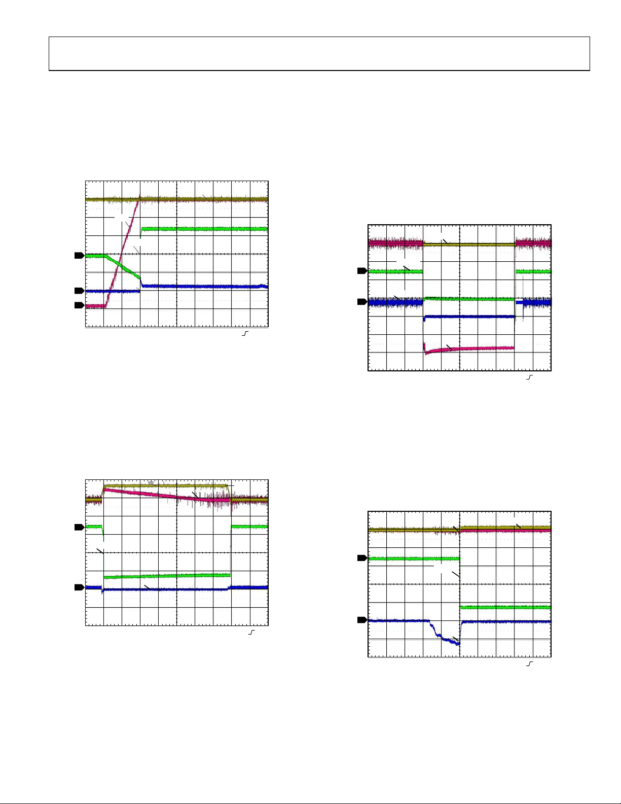
Data Sheet ADP1046
CH2 2.00V
CH4 10.0V
CH1 2.00V
CH3 2.00A
M10.0ms A CH4 100mV
2
3
4
CS2
VS3
VS1
OrFET
10045-017
CH2 2.00V
CH4 10.0V
CH1 2.00V
CH3 2.00A
M50.0ms A CH4 0mV
3
4
CS2
VS3
VS1
OrFET
10045-018
CH2 2.00V
CH4 10.0V
CH1 2.00V
CH3 2.00A
M200.0ms A CH4 7.5mV
3
4
CS2
VS3
OrFET
VS1
10045-019
CH2 2.00V
CH4 10.0V
CH1 2.00V
CH3 2.00A
M5.0ms A CH4 8.3mV
3
4
CS2
VS3
OrFET
VS1
10045-020
OrFET Operation Examples
Hot Plug into a Live Bus
A new PSU is plugged into a live 12 V bus (yellow). The internal
voltage, VS1 (red), is ramped up before the OrFET is turned on.
After the OrFET is turned on (green), current in the new PSU
begins to flow to the load (blue). The turn-on voltage threshold
between the new PSU and the bus is programmable.
Short Circuit
When one of the output rectifiers fails, the bus voltage can
collapse if the OrFET is not promptly turned off. The fast OrFET
comparator is used to protect the system from this fault event.
Figure 28 shows a short circuit applied to the output capacitors
before the OrFET. After the fast OrFET threshold for CS2± (blue)
is triggered, the OrFET (green) is turned off. Figure 28 also shows
the operation when the short circuit is removed. The internal
regulation point, VS1 (red), returns to 12 V, and the OrFET
(green) is reenabled. The PSU again begins to contribute
current to the load (blue).
Figure 26. Hot Plug into a Live Bus (Yellow Is Bus Voltage; Red Is VS1 Voltage;
Green Is OrFET Control Signal; Blue Is Load Current)
Runaway Master
A rogue PSU on the bus (yellow) has a fault condition, causing
the bus voltage to increase above the OVP threshold. The good
PSU turns off the OrFET (green) and regulates its internal voltage, VS1 (red). When the rogue power supply fault condition is
removed, the bus voltage decreases. The OrFET of the good PSU
is immediately turned on, and the good PSU resumes regulating
from VS3±.
Figure 28. Internal Short Circuit (Yellow Is Bus Voltage; Red Is VS1 Voltage;
Green Is OrFET Control Signal; Blue Is Load Current)
Light Load Mode Operation
PSU 1 increases its voltage at light load from 12 V to 12.1 V
(yellow). Both PSU 1 and PSU 2 are CCM; therefore PSU 1
sources current and PSU 2 sinks current (blue). In PSU 2, the
OrFET control turns off the OrFET to prevent reverse current
from flowing. Note that the OrFET voltage (green) is solid during
this transition because PSU 1 and PSU 2 are in CCM mode.
Figure 27. Runaway Master (Yellow Is Bus Voltage; Red Is VS1 Voltage;
Green Is OrFET Control Signal; Blue Is Load Current)
Figure 29. Light Load Mode (Yellow Is Bus Voltage; Red Is VS1 Voltage;
Green Is OrFET Control Signal; Blue Is Load Current)
Rev. A | Page 23 of 96

ADP1046 Data Sheet
PGOOD1
(FLAG AND P IN)
PGOOD2
(FLAG AND P IN)
ADDITIONAL FLAGS
-VOLTAGE CONTINUITY
-OrFET DISABLE
-ACSNS
-FLAGIN
-OTP
MASKED BY
REG 0x7B
MASKED BY
REG 0x7C
DEBOUNCE
(REG 0x2D[7:6])
DEBOUNCE
(REG 0x2D[5:4])
10045-127
MAIN FLAGS
-SOFT START
-CS1 FAST OCP
-CS1 ACCURATE OCP
-CS2 ACCURATE OCP
-UVP
-LOCAL OVP
(FAST AND ACCURAT E )
-LOAD OVP
-OrFET (GATE PIN)
IF REG 0x2D[ 3] = 0, THE
ADDITIONAL FLAGS
ALWAYS AFFECT PGOOD2,
REGARDLESS OF THE
PROGRAMME D ACTION.
IF REG 0x2D[ 3] = 1, THE
ADDITIONAL FLAGS AFFECT
PGOOD2 ONLY IF THEY ARE
NOT SET TO BE IGNORED.
VDD
When VDD is applied, a certain time elapses before the part is
capable of regulating the power supply. When VDD rises above
the power-on reset and UVLO levels, it takes approximately
20 μs for VCORE to reach its operational point of 2.5 V. T h e
EEPROM contents are then downloaded to the registers. The
download takes an additional 25 μs (approximately). After the
EEPROM download, the ADP1046 is ready for operation.
If the ADP1046 is programmed to power up at this time (PSON
is enabled), the soft start ramp begins. Otherwise, the part waits
for the PSON signal.
The proper amount of decoupling capacitance must be placed
between VDD and AGND, as close as possible to the device to
minimize the trace length. It is recommended that the VCORE
pin not be used as a reference or to generate other logic levels
using resistive dividers.
VDD/VCORE OVLO
The ADP1046 has built-in overvoltage protection (OVP) on
its supply rails. When the VDD or VCORE voltage rises above
the OVLO threshold, the response can be programmed using
Register 0x0E[7:5]. It is recommended that when a VDD/
VCORE OVP fault occurs, the response be set to download the
EEPROM before restarting the part (set Register 0x0E[6] = 1).
POWER GOOD
The ADP1046 has two open-drain power-good pins. The
PGOOD1 pin is driven low when a PGOOD1 fault condition
is present; the PGOOD2 pin is driven low when a PGOOD2
fault condition is present. The PGOOD1 and PGOOD2 pins
and flags can be programmed to respond to the following flags:
• Soft start
• CS1 fast OCP
• CS1 accurate OCP
• CS2 accurate OCP
• UVP
• Local OVP (fast and accurate)
• Load OVP
• OrFET (GATE pin )
The masking of these flags is programmed in Register 0x7B
(for PGOOD1) and Register 0x7C (for PGOOD2). When a flag
is masked, it does not set PGOOD1 or PGOOD2.
The following additional flags can also set the PGOOD2 pin either
unconditionally or based on the flag response, as programmed
in Register 0x2D[3] (see Figure 30 and Table 45).
• Voltage continuity
• OrFET disable
• ACSNS
• External flag (FLAGIN pin)
• OTP
These additional flags can be programmed in Register 0x2D[3]
to always set PGOOD2 or to set PGOOD2 only if the flag action
is not set to “ignore” in the fault configuration register for that
flag (see Table 12 and Table 13).
Figure 30. PGOOD1, PGOOD2 Programming
Rev. A | Page 24 of 96
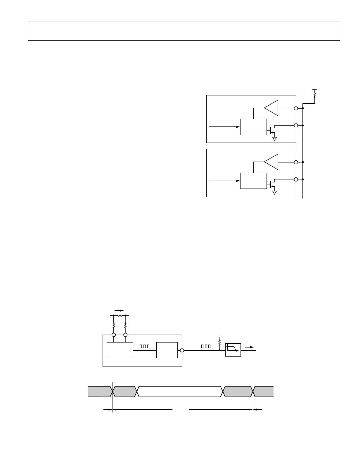
Data Sheet ADP1046
DIGITAL
WORD
SHARE
BUS
CURRENT SENSE
INFO
SHAREi
SHAREo
POWER SUPPLY A
DIGITAL
WORD
CURRENT SENSE
INFO
SHAREi
SHAREo
POWER SUPPLY B
V
DD
10045-023
CURRENT
SENSE
ADC
SHARE
BUS
LPF
BIT STRE AM BIT STRE AM
SHAREo
VOLTAGE
CURRENT
CS2–CS2+
10045-222
8-BIT DATA
PREVIOUS
FRAME
START BIT
0
2 STOP BITS
(IDLE)
START BIT
0
2 STOP BITS
(IDLE)
NEXT FRAME
FRAME
10045-024
CURRENT SHARING (SHARE)
The ADP1046 supports both analog current sharing and digital
current sharing. The ADP1046 can use either the CS1 current
information or the CS2 current information for current sharing
(this setting is programmed in Register 0x29[3]).
Analog Current Sharing
Analog current sharing uses the internal current sensing
circuitry to provide a current reading to an external current
error amplifier. Therefore, an additional differential current
amplifier is not necessary.
The current reading from CS1 or CS2 can be output to the
SHAREo pin in the form of a digital bit stream, which is the
output of the current sense ADC (see Figure 32). The bit stream
is proportional to the current delivered by this unit to the load.
By filtering this digital bit stream using an external RC filter, the
current information is turned into an analog voltage that is
proportional to the current delivered by this unit to the load. This
voltage can be compared to the share bus voltage. If the unit is not
supplying enough current, an error signal can be applied to the
VS3± feedback point. This signal causes the unit to increase its
output voltage and, in turn, its current contribution to the load.
Digital Share Bus
The digital share bus scheme is similar in principle to the traditional analog share bus scheme. The difference is that instead of
using a voltage on the share bus to represent current, a digital
word is used.
The ADP1046 outputs a digital word onto the share bus. The
digital word is a function of the current that the power supply is
providing (the higher the current, the larger the digital word).
The power supply with the highest current controls the bus
(master). A power supply that is putting out less current (slave)
sees that another supply is providing more power to the load
than it is.
During the next cycle, the slave increases its current output contribution by increasing its output voltage. This cycle continues
until the slave outputs the same current as the master, within
a programmable tolerance range. Figure 31 shows the configuration of the digital share bus.
Figure 31. Digital Current Share Configuration
The digital share bus is based on a single-wire communication
bus principle; that is, the clock and data signals are contained
together.
When two or more ADP1046 devices are connected, they synchronize their share bus timing. This synchronization is performed
by the start bit at the beginning of a communications frame. If a
new ADP1046 is hot-swapped onto an existing digital share bus,
the device waits to begin sharing until the next frame. The new
ADP1046 monitors the share bus until it sees a stop bit, which
designates the end of a share frame. It then performs synchronization with the other ADP1046 devices during the next start bit.
The digital share bus frame is shown in Figure 33.
Figure 32. Analog Current Share Configuration
Figure 33. Digital Current Share Frame Timing Diagram
Rev. A | Page 25 of 96
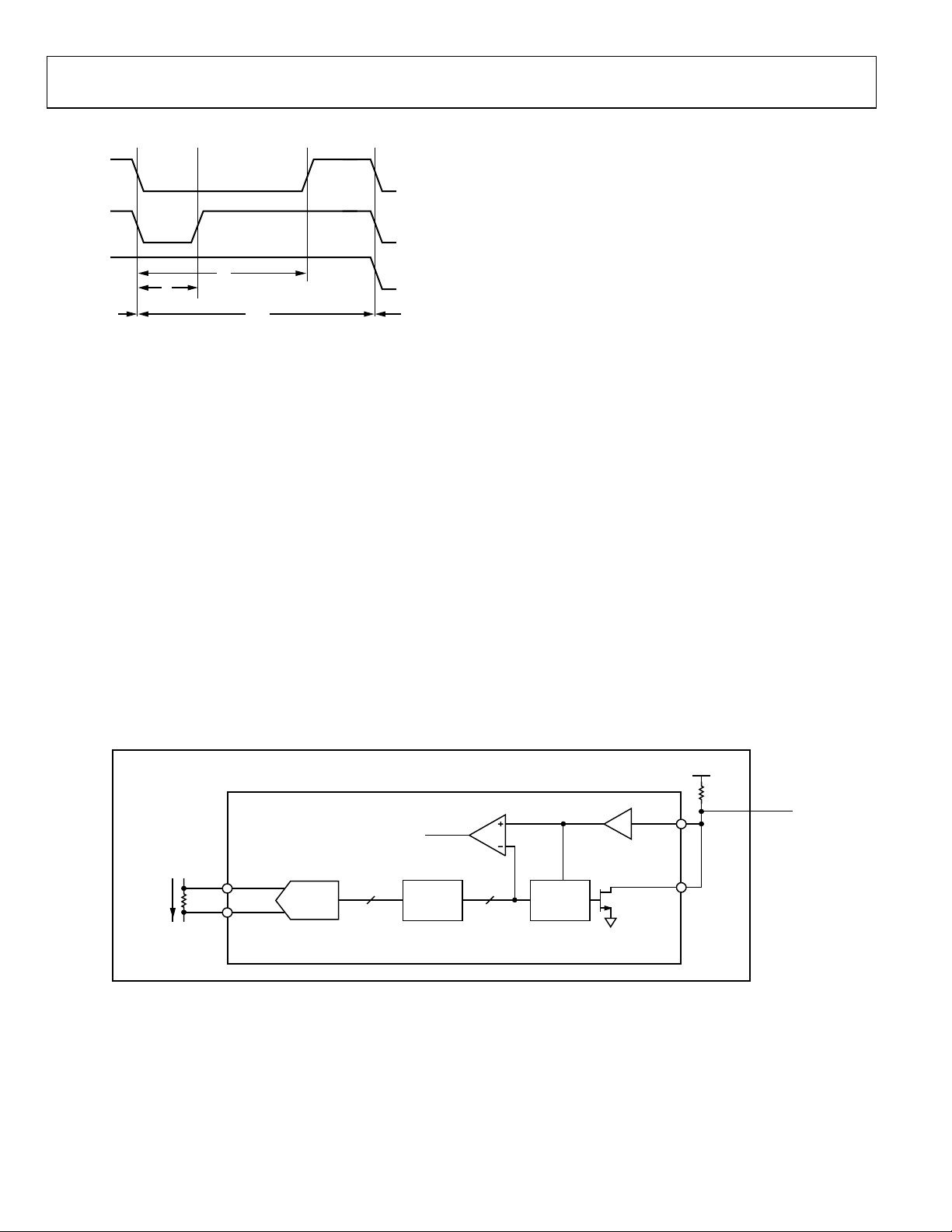
ADP1046 Data Sheet
LOGIC 1
LOGIC 0
IDLE
PREVIOUS
BIT
NEXT
BIT
t
1
t
0
t
BIT
10045-025
CURRENT
SENSE
ADC
1 LSB = 29.3µV
35mV/29.3µV = 1195
MASTER
+
35mV
–
DIGITAL
WORD
DIGITAL
FILTER
÷16
12 BITS
1195 DEC
0x4AB
8 BITS
74 DEC
0x4A
0x4A
SHAREi
CS2+
CS2–
V
DD
SHARE
BUS
8-BIT
WORD
0xB5
8-BIT
WORD
0x4A
SHAREo
I
OUT
= 35A
1mΩ
PSU A
10045-026
Figure 34 shows the possible signals on the share bus.
Figure 34. Share Bus High, Low, and Idle Bits
The length of a bit (t
) is fixed at 10 μs. A Logic 1 is defined as
BIT
a high-to-low transition at the start of the bit and a low-to-high
transition at 75% of t
. A Logic 0 is defined as a high-to-low
BIT
transition at the start of the bit and a low-to-high transition at
25% of t
The bus is idle when it is high during the whole period of t
All other activity on the bus is illegal. Glitches up to t
BIT
.
.
BIT
GLITC H
(200 ns) are ignored.
The digital word that represents the current information is eight
bits long. The ADP1046 takes the eight MSBs of the CS1 or CS2
reading (the current share signal specified in Register 0x29[3])
and uses this reading as the digital word. When read, the share
bus value at any given time is equal to the CS1 or CS2 current
reading (see Figure 35).
Digital Share Bus Scheme
Each power supply compares the digital word that it is outputting
with the digital words of all the other supplies on the bus.
Round 1
In Round 1, every supply first places its MSB on the bus. If a
supply senses that its MSB is the same as the value on the bus, it
continues to Round 2. If a supply senses that its MSB is less than
the value on the bus, it means that this supply must be a slave.
When a supply becomes a slave, it stops communicating on the
share bus because it knows that it is not the master. The supply
then increases its output voltage in an attempt to share more
current.
If two units have the same MSB, they both continue to Round 2
because either of them may be the master.
Round 2
In Round 2, all supplies that are still communicating on the bus
place their second MSB on the share bus. If a supply senses that
its MSB is less than the value on the bus, it means that this supply
must be a slave and it stops communicating on the share bus.
Round 3 to Round 8
The same algorithm is repeated for up to eight rounds to allow
supplies to compare their digital words and, in this way, to
determine whether each unit is the master or a slave.
Digital Share Bus Configuration
The digital share bus can be configured in various ways. The bandwidth of the share bus loop is programmable in Register 0x29[2:0].
The extent to which a slave tries to match the current of the master
is programmable in Register 0x2A[3:0]. The primary side or the
secondary side current can be used as the current share signal
by programming Register 0x29[3].
Figure 35. How the Share Bus Generates the Digital Word to Place on the Digital Share Bus
Rev. A | Page 26 of 96

Data Sheet ADP1046
POWER SUPPLY SYSTEM AND FAULT MONITORING
The ADP1046 has extensive system and fault monitoring
capabilities. The system monitoring functions include voltage,
current, power, and temperature readings. The fault conditions
include out-of-limit values for current, voltage, power, and
temperature. The limits for the fault conditions are programmable.
The ADP1046 has an extensive set of flags that are set when
certain programmed thresholds or limits are exceeded. These
thresholds and limits are described in the Fault Registers section.
FLAGS
The ADP1046 has an extensive set of flags that are set when
certain limits, conditions, and thresholds are exceeded. The
real-time status of these flags can be read in Register 0x00
to Register 0x03. The response to these flags is individually
programmable. Flags can be ignored or used to trigger actions
such as turning off certain PWM outputs or the OrFET gate.
Flags can also be used to turn off the power supply. The ADP1046
can be programmed to respond when these flags are reset. For
more information, see the Fault Registers section.
The ADP1046 also has a set of latched fault registers
(Register 0x04 to Register 0x07). The latched fault registers
have the same flags as Register 0x00 to Register 0x03, but the
flags in the latched registers remain set so that intermittent
faults can be detected. Reading a latched fault register resets
all the flags in that register.
MONITORING FUNCTIONS
The ADP1046 monitors and reports several signals, including
voltages, currents, power, and temperature. All these values are
stored in separate registers and can be read through the I
2
C
interface. For more information, see the Value Registers section.
VOLTAGE READINGS
The VS1, VS2, and VS3 ADCs have an input range of 1.6 V.
The outputs of the ADCs are 12-bit values, which means that
the LSB size is 1.6 V/4096 = 390.625 μV. The user is limited to
an input range of 1.4 V, which means that the ADC output code
is limited to 1.4 V/390.6 μV = 3584.
The equation to calculate the ADC code at a specified voltage
(Vx) at the pin is given by the following formula:
ADC Code = Vx/1.6 × 4096
For example, when there is 1 V on the input of the ADC,
ADC Code = 1 V/1.6 × 4096
ADC Code = 2560
In a 12 V application, the 12 V reading is divided down using
a resistor divider network to provide 1 V at the sense pin.
Therefore, to convert the register value to a real voltage, use
the following formula:
V
= (LSB × 2560) × ((R1 + R2)/R2)
OUT
In a 12 V system, this equates to
V
= (390.625 μV × 2560) × (11 kΩ + 1 kΩ)/1 kΩ
OUT
CURRENT READINGS
CS1 Pin
CS1 has an input range of 1.4 V. The ADC performs a 12-bit
reading conversion of this value, which means that the LSB size
is 1.4 V/4096 = 341.8 μV.
When there is exactly 1 V on the CS1 pin, the value in the CS1
value register (Register 0x13[15:4]) reads 2926.
The equation to calculate the ADC code at a specified CS1
input voltage (Vx) is given by the following formula:
ADC Code = Vx/1.4 × 4096
For example, when there is 1 V on the CS1 input pin,
ADC Code = 1 V/1.4 × 4096
ADC Code = 2926
CS2+, CS2− Pins
The full-scale (FS) range for the CS2 ADC can be set to 60 mV
or 120 mV using Register 0x27[5].
The CS2 ADC has an input range of 120 mV. The resolution is
12 bits, which means that the LSB size is 120 mV/4096 = 29.30 μV.
The user is limited to an input range of 110 mV.
The equation to calculate the ADC code at a specified voltage
(V
) is given by the following formula:
X
ADC Code = Vx/(120 mV) × 4096
For example, when there is 50 mV on the input of the ADC,
ADC Code = 50 mV/120 mV × 4096
ADC Code = 1707
Therefore, to convert the CS2 register value to a real current,
use the following formula:
I
= (CS2_ADC_CODE/4096) × (FS/R
OUT
where:
CS2_ADC_CODE is the value in Register 0x18[15:4].
FS is the full-scale voltage drop (60 mV or 120 mV).
R
is the sense resistor value.
SENSE
For example, if CS2_ADC_CODE = 1520, R
FS = 120 mV, the real current is calculated as follows:
I
= (1520/4096) × (120 mV/10 mΩ)
OUT
= 4.453 A
I
OUT
)
SENSE
= 10 mΩ, and
SENSE
Rev. A | Page 27 of 96
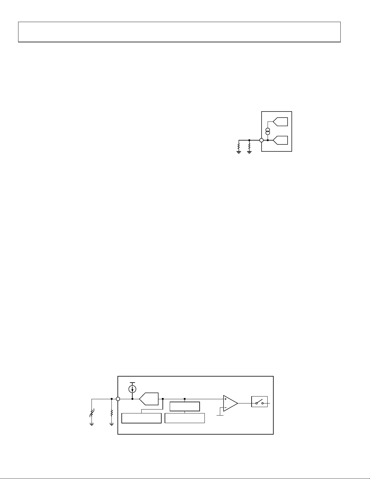
ADP1046 Data Sheet
ADC
DAC
RTD
TH
R
EXT
10045-134
FLAGS
OTP
FLAG
OTP
THRESHOLD
REG 0x2F[7:0]
RTD TEMPERATURE
VALUE REGISTER
REG 0x1A[15:4]
RTD TEMPERATURE
VALUE IN °C
REG 0x1B[7:0]
SIGNAL
CONDITIONING
10µA/20µA/30µA/40µA
RTD
100kΩ
NTC
16.5kΩ
10045-027
RTD
ADC
POWER READINGS
The output power value register (Register 0x19) is the product
of the VS3 voltage value and the CS2 current value. Therefore,
a combination of the formulas in the Voltage Readings section
and the CS2+, CS2− Pins section is used to calculate the power
reading in watts. This register is a 16-bit word. It multiplies two
12-bit numbers and discards the eight LSBs.
P
= V
× I
OUT
OUT
OUT
For example,
P
= 12 V × 4.453 A = 53.436 W
OUT
POWER MONITORING ACCURACY
The ADP1046 power monitoring accuracy is specified relative
to the full-scale range of the signal that it is measuring.
FIRST FLAG FAULT ID AND VALUE REGISTERS
When the ADP1046 registers several fault conditions, it stores
the value of the first fault in a dedicated register. For example,
if the overtemperature (OTP) fault is registered followed by an
OVP fault, the OTP flag is stored in the first flag ID register
(Register 0x10). This register gives the user more information
for fault diagnosis than a simple flag. The contents of this register
are latched, meaning that they are stored until read by the user.
The contents are also reset by toggling PSON. If a flag is set to
be ignored, it does not appear in the first flag register.
EXTERNAL FLAG INPUT (FLAGIN PIN)
The FLAGIN pin can be used to send an external fault signal
into the ADP1046. Register 0x0A[3:0] can be used to program
the FLAGIN flag to trigger an action.
TEMPERATURE READINGS (RTD PIN)
The RTD pin is set up for use with an external negative temperature coefficient (NTC) thermistor. The RTD pin has an internal
programmable current source. An ADC monitors the voltage
on the RTD pin.
The RTD temperature value register, Register 0x1A, is updated
every 10 ms. The ADP1046 stores every ADC sample for 10 ms
and then outputs the average value at the end of the 10 ms period.
The RTD ADC has an input range of 1.6 V and a resolution of
12 bits, which means that the LSB size is 1.6 V/4096 = 390.625 µV.
The user is limited to an input range of 1.3 V, which means that the
maximum ADC output code is limited to 1.3 V/390.6 µV = 3328.
The output of the RTD ADC is linearly proportional to the voltage on the RTD pin. However, thermistors exhibit a nonlinear
function of resistance vs. temperature. Therefore, the user must
perform postprocessing on the RTD ADC reading to accurately
read the temperature.
By connecting an external resistor (R
) in parallel with the
EXT
NTC thermistor (TH), a constant current can be used to
achieve linearization (see Figure 36).
Figure 36. Temperature Measurement Using Thermistor
An internal, precision current source of 10 µA, 20 µA, 30 µA,
or 40 µA can be selected in Register 0x11. This current source
can be trimmed by means of an internal DAC to compensate
for thermistor accuracy (see the RTD/OTP Trim section). The
user can select the output current source using Bits[7:6] of
Register 0x11.
The ADP1046 implements a linearization scheme based on a
preselected combination of external components and current
selection for best performance when measuring linearized
temperatures in degrees Celsius in the industrial range.
For more information about the required thermistor and
selecting and trimming the precision current sources, see
the Temperature Linearization Scheme section.
Optionally, the user can process the RTD reading and perform
postprocessing in the form of a lookup table or polynomial
equation to match the specific NTC thermistor used. With the
internal current source set to 46 µA, the equation to calculate
the ADC code at a specified NTC thermistor value (Rx) is given
by the following formula:
ADC CODE = 46 µA × Rx/1.6 × 4096
For example, at 60°C, the NTC thermistor at the RTD pin is
21.82 kΩ.
RTD_ADC_CODE = 46 µA × 21.82 kΩ/1.6 × 4096 = 2570
Figure 37. RTD Pin Internal Details
Rev. A | Page 28 of 96
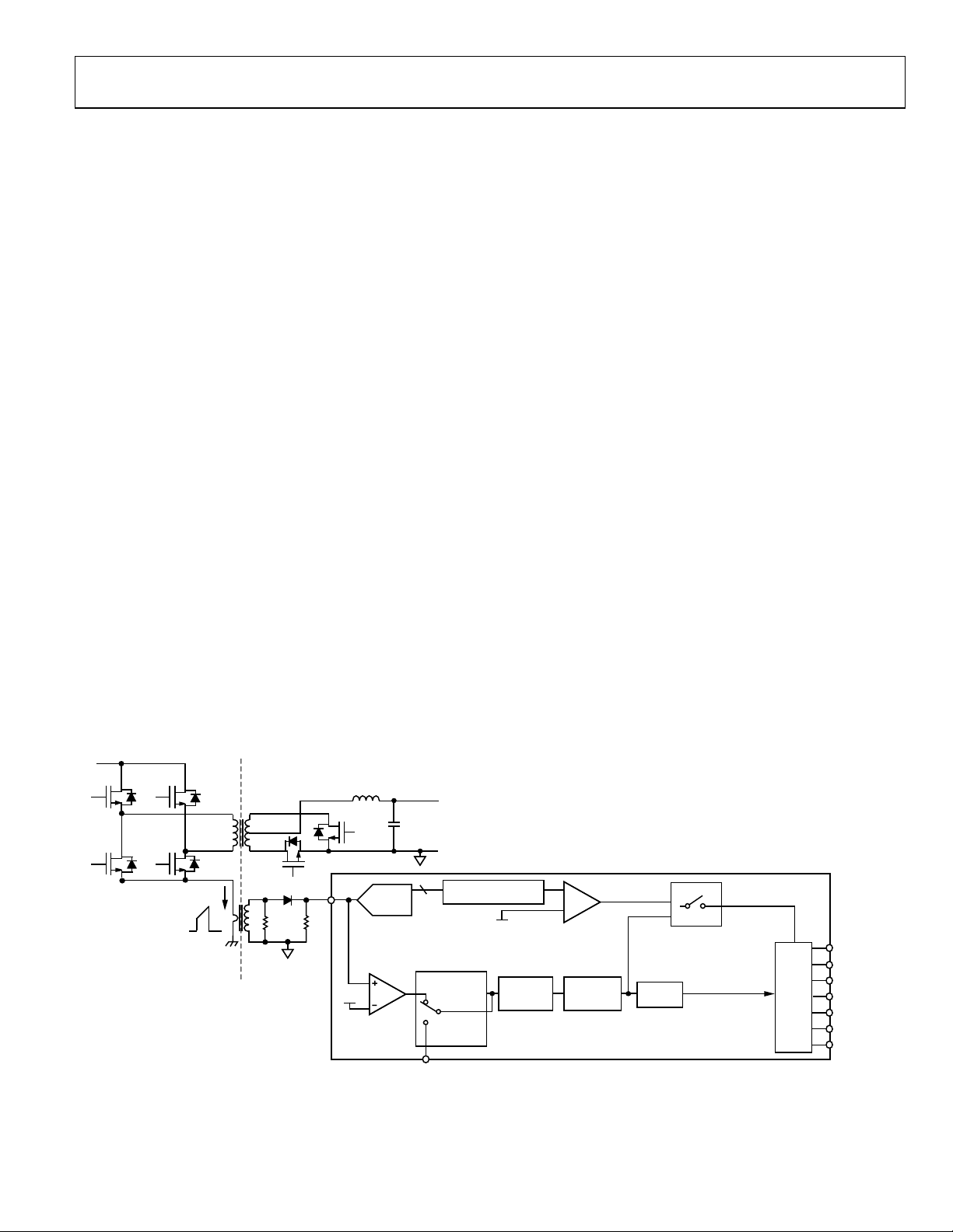
Data Sheet ADP1046
V
IN
OUTA
OUTD
OUTC
OUTB
CS1
CS1
ADC
1.2V
FAST OCP
COMPARATOR
12
CS1 FAST
OCP
FLAG
PWM
CS1 ACCURATE
OCP FLAG
CYCLE-BY-CYCLE
SHUTDOWN
OUTA
OUTB
OUTC
OUTD
SR1
SR2
OUTAUX
FLAGS
CS1
FAST OCP
BYPASS
REG 0x27[4]
CS1
FAST OCP
DEBOUNCE
REG 0x27[7:6]
CS1
FAST OCP
BLANKING
REG 0x22[7:5]
FLAGIN
CS1 ACCURATE
OCP SETTING
REG 0x22[4:0]
SHUTDOWN
CYCLE
TIMEOUT
REG 0x27[1:0]
ASYNCHRONOUS
2.62ms AVERAGING
10045-135
Temperature Linearization Scheme
The ADP1046 implements a linearization scheme based on a
preselected combination of thermistor (100 kΩ, 1%), external
resistor (16.5 kΩ, 1%), and the 46 µA current source for best
performance when linearizing measured temperatures in the
industrial range.
The required NTC thermistor should have a resistance of
100 kΩ, 1%, such as the NCP15WF104F03RC (beta = 4250,
1%). It is recommended that 1% tolerance be used for both the
resistor and beta values.
Reading the Linearized Temperature
Reading Register 0x1B (updated every 10 ms) returns the current
temperature according to an internal linearization scheme. See
Table 1 for the specified accuracy of these measurements. The
temperature reading result is represented in 8-bit decimal format
in °C; therefore, the temperature range for this reading is from
0°C to 255°C.
OVERTEMPERATURE PROTECTION (OTP)
If the temperature sensed at the RTD pin exceeds the threshold
programmed in Register 0x2F, the OTP flag is set. The response
to the OTP flag is programmable using Register 0x0B[7:4].
An RTD trim is required to make accurate temperature readings
at the lower end of the RTD ADC range to account for tolerances
in the NTC thermistor and the external resistor. This trim results
in a more accurate measurement for determining the OTP
threshold (see the RTD/OTP Trim section).
OVERCURRENT PROTECTION (OCP)
The ADP1046 has several OCP functions. CS1 and CS2± have
separate OCP circuits to provide both primary and secondary
side protection.
CS1 OCP
CS1 has two protection circuits: CS1 fast OCP and CS1 accurate
OCP (see Figure 38).
CS1 Fast OCP
CS1 fast OCP is an analog comparator. When the voltage at the
CS1 pin exceeds the (fixed) 1.2 V threshold, the CS1 fast OCP
flag is set. A programmable blanking time can be set to ignore
the leading edge current spike at the beginning of the current
signal (leading edge blanking).
A debounce time can be programmed to improve the noise immunity of the OCP circuit. When the CS1 fast OCP comparator is
set, the OUTA, OUTB, OUTC, and OUTD PWM outputs are
immediately disabled for the remainder of the switching cycle.
These outputs are reenabled at the start of the next switching
cycle. This function cannot be bypassed.
CS1 Accurate OCP
CS1 accurate OCP is used for more precise control of overcurrent
protection. With CS1 accurate OCP, the reading at the output of
the CS1 ADC (Register 0x13) is compared to a programmable
OCP limit. The CS1 accurate OCP value can be programmed
from 0 to 31 decimal using Register 0x22[4:0]. If the CS1 reading
exceeds the CS1 accurate OCP limit, the CS1 accurate OCP flag
is set. The CS1 ADC is asynchronously sampled, and the readings
are averaged every 2.62 ms to make a fault decision. The flag
response is programmed in Register 0x08.
Figure 38. CS1 OCP Detailed Internal Schematic
Rev. A | Page 29 of 96

ADP1046 Data Sheet
CS2 ACCURATE
OCP SETTING
REG 0x26
CS2– CS2+
5kΩ 5kΩ
ADC
12
ASYNCHRONOUS
2.62ms AVERAGI NG
PROGRAMMABLE DEBOUNCE
AND ACTION
(REG 0x0E AND REG 0x09)
1V
200µA200µA
10045-136
OCP
V
OUT
V
OUT
NOMINAL
I
OUT
0.97 × OCP
10045-137
Figure 39. CS2 OCP Detailed Internal Schematic
CS2 OCP
CS2 has one OCP protection circuit: CS2 accurate OCP (see
Figure 39). The reading at the output of the CS2 ADC (Register
0x18) is compared to a programmable OCP threshold. The CS2
OCP threshold can be programmed using Register 0x26[7:0]. If
the CS2 reading exceeds the CS2 OCP threshold, the CS2 accurate
OCP flag is set. The CS2 ADC is asynchronously sampled, and
the readings are averaged every 2.62 ms to make a fault decision.
The flag response is programmed in Register 0x09.
CONSTANT CURRENT MODE
The ADP1046 can be configured to operate in constant current
mode. The threshold to enter constant current mode operation is
3% current below the CS2 accurate OCP setting (see Figure 40).
Below this current, the part operates in constant voltage mode,
using the output voltage as the feedback signal for closed-loop
operation.
vs. I
Figure 40. Constant Current Mode (V
OUT
When the ADP1046 reaches the constant current mode threshold,
a flag is set in Register 0x02[4] and in Register 0x06[4] (real-time
and latched flag registers, respectively). When this flag is set,
the CS2 current reading is used to control the output voltage
regulation point. The output voltage is ramped down linearly as
the load increases to ensure that the current remains constant.
OUT
)
The constant current control loop is relatively low bandwidth
because the current is averaged over a 328 µs period. The output
voltage changes at a maximum rate of 1.18 V/sec at the VS3± pins;
therefore, the instantaneous value of the current can exceed the
constant current limit for a very short period of time, depending upon the transient.
As the output voltage falls, the UVP flag (Register 0x0B[3:0])
can be used to program a shutdown action.
OVERVOLTAGE PROTECTION (OVP)
The ADP1046 has three separate OVP circuits. If the output
voltage at the VS1 pin, VS2 pin, or VS3± pins exceeds the
programmable threshold for that pin, the appropriate OVP flag
is set. The flag response is programmed in Register 0x09[3:0]
for the VS2 and VS3 OVP flags or in Register 0x0A[7:4] for the
VS1 OVP flag.
VS1 has two OVP circuits: a fast comparator (fast OVP) and an
ADC based comparator (accurate OVP). VS2 and VS3 share an
accurate OVP circuit.
The OVP circuits can be programmed for different OVP
thresholds. See Register 0x32 and Register 0x33 for more
information.
The sampling time for the ADC based comparators is 80 µs.
Additional debounce in steps of 80 µs can be added using
Bits[1:0] of Register 0x32 and Register 0x33.
The fast OVP comparator also has a programmable threshold and
debounce time. These values are programmed in Register 0x37.
Rev. A | Page 30 of 96

Data Sheet ADP1046
UNDERVOLTAGE PROTECTION (UVP)
If the voltage sensed at the VS1 pin falls below the programmable UVP threshold, the UVP flag is set. The UVP threshold
is programmed in Register 0x34; the GUI can also be used, as
shown in Figure 41.
The response to the UVP flag is programmable in Register
0x0B[3:0]. Undervoltage protection and the UVP flag are
disabled during soft start.
AC SENSE (ACSNS)
The ACSNS circuit performs multiple monitoring and control
functions. Two ADCs and a fast comparator are connected to
this pin.
The fast ADC is used for the voltage feedforward function
(see the Voltage Line Feedforward and ACSNS section).
This ADC has an equivalent resolution of 11 bits at 10 μs.
The slow ADC is used to report the input voltage. This
ADC has a resolution of 12 bits at 10 ms.
The fast comparator is used to monitor whether a
switching waveform is present at the output of the
synchronous rectifier stage (or rectifier diodes).
The pick-off point upstream of the output inductor is connected
to the ACSNS pin through an external RCD divider network.
The output of the ACSNS slow ADC is a 12-bit value reported
in Register 0x14. The gain of this ADC can be adjusted using
Register 0x5E[6:0] to compensate for divider errors and the
voltage spike.
The equation to calculate the ADC code is given by the
following formula:
ADC Code = Vx/1.6 × 4096
where Vx is the voltage at the ACSNS pin.
For example, when there is 1 V on the input of the ADC
ADC Code = 1 V/1.6 × 4096
ADC Code = 2560
= (Vx) × (R1 + R2)/R2
V
SENSE
where V
is the filtered secondary voltage.
SENSE
The primary input voltage can be calculated by multiplying
by the turns ratio (N1/N2) as follows:
V
SENSE
V
= Vx × (R1 + R2)/R2 × (N1/N2)
PRIMARY
The ACSNS comparator threshold is set at 0.45 V. If the average
voltage on the ACSNS pin falls below this threshold, the ACSNS
flag is set in Register 0x03[2] and in Register 0x07[2] (real-time
and latched flag registers, respectively), and the programmed
action for the flag is executed.
When operating in resonant mode, the ACSNS comparator is
used for the timing of the synchronous rectifiers and, therefore,
the additional features of the ADC cannot be used. For more
information, see the Resonant Mode Operation section.
10045-138
Figure 41. Voltage Sense Window in Simulation Mode (ADP1046 GUI)
Rev. A | Page 31 of 96

ADP1046 Data Sheet
100
90
91
92
93
94
95
96
97
98
99
0 20 40 60 80 100 12010 30 50 70 90 110
V
OUT
(%)
R
SENSE
VOLTAGE DROP (mV)
10045-030
SETTING 7
SETTING 6
SETTING 5
SETTING 4
SETTING 3
SETTING 2
SETTING 1
SETTING 0
100
88
90
92
94
96
98
0 10 20 30 40 50 605 15 25 35 45 55
V
OUT
(%)
R
SENSE
VOLTAGE DROP (mV)
10045-031
SETTING 7
SETTING 6
SETTING 5
SETTING 4
SETTING 3
SETTING 2
SETTING 1
SETTING 0
VOLT-SECOND BALANCE
The ADP1046 has a dedicated circuit to maintain volt-second
balance in the main transformer when operating in full-bridge
topology. This circuit eliminates the need for a dc blocking capacitor. In interleaved topologies, volt-second balance can also be
used for current balancing to ensure that each interleaved phase
contributes equal power.
The circuit monitors the current flowing in both legs of the fullbridge topology and stores this information. It compensates the
selected PWM signals to ensure equal current flow in both legs
of the full-bridge topology. The input is through the CS1 pin.
Several switching cycles are required for the circuit to operate
effectively. The maximum amount of modulation applied to
each edge of the selected PWM outputs is programmable to
±80 ns or ±160 ns in Register 0x28[2].
The volt-second balance settings are programmed in Register 0x28
and in Register 0x76 through Register 0x78. It is recommended
that the Analog Devices software GUI be used to program these
settings.
The compensation of the PWM drive signals is performed on
the edges of two selected outputs. The SR1 and SR2 edges can
also be independently set to modulate due to the volt-second
balance circuit to maintain the timing relation to the primary
side signals.
DIGITAL LOAD LINE AND SLEW RATE
The ADP1046 can optionally introduce a digital load line into
the power supply. This option is programmed in the load line
impedance register (Register 0x36). Two parameters can be
configured independently: slew rate and load line value.
The slew rate (Register 0x36[6:4]) determines how quickly the
output voltage is adjusted in response to a change in the digital
reference. Eight different settings are available.
The load line value (Register 0x36[2:0]) controls the slope of
the load line. The amount of output resistance introduced can
be calculated as follows:
R
= 0.1 × V
OUT
where:
V
CS2 R
is the nominal output voltage when VS3 = 1 V.
OUT_NOM
is the sense resistor value.
SENSE
CS2 Range is 120 mV or 60 mV.
LOAD_SET[2:0] is the value of Bits[2:0] in Register 0x36
(0 to 7 decimal).
OUT_NOM
× CS2 R
/(CS2 Range × 2
SENSE
LOAD_SET[2:0]
)
Rev. A | Page 32 of 96
For example, if V
OUT_NOM
= 12 V, CS2 R
= 10 mΩ,
SENSE
CS2 Range = 120 mV, and LOAD_SET[2:0] = 3,
R
= 0.1 × 12 V × 10 mΩ/(120 mV × 23) = 12.5 mΩ
OUT
This feature can be used for advanced current sharing techniques.
By default, the load line is disabled. The load line is introduced
digitally by modifying the value of the digital reference based
on the CS2 reading.
Figure 42 and Figure 43 show the load line as a percentage of
V
vs. the R
OUT
voltage drop.
SENSE
Figure 42. Load Line Settings with 120 mV CS2 Range
Figure 43. Load Line Settings with 60 mV CS2 Range

Data Sheet ADP1046
POWER SUPPLY CALIBRATION AND TRIM
The ADP1046 allows the entire power supply to be calibrated
and trimmed digitally in the production environment. It can
calibrate items such as output voltage and trim for tolerance
errors introduced by sense resistors and resistor dividers, as well
as its own internal circuitry. The part is factory trimmed, but it
can be retrimmed by the user to compensate for the errors introduced by external components. The ADP1046 GUI allows the
user to automatically revert the trim settings to their factory
default values.
To un lo c k the trim registers for write access, write to the
TRIM_PASSWORD register (Register 0x89). Write the
trim password twice (the factory default password is 0xFF).
The ADP1046 allows the user enough trim capability to trim
for external components with a tolerance of 0.5% or better. If
the ADP1046 is not trimmed in the production environment,
it is recommended that components with a tolerance of 0.1% or
better be used for the inputs to CS1, CS2, VS1, VS2, and VS3 to
meet data sheet specifications.
CS1 TRIM
Using a DC Signal
A known voltage (Vx) is applied at the CS1 pin. The CS1 ADC
should output a digital code equal to Vx/1.4 × 4096. The CS1
gain trim register (Register 0x21) is adjusted until the CS1 ADC
value in Register 0x13[15:4] reads the correct digital code.
Using an AC Signal
A known current (Ix) is applied to the PSU input. This current
passes through a current transformer, a diode rectifier, and an
external resistor (R
) to convert the current information to a
CS1
voltage (Vx). This voltage is fed into the CS1 pin. The voltage
(Vx) is calculated as follows:
Vx = Ix × (N1/N2) × R
CS1
where N1/N2 is the turns ratio of the current transformer.
The CS1 ADC outputs a digital code equal to Vx/1.4 × 4096. The
CS1 gain trim register (Register 0x21) is adjusted until the CS1
ADC value in Register 0x13[15:4] reads the correct digital code.
CS2 TRIM
The CS2 trim must compensate for offset and gain errors. The
offset error requires both an analog trim and a digital trim. This
error includes the mismatch of the level shifting resistors to the
inputs of the CS2± differential amplifier and the tolerance of the
current sense element.
CS2 Offset Trim
Offset errors can be introduced by the external level shifting
resistors and the internal current sources. It is best to use two
0.1% matched resistors or matched resistors within the same
package.
It is important to perform the CS2 offset trim as described
in the following steps:
1. Set high-side or low-side current sensing using
Register 0x27[2].
2. Set the nominal full-scale sense resistor voltage drop in
Register 0x27[5] to 1 for the 120 mV range or to 0 for the
60 mV range.
3. Apply no-load current across the sense resistor.
4. Set the CS2 gain trim value to 0 (Register 0x23 = 0).
5. Set the CS2 digital offset trim value to 0 (Register 0x25 = 0).
6. Adjust the CS2 analog offset trim value in Register 0x24[6:0].
For the 120 mV range, adjust Register 0x24 until the CS2
value in Register 0x18[15:4] reads as close to 100 decimal
(0x64) as possible; this value must be greater than 50 (0x32).
For the 60 mV range, adjust Register 0x24 until the CS2
value in Register 0x18[15:4] reads as close to 200 decimal
(0xC8) as possible; this value must be greater than 100 (0x64).
7. Adjust the CS2 digital offset trim value in Register 0x25
until the CS2 value in Register 0x18[15:4] reads 0.
The offset trim is now completed, and the ADC code reads 0 if
there is a no-load current across the sense resistor.
CS2 Gain Trim
After performing the offset trim, perform the gain trim to
remove any mismatch that is introduced by the sense resistor
tolerance. The ADP1046 can trim for sense resistors with a
tolerance of 1% or better.
1. Apply a known load current (I
) across the sense resistor.
OUT
2. Adjust the CS2 gain trim value in Register 0x23[5:0] until
the CS2 value in Register 0x18[15:4] reads the value
calculated by the following formula:
CS2 Value = I
OUT
× R
/FS × 4096
SENSE
where:
FS is the full-scale voltage drop (120 mV or 60 mV).
R
is the sense resistor value.
SENSE
If CS2 is programmed to the 120 mV range and I
R
= 10 mΩ, and FS = 120 mV,
SENSE
= 10 A,
OUT
CS2 Value = (10 A × 10 mΩ)/120 mV × 4096
CS2 Value = 3413 decimal
If CS2 is programmed to the 60 mV range and I
R
= 5 mΩ, and FS = 60 mV,
SENSE
OUT
= 5 A,
CS2 Value = (5 A × 5 mΩ)/60 mV × 4096
CS2 Value = 1707 decimal
The CS2 circuit is now trimmed. The OCP limits and settings
should be configured after the current sense trim is performed.
Rev. A | Page 33 of 96

ADP1046 Data Sheet
VOLTAGE CALIBRATION AND TRIM
The voltage sense inputs are optimized for sensing signals at
1 V (the usable input range is 1.4 V). In a 12 V system, a 12:1
resistor divider is required to reduce the 12 V signal to below
1.4 V. It is recommended that the output voltage of the power
supply be reduced to 1 V at this pin for best performance. The
tolerance of the resistor divider introduces errors that need to
be trimmed. The ADP1046 has enough trim range to trim out
errors introduced by resistors with a tolerance of 0.5% or better.
The VS1, VS2, and VS3 ADCs produce a digital code equal to
VSx/1.6 × 4096. The ADCs output a digital word of 2560
decimal (0xA00) in Bits[15:4] of Register 0x15, Register 0x16,
and Register 0x17 when there is exactly 1 V at their inputs.
OUTPUT VOLTAGE SETTING (VS3+, VS3− TRIM)
The VS3± inputs require a gain trim. Set the output regulation
point to 100% of the nominal value (Register 0x31 = 0xA0).
Enable the power supply with no-load current. The power
supply output voltage is divided down by the VS3 resistor
divider to give 1 V across the VS3+ and VS3− differential input
pins. The VS3 trim register (Register 0x3A) is adjusted until
the output voltage is at the desired value. This step should be
performed before any other trim routine. The VS3 voltage
value in Register 0x17[15:4] reads 2560 decimal (0xA00).
VS1 TRIM
The VS1 input requires a gain trim. Enable the power supply
with no-load current. It is recommended that the VS1 voltage
be divided down by the VS1 resistor divider to give 1 V at the
VS1 pin. The VS1 trim register (Register 0x38) is adjusted until
the VS1 value in Register 0x15[15:4] reads 2560 decimal (0xA00).
VS2 TRIM
The VS2 input requires a gain trim. Enable the power supply
with no-load current. It is recommended that the VS2 voltage
be divided down by the VS2 resistor divider to give 1 V at the
VS2 pin. The VS2 trim register (Register 0x39) is adjusted until
the VS2 value in Register 0x16[15:4] reads 2560 decimal (0xA00).
RTD/OTP TRIM
The RTD input requires two trims: one for the current source
and one for the ADC. To use the internal linearization scheme,
additional trimming procedures are required.
Rev. A | Page 34 of 96
Trimming the Current Source
Bits[7:6] of Register 0x11 set the value of the current source to
10 µA, 20 µA, 30 µA, or 40 µA. Bits[5:0] of Register 0x11 can be
used to fine-tune the current value. By fine-tuning the internal
current source, component tolerance can be compensated for
and errors can be minimized. One LSB in Bits[5:0] = 160 nA.
A decimal value of 1 adds 160 nA to the current source set by
Bits[7:6]; a decimal value of 63 adds 63 × 160 nA = 10.08 µA
to the current source set by Bits[7:6].
To program a value for the current source, select the nearest
possible option (10 µA, 20 µA, 30 µA, or 40 µA) using
Register 0x11[7:6]. Then use Register 0x11[5:0] to achieve
the finer step size.
For example, to use a value of 46 µA as the current source,
follow these steps:
1. Place a known resistor (Rx) from RTD to AGND.
2. Set Register 0x11[7:6] to 11 (40 µA).
3. Increase the value of Register 0x11[5:0] one LSB at a time
until the voltage at the RTD pin is V
The current source is now calibrated and is set to the factory
default value.
= 46 µA × Rx.
RTD
Trimming the ADC
Due to the nonlinear nature of the thermistor, two trimming
options can be used.
Using the Internal Linearization Scheme
The first option uses the internal linearization scheme with
46 µA RTD current, which provides an accurate reading in °C
read in Register 0x1B in decimal format.
A 100 kΩ, 1% NTC thermistor with beta = 4250, 1% (such as the
NCP15WF104F03RC) in parallel with an external resistor of
16.5 kΩ, 1%, should be used with the ADP1046. With this NTC
thermistor and resistor combination, the ADP1046 default current
source trim is set to 46 µA to achieve the best possible accuracy
over temperatures ranging from 85°C to 125°C.
If an external microcontroller is used, the RTD ADC code in
Register 0x1A can be fed into the microcontroller and a different
linearization scheme can be implemented in terms of a best-fit
polynomial for the selected NTC characteristics.

Data Sheet ADP1046
A
Using the OTP Value
The second option does not use the linearization scheme.
Instead, the user programs an RTD current and sets the OTP
threshold in millivolts. Due to the nonlinear nature of the NTC
thermistor, it is best to use a resistor in parallel with the NTC
thermistor to aid in the linearization of the voltage seen at the
RTD pin.
This procedure trims out the errors/tolerances in the NTC thermistor and the external resistor. Calculation of the parallel resistor
can be done by knowing the NTC resistance characteristic across
various temperatures.
To use this procedure, the temperatures and equivalent resistances
of the NTC thermistor and parallel resistor combination must
be known.
In Figure 44, T2 is the OTP threshold that sets the OTP flag,
and T1 is the temperature at which the OTP flag is cleared.
DC CODE
V2 V1
Figure 44. RTD Pin Voltage, ADC Code, and Temperature
RTD PIN
VOLTAGE
RTD PIN VOL T AGE
V1
V2
T1 T2
TEMPERATURE
The following procedure should be used:
1. Adjust the desired RTD current source, I
, as described
RTD
in the Trimming the Current Source section.
2. Set the temperature to the OTP threshold.
3. Adjust the offset trim registers (Register 0x1C and Register
0x20) until the reading in Register 0x1A is the same as V2
(in mV).
4. Set the OTP threshold (Register 0x2F) to the value of V2.
5. Set the temperature to the hysteresis point where the OTP
flag is cleared.
6. Adjust the temperature gain trim register (Register 0x2B)
until the correct voltage is seen in Register 0x1A.
10045-300
The ADC is now trimmed and is linear between the two
temperatures of interest.
This procedure achieves the most accurate OTP because it takes
into account the part-to-part variations of the ADP1046 and the
tolerances of the thermistor being used.
ACSNS CALIBRATION AND TRIM
The ACSNS feedforward ADC (see Figure 18) is used for
voltage line feedforward and cannot be trimmed by the user.
The ACSNS slow ADC requires a gain trim. Enable the power
supply with full load current at the nominal input voltage. The
secondary peak reverse voltage on the output rectifiers is
filtered by an external RCD circuit (see Figure 18).
To trim the ACSNS ADC, the user can reverse-calculate the
primary voltage as follows:
V
= Vx × (R1 + R2)/R2 × (N1/N2)
PRIMARY
where:
Vx is the voltage at the ACSNS pin.
N1/N2 is the turns ratio.
The ACSNS gain trim register (Register 0x5E) is adjusted until
this calculated voltage is equal to the desired primary input
voltage.
Another way to trim the ACSNS ADC uses the average secondary voltage. With known values for the nominal input voltage,
transformer turns ratio, and resistor dividers at the ACSNS pin,
the ACSNS gain trim register (Register 0x5E) is adjusted to give
code 2560 decimal (0xA00).
ADC Code = Vx/1.6 × 4096
where Vx is the voltage at the ACSNS pin.
The resistors in Figure 18 are sized such that the first time
constant, RC, is long enough to prevent overcharging of the
capacitor (roughly 200 ns in a typical application), whereas the
second time constant, (R1 + R2) × C, is long enough to keep the
average voltage constant during the rectifier off time.
Rev. A | Page 35 of 96

ADP1046 Data Sheet
LAYOUT GUIDELINES
This section explains best practices that should be followed
to ensure optimal performance of the ADP1046. In general,
all components should be placed as close to the ADP1046 as
possible. All signals should be referenced to their respective
grounds.
CS2+ AND CS2−
The routing of the traces from the sense resistor to the ADP1046
should be laid out in parallel to each other. The traces should
also be kept close together and as far from the switch nodes as
possible.
VS3+ AND VS3−
The routing of the traces from the remote voltage sense point
to the ADP1046 should be laid out in parallel to each other.
The traces should also be kept close together and as far from
the switch nodes as possible. Place a 100 nF capacitor from VS3−
to AGND to reduce common-mode noise.
VDD
Place decoupling capacitors as close to the part as possible.
A 4.7 µF capacitor from VDD to AGND is recommended.
SDA AND SCL
The routing of the traces should be laid out in parallel to each
other. The traces should also be kept close together and as far
from the switch nodes as possible.
CS1
Run the traces from the current sense transformer to the
ADP1046 in parallel to each other. The traces should also be
kept close together and as far from the switch nodes as possible.
EXPOSED PAD
The exposed pad underneath the ADP1046 should be soldered
to the PCB AGND plane.
VCORE
Place a 330 nF decoupling capacitor from this pin to DGND as
close to the part as possible.
RES
Place a 10 kΩ, ±0.1% resistor from this pin to AGND as close to
the part as possible.
RTD
Route a single trace to the ADP1046 from the thermistor using
a dedicated trace to AGND. Place the thermistor close to the
hottest part of the power supply.
AGND, DGND, AND PGND
Create an AGND ground plane and make a single-point (star)
connection to the power supply system ground. Connect DGND
to AGND with a very short trace using a star connection.
Connect PGND to AGND using a star connection.
Rev. A | Page 36 of 96

Data Sheet ADP1046
I2C INTERFACE COMMUNICATION
The ADP1046 I2C slave is a 2-wire interface that can be used
to communicate with other I
2
C-compliant master devices and
is compatible in a multimaster, multislave bus configuration.
FEATURES
The function of the I2C slave is to decode the command sent from
the master device and respond as requested. Communication is
established using a 2-wire interface with a clock line (SCL) and
data line (SDA). The I
2
C slave is designed to externally move
chunks of 8-bit data (bytes) while maintaining compliance with
2
the I
C protocol, based on the Philips I2C Bus Specification,
Version 2.1, dated January 2000. The I
2
C protocol incorporates
the following features:
Slave operation on multiple device systems
7-bit addressing
100 kB/sec and 400 kB/sec data rates
General call address support
Support for clock low extension (clock stretching)
Separate multiple byte receive and transmit FIFO
Extensive communication fault monitoring
OVERVIEW
The I2C slave module is a 2-wire interface that can be used to
communicate with other I
fer protocol is based on the Philips I
ADP1046 is always configured as a slave device in the overall
system. The ADP1046 communicates with the master device
using one data pin (SDA) and one clock pin (SCL). Because the
ADP1046 is a slave device, it cannot generate the clock signal.
However, it is capable of stretching the SCL line to put the
master device in a wait state when it is not ready to respond
to the master’s request.
Communication is initiated when the master device sends a
command to the I
write commands, in which case data is transferred between the
devices in a byte-wide format. Commands can also be send
commands, in which case the command is executed by the slave
device upon receiving the stop bit. The stop bit is the last bit in
a complete data transfer, as defined in the I
protocol. During communication, the master and slave devices
send acknowledge (A) or no acknowledge (NA) bits as a method
of handshaking between devices. Refer to the Philips I
Specification, Version 2.1, dated January 2000, for a more detailed
description of the communication protocol.
2
C-compliant master devices. Its trans-
2
C slave device. Commands can be read or
2
C transfer mechanism. The
2
C communication
2
C Bus
I2C ADDRESS
The I2C address of the ADP1046 is set by connecting an
external resistor from the ADD pin to AGND. Table 6 lists the
recommended resistor values and the associated I
2
C addresses.
Seven different addresses can be used.
The recommended resistor values in Table 6 must be 1%
tolerance resistors.
2
Table 6. Recommended Resistor Values for I
C Addresses
I2C Address Resistor Value (kΩ)
0x50 10 (or connect the ADD pin directly to AGND)
0x51 28.7
0x52 48.7
0x53 68.1
0x54 88.7
0x55 109
0x57 200 (or connect the ADD pin directly to VDD)
DATA TRANSFER
Format Overview
The I2C slave follows the transfer protocol of the Philips I2C Bus
Specification. Data transfers are byte-wide, lower byte first. Each
byte is transmitted serially, most significant bit (MSB) first. A
typical transfer is shown in Figure 45.
7-BIT SLAVE
S
ADDRESS
= MASTER-TO-SLAVE
= SLAVE-TO-MASTER
W A A ... P
Figure 45. Basic Data Transfer
Figure 45 to Figure 52 use the following abbreviations:
S = start condition
Sr = repeated start condition
P = stop condition
R = read bit
W
= write bit
A = acknowledge bit (0)
NA = no acknowledge bit (1)
Refer to the I
2
C specification for an in-depth discussion of the
transfer protocols.
8-BIT
DATA
10045-140
Rev. A | Page 37 of 96

ADP1046 Data Sheet
S
7-BIT SLAVE
ADDRESS
W A
A
PCOMMAND CODE
= MASTER- TO-SLAVE
= SLAVE-TO-MASTER
10045-141
S
7-BIT SLAVE
ADDRESS
W A
A A
P
COMMAND
CODE
DATA
BYTE
= MASTER- TO-SLAVE
= SLAVE-TO-MASTER
10045-142
S
7-BIT SLAVE
ADDRESS
W
A
A
DATA
BYTE
HIGH
COMMAND
CODE
DATA
BYTE
LOW
A
A
P
= MASTER- TO-SLAVE
= SLAVE-TO-MASTER
10045-143
DATA BYTE NA P
S
7-BIT SLAVE
ADDRESS
W
A A
7-BIT SLAVE
ADDRESS
COMMAND
CODE
Sr R A
= MASTER- TO-SLAVE
= SLAVE-TO-MASTER
10045-144
DATA BYTE LOW A
NA PDATA BYTE HIGH
S
7-BIT SLAVE
ADDRESS
W
A A
7-BIT SLAVE
ADDRESS
COMMAND
CODE
Sr R A
= MASTER- TO-SLAVE
= SLAVE-TO-MASTER
10045-145
DATA BYTE 1 A ... A
PDATA BYTE N
S
7-BIT SLAVE
ADDRESS
W A A
BYTE
COUNT = N
COMMAND
CODE
A
= MASTER- TO-SLAVE
= SLAVE-TO-MASTER
10045-146
S
7-BIT SLAVE
ADDRESS
7-BIT SLAVE
ADDRESS
W
A
A
COMMAND
CODE
ARSr
DATA
BYTE 1
A
A
... NA
DATA
BYTE N
P
BYTE
COUNT = N
= MASTER- TO-SLAVE
= SLAVE-TO-MASTER
10045-147
SCL
SDA
START STOP
10045-148
Command Overview
Data transfer using the I2C slave is established using commands.
W
All commands start with a slave address with the R/
(set to 0), followed by the command code (register address). All
commands supported by the ADP1046 follow one of the protocol
types shown in Figure 46 to Figure 52.
bit cleared
Figure 46. Send Byte Protocol
Figure 47. Write Byte Protocol
Figure 48. Write Word Protocol
Figure 49. Read Byte Protocol
Figure 50. Read Word Protocol
Figure 52. Block Read Protocol
Clock Generation and Stretching
The ADP1046 is always a slave in the overall system; therefore,
the device never needs to generate the clock, which is done by
capable of clock stretching to put the master in a wait state. By
the master device in the system. However, the I
2
C slave device is
stretching the SCL signal during the low period, the slave device
communicates to the master device that it is not ready and that
the master device must wait.
Conditions where the I
2
C slave device stretches the SCL line low
include the following:
• The master device is transmitting at a higher baud rate
than the slave device.
• The receive FIFO buffer of the slave device is full and must
be read before continuing. This prevents a data overflow
condition.
• The slave device is not ready to send data that the master
has requested.
Note that the slave device can stretch the SCL line only during
the low period. Also, whereas the I
stretching of the SCL line, the ADP1046 limits the maximum
2
C specification allows indefinite
time that the SCL line can be stretched, or held low. For more
information about the maximum time, see the Timeout
Condition section.
Start and Stop Conditions
Start and stop conditions involve serial data transitions while the
serial clock is at a logic high level. The I
2
C slave device monitors
the SDA and SCL lines to detect the start and stop conditions
and transition its internal state machine accordingly. Typical
start and stop conditions are shown in Figure 53.
Figure 51. Block Write Protocol
Figure 53. Start and Stop Transitions
Rev. A | Page 38 of 96

Data Sheet ADP1046
GENERAL CALL SUPPORT
The ADP1046 is capable of decoding and acknowledging a
general call address. The general call address is supported for
send, write, and read commands that use Address 0x00 as the
slave address. The I
2
C slave responds to both its own address
and to the general call address (0x00).
Note that all commands start with a slave address with the R/
W
bit cleared (set to 0), followed by the command code. This is
also true when using the general call address to communicate
with the I
2
C slave device.
10-BIT ADDRESSING
The ADP1046 does not support 10-bit addressing as defined in
2
the I
C specification.
FAST MODE
Fast mode (400 kB/sec) uses essentially the same mechanics
as the standard mode of operation; the electrical specifications
and timing are most affected. The I
2
C slave is capable of communicating with a master device operating in standard mode
(100 kB/sec) or fast mode.
REPEATED START CONDITION
In general, a repeated start condition is the absence of a stop
condition between two transfers. The two transfers can be of
any direction type, for example, a transmit followed by a receive
or a receive followed by a transmit. However, the ADP1046 I
2
C
communication protocol uses the repeated start condition only
when performing a read access (read byte, read word, and block
read). Other uses of the repeated start condition are not allowed.
ELECTRICAL SPECIFICATIONS
All logic complies with the electrical specifications outlined in the
Philips I
2
C Bus Specification, Version 2.1, dated January 2000.
FAULT CONDITIONS
The I2C protocol provides a very comprehensive set of fault
conditions that are monitored during communication. These
communication faults are error conditions associated with the
data transfer mechanism of the I
2
C protocol and are explained
in the following sections.
TIMEOUT CONDITION
A timeout condition occurs if any single SCL clock pulse is held
low for longer than the t
timeout condition, the I
TIMEOUT, MIN
2
C slave device has 10 ms to abort the
transfer, release the bus lines, and be ready to accept a new start
condition. The device initiating the timeout is required to hold
the SCL clock line low for a minimum of t
guaranteeing that the slave device is given enough time to reset
its communication protocol.
of 25 ms. Upon detecting the
TIMEOUT, MAX
= 35 ms,
DATA TRANSMISSION FAULTS
Data transmission faults occur when two communicating
devices violate the I
Sending Too Few Bits
Transmission is interrupted by a start or stop condition before
a complete byte (eight bits) has been sent. Not supported; any
transmitted data is ignored.
Reading Too Few Bits
Transmission is interrupted by a start or stop condition before
a complete byte (eight bits) has been read. Not supported; any
received data is ignored.
Host Sends or Reads Too Few Bytes
If a host ends a packet with a stop condition before the required
bytes are sent/received, it is assumed that the host intended to
stop the transfer. Therefore, the I
to be an error and takes no action, except to flush any remaining bytes in the transmit FIFO.
Host Sends Too Many Bytes
If a host sends more bytes than are expected for the corresponding command, the I
transmission fault and responds as follows:
NACKs all unexpected bytes as they are received
Flushes and ignores the received command and data
Host Reads Too Many Bytes
If a host reads more bytes than are expected for the corresponding command, the I
transmission fault and sends all 1s (0xFF) as long as the host
continues to request data.
Device Busy
The I2C slave device is too busy to respond to a request from the
master device. Typically SCL clock stretching is involved until
the device is free to communicate.
2
C communication protocol.
2
C slave does not consider this
2
C slave considers this a data
2
C slave considers this a data
DATA CONTENT FAULTS
Data content faults occur when data transmission is successful,
but the I
from the master device.
Improperly Set Read Bit in the Address Byte
All I2C commands start with a slave address with the R/W bit
cleared (set to 0), followed by the command code. If a host
starts an I
(equivalent to an I
content fault and responds as follows:
ACKs the address byte
NACKs the command and data bytes
Sends all 1s (0xFF) as long as the host continues to
2
C slave device cannot process the data that is received
2
C transaction with R/W set in the address phase
2
C read), the I2C slave considers this a data
request data
Rev. A | Page 39 of 96

ADP1046 Data Sheet
Invalid or Unsupported Command Code
If an invalid or unsupported command code is sent to the
2
I
C slave, the I2C slave considers this a data content fault
and responds as follows:
• NACKs the illegal/unsupported command byte and data
bytes
• Flushes and ignores the received command and data
Reserved Bits
Accesses to reserved bits are not a fault. Writes to reserved bits
are ignored, and reads from reserved bits return undefined data.
Write to Read-Only Commands
If a host performs a write to a read-only command, the I2C slave
considers this a data content fault and responds as follows:
• NACKs all unexpected data bytes as they are received
• Flushes and ignores the received command and data
Note that this is the same error described in the Host Sends Too
Many Bytes section.
Read from Write-Only Commands
If a host performs a read from a write-only command, the I2C
slave considers this a data content fault and send all 1s (0xFF) as
long as the host continues to request data.
Note that this is the same error described in the Host Reads Too
Many Bytes section.
Rev. A | Page 40 of 96

Data Sheet ADP1046
10045-200
S
7-BIT SLAVE
ADDRESS
W
A A P
DATA
BYTE
COMMAND
CODE
A
= MASTER- TO-SLAVE
= SLAVE-TO-MASTER
10045-201
S
7-BIT SLAVE
ADDRESS
W A A P
0x86 0x03
A
= MASTER- TO-SLAVE
= SLAVE-TO-MASTER
10045-202
S
7-BIT
SLAVE
ADDRESS
W A
A A A P0x85 0x05 0x00
= MASTER- TO-SLAVE
= SLAVE-TO-MASTER
10045-203
S
7-BIT
SLAVE
ADDRESS
7-BIT
SLAVE
ADDRESS
W A
A R A0x8F Sr
BYTE
COUNT = 0x03
DATA
BYTE 3
A A NA P
DATA
BYTE 1
...
= MASTER- TO-SLAVE
= SLAVE-TO-MASTER
EEPROM
The ADP1046 has a built-in EEPROM controller that is used
to communicate with the embedded 8K × 8-byte EEPROM.
The EEPROM, also called Flash®/EE, is partitioned into two
major blocks: the INFO block and the main block. The INFO
block contains 128 8-bit bytes (for internal use only), and the
main block contains 8K 8-bit bytes. The main block is further
partitioned into 16 pages, each page containing 512 bytes.
OVERVIEW
The EEPROM controller provides an interface between the
ADP1046 core logic and the built-in Flash/EE. The user can
control data access to and from the EEPROM through this
controller interface. Different I
2
C commands are available for
the different operations to the EEPROM.
Communication is initiated by the master device sending a
command to the I
2
C slave device to access data from or send
data to the EEPROM. Using read and write commands, data is
transferred between devices in a byte-wide format. Using a read
command, data is received from the EEPROM and transmitted
to the master device. Using a write command, data is received
from the master device and stored in the EEPROM through the
EEPROM controller. Send commands are also supported, in
which case the command is executed by the slave device upon
receiving the stop bit. The stop bit is the last bit in a complete
data transfer, as defined in the I
For a complete description of the I
2
I
C Bus Specification, Version 2.1, dated January 2000.
2
C communication protocol.
2
C protocol, see the Philips
PAGE ERASE OPERATION
The main block consists of 16 equivalent pages of 512 bytes each,
numbered Page 0 to Page 15. Page 0 and Page 1 of the main block
are reserved for storing the default settings and user settings,
respectively. The user cannot perform a page erase operation
on Page 0 or Page 1. Page 2 and Page 3 are reserved for internal
use, and their contents should not be erased.
Only Page 4 to Page 15 of the main block should be used to store
data. To erase any page from Page 4 to Page 15, the EEPROM
must first be unlocked for access. For instructions on how to
unlock the EEPROM, see the Unlock the EEPROM section.
Page 4 to Page 15 of the main block can be individually erased
using the EEPROM_PAGE_ERASE command (Register 0x87).
For example, to perform a page erase of Page 10, execute the
following command:
The EEPROM allows erasing of whole pages only; therefore,
to change the data of any single byte in a page, the entire page
must first be erased (set high) for that byte to be writable.
Subsequent writes to any bytes in that page are allowed as long
as that byte has not been written to a logic low previously.
READ OPERATION (BYTE READ AND BLOCK READ)
Read from Main Block, Page 0 and Page 1
Page 0 and Page 1 of the main block are reserved for storing the
default settings and user settings, respectively, and are intended
to prevent third-party access to this data. To read from Page 0 or
Page 1, the user must first unlock the EEPROM (see the Unlock
the EEPROM section). After the EEPROM is unlocked, Page 0
and Page 1 are readable using the EEPROM_DATA_xx commands,
as described in the Read from Main Block, Page 2 to Page 15
section. Note that when the EEPROM is locked, a read from
Page 0 or Page 1 returns invalid data.
Read from Main Block, Page 2 to Page 15
Data in Page 2 to Page 15 of the main block is always readable,
even with the EEPROM locked. The data in the EEPROM main
block can be read one byte at a time or in multiple bytes in series
using the EEPROM_DATA_xx commands (Register 0x8B to
Register 0x9A).
Before executing this command, the user must program the
number of bytes to read using the EEPROM_NUM_RD_BYTES
command (Register 0x86). The user can also program the offset
from the page boundary where the first read byte is returned using
the EEPROM_ADDR_OFFSET command (Register 0x85).
In the following example, three bytes from Page 4 are read from
the EEPROM, starting from the fifth byte of that page.
1. Set the number of return bytes = 3.
2. Set address offset = 5.
3. Read three bytes from Page 4.
Figure 54. Example Erase Command
In this example, command code = 0x87 and data byte = 0x0A.
Note that it is necessary to wait at least 35 ms for the page erase
operation to complete before executing the next I
2
C command.
Note that the block read command can read a maximum of
256 bytes for any single transaction (set the number of return
bytes = 0).
Rev. A | Page 41 of 96

ADP1046 Data Sheet
10045-204
S
7-BIT
SLAVE
ADDRESS
W
A A 0x01A A
P
0x85 0x00
= MASTER- TO-SLAVE
= SLAVE-TO-MASTER
10045-205
S
7-BIT
SLAVE
ADDRESS
BYTE
COUNT = 4
W A A A0x94
DATA BYTE 1 DATA BYTE 4A A P...
= MASTER- TO-SLAVE
= SLAVE-TO-MASTER
WRITE OPERATION (BYTE WRITE AND BLOCK WRITE)
Write to Main Block, Page 0 and Page 1
Page 0 and Page 1 of the main block are reserved for storing the
default settings and user settings, respectively. The user cannot
perform a direct write operation to Page 0 or Page 1 using the
EEPROM_DATA_00 and EEPROM_DATA_01 commands. A
user write to Page 0 or Page 1 returns a no acknowledge. To
program the register contents of Page 1 of the main block, it is
recommended that the STORE_USER_ALL command be used
(Register 0x82). See the Save Register Settings to User Settings
section.
Write to Main Block, Page 2 and Page 3
Page 2 and Page 3 of the main block are reserved for internal
use and their contents should not be written to. Only Page 4
to Page 15 should be used to store data.
Write to Main Block, Page 4 to Page 15
Before performing a write to Page 4 through Page 15 of the
main block, the user must first unlock the EEPROM (see the
Unlock the EEPROM section).
Data in Page 4 to Page 15 of the EEPROM main block can be
programmed (written to) one byte at a time or in multiple bytes in
series using the EEPROM_DATA_xx commands (Register 0x8B
to Register 0x9A). Before executing this command, the user can
program the offset from the page boundary where the first byte
is written using the EEPROM_ADDR_OFFSET command
(Register 0x85).
If the targeted page has not yet been erased, the user can erase
the page as described in the Page Erase Operation section.
In the following example, four bytes are written to Page 9,
starting from the 256
1. Set address offset = 256.
2. Write four bytes to Page 9.
th
byte of that page.
EEPROM PASSWORD
On power-up, the EEPROM is locked and protected from
accidental writes or erases. Only reads from Page 2 to Page 15
of the main block are allowed when the EEPROM is locked.
Before any data can be written (programmed) to the EEPROM,
the EEPROM must be unlocked for write access. After it is
unlocked, the EEPROM is opened for reading, writing, and
erasing.
Unlock the EEPROM
To unlock the EEPROM, perform two consecutive writes
with the correct password (default = 0xFF) using the EEPROM_
PASSWORD command (Register 0x88). The EEPROM unlocked
flag (Bit 0 of Register 0x03) is set to indicate that the EEPROM
is unlocked for write access.
Lock the EEPROM
To lock the EEPROM, write any byte other than the correct password using the EEPROM_PASSWORD command (Register 0x88).
The EEPROM unlocked flag (Bit 0 of Register 0x03) is cleared
to indicate that the EEPROM is locked from write access.
Change the EEPROM Password
To ch ang e th e E E PR O M password, first write the correct password
using the EEPROM_PASSWORD command (Register 0x88).
Immediately write the new password using the same command.
The password is now changed to the new password.
DOWNLOADING EEPROM SETTINGS TO INTERNAL REGISTERS
Download User Settings to Registers
The user settings are stored in Page 1 of the EEPROM main
block. These settings are downloaded from the EEPROM into
the registers under the following conditions:
• On power-up. The user settings are automatically down-
loaded into the internal registers, powering the part up in
a state previously saved by the user.
• On execution of the RESTORE_USER_ALL command
(Register 0x83). This command allows the user to force a
download of the user settings from Page 1 of the EEPROM
main block into the internal registers.
Note that the block write command can write a maximum
of 256 bytes for any single transaction (set the byte count = 0).
Download Factory Default Settings to Registers
The factory default settings are stored in Page 0 of the EEPROM
main block. The factory default settings can be downloaded from
the EEPROM into the internal registers using the RESTORE_
DEFAULT_ALL command (Register 0x81).
When this command is executed, the EEPROM password is also
reset to the factory default setting of 0xFF.
Rev. A | Page 42 of 96

Data Sheet ADP1046
SAVING REGISTER SETTINGS TO THE EEPROM
The register settings cannot be saved to the factory default settings located in Page 0 of the EEPROM main block. This is to
prevent the user from accidentally overriding the factory trim
settings and default register settings.
Save Register Settings to User Settings
The register settings can be saved to the user settings located in
Page 1 of the EEPROM main block using the STORE_USER_ALL
command (Register 0x82). Before this command can be executed,
the EEPROM must first be unlocked for writing (see the Unlock
the EEPROM section).
After the register settings are saved to the user settings, any
subsequent power cycle automatically downloads the latest
stored user information from the EEPROM into the internal
registers.
Note that execution of the STORE_USER_ALL command automatically performs a page erase to Page 1 of the EEPROM main
block, after which the register settings are stored in the EEPROM.
Therefore, it is important to wait at least 40 ms for the operation
to complete before executing the next I
2
C command.
EEPROM CRC CHECKSUM
As a simple method of checking that the values downloaded
from the EEPROM are consistent with the internal registers,
a CRC checksum is implemented.
• When the data from the internal registers is saved to the
EEPROM (Page 1 of the main block), the total number
of 1s from all the registers is counted and written into the
EEPROM as the last byte of information. This is called
the CRC checksum.
• When the data is downloaded from the EEPROM into the
internal registers, a similar counter that sums all 1s from
the values loaded into the registers is saved. This value is
compared with the CRC checksum from the previous
upload operation.
If the values match, the download operation was successful. If
the values differ, the EEPROM download operation failed, and
the EEPROM CRC fault flag is set (Bit 1 of Register 0x03).
To read the EEPROM CRC checksum value, execute the
EEPROM_CRC_CHKSUM command (Register 0x84).
This command returns the CRC checksum accumulated in
the counter during the download operation.
Note that the CRC checksum is an 8-bit cyclical accumulator
that wraps around to 0 when 255 is reached.
Rev. A | Page 43 of 96

ADP1046 Data Sheet
SOFTWARE GUI
A free software GUI is available for programming and configuring the ADP1046. The GUI is designed to be intuitive to power
supply designers and dramatically reduces power supply design
and development time.
The software includes filter design and power supply PWM
topology windows. The GUI is also an information center,
displaying the status of all readings, monitoring, and flags on
the ADP1046.
For more information about the GUI, contact Analog Devices
for the latest software and a user guide. Evaluation boards are
also available by contacting Analog Devices.
10045-407
Figure 55. ADP1046 GUI
Rev. A | Page 44 of 96

Data Sheet ADP1046
0x02
Fault Register 3
0x07
Latched Fault Register 4
0x08
Fault Configuration Register 1
Value Registers
0x11
RTD current source
0x26
CS2 accurate OCP limit
REGISTER LISTING
Table 7. Register List
Address Register Name
Fault Registers
0x00 Fault Register 1
0x01 Fault Register 2
0x03 Fault Register 4
0x04 Latched Fault Register 1
0x05 Latched Fault Register 2
0x06 Latched Fault Register 3
0x09 Fault Configuration Register 2
0x0A Fault Configuration Register 3
0x0B Fault Configuration Register 4
0x0C Fault Configuration Register 5
0x0D Fault Configuration Register 6
0x0E Flag configuration
0x0F Soft start blank fault flags
0x10 First flag ID
0x12 HF ADC reading
0x13 CS1 value (input current)
0x14 ACSNS value
0x15 VS1 voltage value
0x16 VS2 voltage value
0x17 VS3 voltage value (output voltage)
0x18 CS2 value (output current)
0x19 CS2 × VS3 value (output power)
0x1A RTD temperature value
0x1B Read temperature
0x1C RTD offset trim (MSB)
0x1D Share bus value
0x1E Modulation value
0x1F Line impedance value
0x20 RTD offset trim (LSBs)
Current Sense and Current Limit Registers
0x21 CS1 gain trim
0x22 CS1 accurate OCP limit
0x23 CS2 gain trim
0x24 CS2 analog offset trim
0x25 CS2 digital offset trim
0x27 CS1/CS2 fast OCP settings
0x28 Volt-second balance settings
0x29 Share bus bandwidth
0x2A Share bus setting
0x2B Temperature gain trim
0x2C PSON/soft start
0x2D PGOOD debounce and pin polarity settings
0x2E Modulation limit
Rev. A | Page 45 of 96

ADP1046 Data Sheet
0x37
Fast OVP comparator
0x4A
OUTC rising edge setting (OUTC pin) and burst mode operation in resonant mode
0x4F
OUTD falling edge timing (OUTD pin) and OUTD falling edge dead time in resonant mode
Address Register Name
0x2F OTP threshold
0x30 OrFET
Voltage Sense Registers
0x31 VS3 voltage setting (remote voltage)
0x32 VS1 overvoltage limit (OVP)
0x33 VS2 and VS3 overvoltage limit (OVP)
0x34 VS1 undervoltage limit (UVP)
0x35 Line impedance limit
0x36 Load line impedance
0x38 VS1 trim
0x39 VS2 trim
0x3A VS3 trim
0x3B Light load mode disable settings
ID Registers
0x3C Silicon revision ID
0x3D Manufacturer ID
0x3E Device ID
PWM and Synchronous Rectification Timing Registers
0x3F OUTAUX switching frequency setting
0x40 PWM switching frequency setting and PWM switching frequency setting in resonant mode
0x41 OUTA rising edge timing (OUTA pin) and OUTA rising edge dead time in resonant mode
0x42 OUTA rising edge setting (OUTA pin) and lowest switching frequency limit setting in resonant mode
0x43 OUTA falling edge timing (OUTA pin) and OUTA falling edge dead time in resonant mode
0x44 OUTA falling edge setting (OUTA pin) and lowest switching frequency limit setting in resonant mode
0x45 OUTB rising edge timing (OUTB pin) and OUTB rising edge dead time in resonant mode
0x46 OUTB rising edge setting (OUTB pin) and highest switching frequency limit setting in resonant mode
0x47 OUTB falling edge timing (OUTB pin) and OUTB falling edge dead time in resonant mode
0x48 OUTB falling edge setting (OUTB pin) and highest switching frequency limit setting in resonant mode
0x49 OUTC rising edge timing (OUTC pin) and OUTC rising edge dead time in resonant mode
0x4B OUTC falling edge timing (OUTC pin) and OUTC falling edge dead time in resonant mode
0x4C OUTC falling edge setting (OUTC pin)
0x4D OUTD rising edge timing (OUTD pin) and OUTD rising edge dead time in resonant mode
0x4E OUTD rising edge setting (OUTD pin)
0x50 OUTD falling edge setting (OUTD pin)
0x51 SR1 rising edge timing (SR1 pin) and SR1 rising edge dead time in resonant mode
0x52 SR1 rising edge setting (SR1 pin)
0x53 SR1 falling edge timing (SR1 pin) and SR1 falling edge dead time in resonant mode
0x54 SR1 falling edge setting (SR1 pin)
0x55 SR2 rising edge timing (SR2 pin) and SR2 rising edge dead time in resonant mode
0x56 SR2 rising edge setting (SR2 pin)
0x57 SR2 falling edge timing (SR2 pin) and SR2 falling edge dead time in resonant mode
0x58 SR2 falling edge setting (SR2 pin)
0x59 OUTAUX rising edge timing (OUTAUX pin)
0x5A OUTAUX rising edge setting (OUTAUX pin)
0x5B OUTAUX falling edge timing (OUTAUX pin)
0x5C OUTAUX falling edge setting (OUTAUX pin)
0x5D OUTx and SRx pin disable settings
0x5E ACSNS gain trim
Rev. A | Page 46 of 96

Data Sheet ADP1046
0x71
Soft start digital filter LF gain setting
0x75
Voltage line feedforward
0x87
EEPROM_PAGE_ERASE
Address Register Name
Digital Filter Programming Registers
0x5F Soft start and output voltage slew rate settings
0x60 Normal mode digital filter LF gain setting
0x61 Normal mode digital filter zero setting
0x62 Normal mode digital filter pole setting
0x63 Normal mode digital filter HF gain setting
0x64 Light load mode digital filter LF gain setting
0x65 Light load mode digital filter zero setting
0x66 Light load mode digital filter pole setting
0x67 Light load mode digital filter HF gain setting
Adaptive Dead Time Registers
0x68 Adaptive dead time threshold
0x69 Dead Time 1
0x6A Dead Time 2
0x6B Dead Time 3
0x6C Dead Time 4
0x6D Dead Time 5
0x6E Dead Time 6
0x6F Dead Time 7
0x70 Dead time configuration
Soft Start Filter Programming Registers
0x72 Soft start digital filter zero setting
0x73 Soft start digital filter pole setting
0x74 Soft start digital filter HF gain setting
Extended Functions Registers
0x76 Volt-second balance settings (OU TA and OUTB pins)
0x77 Volt-second balance settings (OUTC and OUTD pins)
0x78 Volt-second balance settings (SR1 and SR2 pins)
0x79 SR delay compensation
0x7A Filter transitions
0x7B PGOOD1 flag masking
0x7C PGOOD2 flag masking
0x7D Light load mode threshold settings
0x7E Reserved
0x7F GO byte
0x80 Reserved
EEPROM Registers
0x81 RESTORE_DEFAULT_ALL
0x82 STORE_USER_ALL
0x83 RESTORE_USER_ALL
0x84 EEPROM_CRC_CHKSUM
0x85 EEPROM_ADDR_OFFSET
0x86 EEPROM_NUM_RD_BYTES
0x88 EEPROM_PASSWORD
0x89 TRIM_PASSWORD
0x8A EEPROM_INFO
0x8B EEPROM_DATA_00
0x8C EEPROM_DATA_01
0x8D EEPROM_DATA_02
0x8E EEPROM_DATA_03
0x8F EEPROM_DATA_04
Rev. A | Page 47 of 96

ADP1046 Data Sheet
0x94
EEPROM_DATA_09
Address Register Name
0x90 EEPROM_DATA_05
0x91 EEPROM_DATA_06
0x92 EEPROM_DATA_07
0x93 EEPROM_DATA_08
0x95 EEPROM_DATA_10
0x96 EEPROM_DATA_11
0x97 EEPROM_DATA_12
0x98 EEPROM_DATA_13
0x99 EEPROM_DATA_14
0x9A EEPROM_DATA_15
Rev. A | Page 48 of 96

Data Sheet ADP1046
DETAILED REGISTER DESCRIPTIONS
FAULT REGISTERS
Register 0x04 to Register 0x07 are latched fault registers. In these registers, flags are not reset when the fault disappears. Flags are cleared
only by a register read (provided that the fault no longer persists). Note that latched bits are clocked on a low-to-high transition only. Also
note that these register bits are cleared when read via the I
fault register be read again after the faults disappear to ensure that the register is reset.
Table 8. Register 0x00—Fault Register 1 and Register 0x04—Latched Fault Register 1 (1 = Fault, 0 = Normal Operation)
Bits Bit Name R/W Description Register Action
7 Power supply R
6 OrFET R 1 = OrFET control signal at the GATE pin (Pin 16) is off. 0x30
5 PGOOD1 fault R
4 PGOOD2 fault R
3 SR off R
SR1 and SR2 are disabled by the user. 0x5D
The load current has fallen below the threshold in Register 0x3B. 0x3B
2 CS1 fast OCP R
1 CS1 accurate OCP R CS1 current is above its accurate overcurrent protection limit. 0x22 Programmable
0 CS2 accurate OCP R CS2 current is above its accurate overcurrent protection limit. 0x26 Programmable
1 = power supply is off. All PWM outputs are disabled. This bit
stays high until the power supply is restarted.
1 = Power-Good 1 fault. At least one of the following flags has been
set: soft start flag, CS1 fast OCP, CS1 accurate OCP, CS2 accurate OCP,
UVP, local OVP, load OVP, or OrFET (GATE pin). These flags can be
masked using Register 0x7B.
1 = Power-Good 2 fault. At least one of the following flags has been
set: soft start flag, CS1 fast OCP, CS1 accurate OCP, CS2 accurate OCP,
UVP, local OVP, load OVP, or OrFET (GATE pin). These flags can be
masked using Register 0x7C.
The following flags can also set PGOOD2, either unconditionally
or based on the flag response, as defined in Register 0x2D[3] (see
Table 45): voltage continuity, OrFET disable, ACSNS, external flag
(FLAGIN pin), and OTP.
SR1 and SR2 synchronous rectifiers are disabled. This flag is set
when one of the following cases is true:
A flag has been set that is configured to disable the synchronous
rectifiers.
CS1 current is above its fast overcurrent protection limit. There is a
1.2 V threshold on the CS1 pin. Fast OCP is a comparator.
2
C interface unless the fault is still present. It is recommended that the latched
None
0x2D None
0x2D None
None
0x08 to
0x0D
Programmable
Table 9. Register 0x01—Fault Register 2 and Register 0x05—Latched Fault Register 2 (1 = Fault, 0 = Normal Operation)
Bits Bit Name R/W Description Register Action
7
Voltage
continuity
6 UVP R VS1 is below its undervoltage limit. 0x34 Programmable
5
CS2 reverse
current
4 VDD UV R VDD is below limit. Immediate shutdown
3 VCORE OV R 2.5 V VCORE is above limit. Immediate shutdown
2 VDD OV R
1 Load OVP R VS2 or VS3± is above its overvoltage limit. 0x33 Programmable
0 Local OVP R VS1 is above its overvoltage limit. 0x32 Programmable
R
R
Voltage differential between VS1 and VS2 pins or between VS2
and VS3± pins is outside limits. Either (VS1 − VS2) > 50 mV or
(VS2 − VS3) > 50 mV at the pins.
Reverse voltage across the CS2± pins is above limit. This is the
OrFET reverse voltage.
2
VDD is above limit. The I
toggle is required to restart the power supply.
C interface stays functional, but a PSON
Programmable
0x30 Programmable
0x0E Programmable
Rev. A | Page 49 of 96

ADP1046 Data Sheet
0
External flag
R
The external flag pin (FLAGIN) is set.
Programmable
Table 10. Register 0x02—Fault Register 3 and Register 0x06—Latched Fault Register 3 (1 = Fault, 0 = Normal Operation)
Bits Bit Name R/W Description Register Action
7 OTP R Temperature is above OTP limit. 0x2F Programmable
6 Fast OVP R Fast OVP threshold was exceeded. 0x37 Programmable
5 Share bus R Current share is outside regulation limit. 0x2A Programmable
4 Constant current R Power supply is operating in constant current mode (constant
current mode is enabled).
3 Soft start R The reference is being ramped. None
2 Line impedance R Line impedance between VS2 and VS3± is above limit. 0x35 None
1 Soft start filter R The soft start filter is in use. 0x5F None
Table 11. Register 0x03—Fault Register 4 and Register 0x07—Latched Fault Register 4 (1 = Fault, 0 = Normal Operation)
Bits Bit Name R/W Description Register Action
7 Volt-second balance R Volt-second balance is at its maximum or minimum limit. None
6 Modulation R Modulation is at its maximum or minimum limit. 0x2E None
5 Reserved R Reserved. None
4 Light load mode R The system is in light load mode. 0x3B None
3 Adaptive dead time R Adaptive dead time in use and affecting PWM edges. None
2 ACSNS R The ac sense (comparator) amplitude is not correct. Programmable
1 CRC fault R The EEPROM contents downloaded are incorrect. Immediate shutdown
0 EEPROM unlocked R The EEPROM is unlocked. None
0x27 None
Table 12. Register 0x08 to Register 0x0D—Fault Configuration Registers
Register Name Address Bits Flag Shutdown Debounce
Fault Configuration Register 1 0x08 [7:4] CS1 fast OCP See Register 0x27 in Table 39
[3:0] CS1 accurate OCP See Register 0x0E in Table 14
Fault Configuration Register 2 0x09 [7:4] CS2 accurate OCP See Register 0x0E in Table 14
[3:0] Load OVP (VS2 or VS3) 2 ms
Fault Configuration Register 3 0x0A [7:4] Local accurate OVP (VS1)
and fast OVP (VS1)
[3:0] External flag input (FLAGIN) 10 ms
Fault Configuration Register 4 0x0B [7:4] OTP 100 ms
[3:0] UVP 10 ms
Fault Configuration Register 5 0x0C [7:4] CS2 reverse voltage 10 ms
[3:0] Voltage continuity 100 ms
Fault Configuration Register 6 0x0D [7:4] Share bus 100 ms
[3:0] ACSNS 10 ms
2 ms
See Register 0x37 in Table 55
Rev. A | Page 50 of 96

Data Sheet ADP1046
0 0 0 Ignore flag completely
1 0 1 1.3 sec
1 1 0 2 sec
Register 0x08 to Register 0x0D allow the user to program the response when each flag is set.
Table 13. Register 0x08 to Register 0x0D—Fault Configuration Register Bit Descriptions
Bits Bit Name R/W Description
7 Timing R/W This bit specifies when the flag is set.
0 = after debounce.
1 = immediately.
[6:4] Action R/W These bits specify the action that the part takes in response to the flag.
0 0 1 Disable SR1 and SR2
0 1 0 Disable OrFET
0 1 1 Disable the power supply and reenable it after the power
1 0 0 Disable OUTAUX
1 0 1 Disable all PWM outputs except OUTAUX
1 1 0 Disable SR1, SR2, and OrFET
1 1 1 Disable the power supply and keep it disabled; PSON
3 Timing R/W Same as Bit 7.
[2:0] Action R/W Same as Bits[6:4].
Bit 6 Bit 5 Bit 4 Action
supply reenable time set in Register 0x0E[1:0]
signal is necessary to restart
Table 14. Register 0x0E—Flag Configuration Register
Bits Bit Name R/W Description
7 VDD OV/VCORE OV
flags ignore
6 VDD OV/VCORE OV
restart
5 VDD OV/VCORE OV
debounce
[4:2] Accurate OCP debounce
for CS1 and CS2
0 0 0 2.6 ms
0 0 1 9.8 ms
0 1 0 130 ms
0 1 1 260 ms
1 0 0 600 ms
1 1 1 2.6 sec
[1:0] Power supply reenable
time
0 0 0.5
0 1 1
1 0 2
1 1 4
R/W Setting this bit to 1 means that the VDD OV and VCORE OV flags are ignored.
R/W This bit specifies whether the part downloads the EEPROM contents before it restarts.
1 = if the part shuts down, it downloads the EEPROM contents again before restarting.
0 = if the part shuts down, it does not download the EEPROM contents again before restarting.
R/W Setting this bit to 1 means that there is a 500 μs debounce before the part shuts down. Setting
this bit to 0 means that there is a 2 μs debounce before the part shuts down.
R/W When an accurate OCP flag is set, there is a debounce time before the flag action is performed.
These bits set the flag debounce time. The ADC sampling rate adds a variable latency from
2.62 ms to 5.24 ms to this debounce time.
Bit 4 Bit 3 Bit 2 Debounce
R/W These bits specify the time delay before restarting the power supply after a shutdown.
SR1, SR2, and OrFET are reenabled immediately.
Bit 1 Bit 0 Time (sec)
Rev. A | Page 51 of 96

ADP1046 Data Sheet
6
Blank OTP
R/W
Setting this bit means that the OTP flag is ignored until the end of the soft start ramp time.
These bits record the flag that was set first. Restarting the power supply resets this register. Reading
Bit 3
Bit 2
Bit 1
Bit 0
Fault Register
Flag
1 1 0 0
Register 0x01, Bit 5
CS2 reverse voltage
Bits
Bit Name
R/W
Description
Register 0x0F allows the user to program the ADP1046 to ignore the specified flags until the end of the soft start ramp time. The UVP
and ACSNS flags are always active during soft start.
Table 15. Register 0x0F—Soft Start Blank Fault Flags Register
Bits Bit Name R/W Description
7 Blank SR R/W Setting this bit means that the SR1 and SR2 PWM outputs are not enabled until the end of the soft
start ramp time.
5 Blank FLAGIN R/W Setting this bit means that the FLAGIN flag is ignored until the end of the soft start ramp time.
4 Blank local OVP
(accurate and fast)
3 Blank load OVP R/W Setting this bit means that the load OVP flag is ignored until the end of the soft start ramp time.
2 Blank CS2 accurate
OCP
1 Blank CS1 accurate
OCP
0 Blank CS1 fast OCP R/W Setting this bit means that the CS1 fast OCP flag is ignored until the end of the soft start ramp time.
VALUE REGISTERS
Table 16. Register 0x10—First Flag ID
Bits Bit Name R/W Description
[7:4] Reserved R Reserved.
[3:0] First flag ID R
R/W Setting this bit means that the local OVP flag is ignored until the end of the soft start ramp time.
R/W Setting this bit means that the CS2 accurate OCP flag is ignored until the end of the soft start
ramp time.
R/W Setting this bit means that the CS1 accurate OCP flag is ignored until the end of the soft start
ramp time.
this register also resets the register.
0 0 0 0 None No flag
0 0 0 1 Register 0x01, Bit 3 VCORE OV
0 0 1 0 Register 0x01, Bit 2 VDD OV
0 0 1 1 Register 0x03, Bit 1 EEPROM CRC fault
0 1 0 0 Register 0x00, Bit 2 CS1 fast OCP
0 1 0 1 Register 0x00, Bit 1 CS1 accurate OCP
0 1 1 0 Register 0x00, Bit 0 CS2 accurate OCP
0 1 1 1 Register 0x01, Bit 1 Load OVP
1 0 0 0 Register 0x01, Bit 0 Local OVP (fast and accurate)
1 0 0 1 Register 0x02, Bit 0 FLAGIN
1 0 1 0 Register 0x02, Bit 7 OTP
1 0 1 1 Register 0x01, Bit 6 UVP
1 1 0 1 Register 0x01, Bit 7 Voltage continuity
1 1 1 0 Register 0x02, Bit 5 Share bus
1 1 1 1 Register 0x03, Bit 2 ACSNS
Table 17. Register 0x11—RTD Current Source
[7:6] RTD current setting R/W These bits set the size of the current source on the RTD pin.
Bit 7 Bit 6 Current Source (µA)
0 0 10
0 1 20
1 0 30
1 1 40
[5:0] Current trim R/W These six bits are used to trim the current source on the RTD pin. Each LSB corresponds to 160 nA,
independent of the RTD current setting selected in Register 0x11[7:6].
Rev. A | Page 52 of 96

Data Sheet ADP1046
VS2 pin. To read the load VS2 voltage information, this register must be read using two consecutive
Table 18. Register 0x12—HF ADC Reading
Bits Bit Name R/W Description
[7:0] HF ADC reading R This register contains the reading from the high frequency ADC.
Table 19. Register 0x13—CS1 Value (Input Current)
Bits Bit Name R/W Description
[15:4] Input current value R This register contains the 12-bit input current information. This value is derived from a voltage
measurement at the CS1 input. To read the input current information, this register must be read
using two consecutive read operations. The eight bits of the first read return the eight MSBs of the
input current information. The top four bits of the second read return the four LSBs of the input
current information. The range of the CS1 input pin is from 0 V to 1.4 V. This value has 12 bits of
resolution, which results in an LSB size of 342 μV. At 0 V input, the value in this register is 0 (0x000).
At 1 V input, the value in this register is 2926 (0xB6E).
[3:0] Reserved R Reserved.
Table 20. Register 0x14—ACSNS Value
Bits Bit Name R/W Description
[15:4] ACSNS voltage value R This register contains the 12-bit ACSNS slow ADC voltage information.
[3:0] Reserved R Reserved.
Table 21. Register 0x15—VS1 Voltage Value
Bits Bit Name R/W Description
[15:4] VS1 voltage value R This register contains the 12-bit local output voltage information. This voltage is measured at the
VS1 pin. To read the VS1 voltage information, this register must be read using two consecutive
read operations. The eight bits of the first read return the eight MSBs of the local output voltage
information. The top four bits of the second read return the four LSBs of the local output voltage
information. The range of the VS1 input pin is from 0 V to 1.6 V. This value has 12 bits of resolution,
which results in an LSB size of 390.625 μV. At 0 V input, the value in this register is 0 (0x000). The
recommended nominal voltage at this pin is 1 V. At 1 V input, these bits read 2560 (0xA00).
[3:0] Reserved R Reserved.
Table 22. Register 0x16—VS2 Voltage Value
Bits Bit Name R/W Description
[15:4] VS2 voltage value R This register contains the 12-bit load output voltage information. This voltage is measured at the
read operations. The eight bits of the first read return the eight MSBs of the load output voltage
information. The top four bits of the second read return the four LSBs of the load output voltage
information. The range of the VS2 input pin is from 0 V to 1.6 V. This value has 12 bits of resolution,
which results in an LSB size of 390.625 μV. At 0 V input, the value in this register is 0 (0x000). The
recommended nominal voltage at this pin is 1 V. At 1 V input, these bits read 2560 (0xA00).
[3:0] Reserved R Reserved.
Table 23. Register 0x17—VS3 Voltage Value (Output Voltage)
Bits Bit Name R/W Description
[15:4] VS3 voltage value R This register contains the 12-bit remote output voltage information. This value is the differential
voltage between the VS3+ and VS3− pins. To read the remote output voltage information, this
register must be read using two consecutive read operations. The eight bits of the first read return
the eight MSBs of the remote output voltage information. The top four bits of the second read return
the four LSBs of the remote output voltage information. The range of the VS3± input pins is from
0 V to 1.6 V. This value has 12 bits of resolution, which results in an LSB size of 390.625 μV. At 0 V
input, the value in this register is 0 (0x000). The recommended nominal voltage at this pin is 1 V.
At 1 V input, these bits read 2560 (0xA00).
[3:0] Reserved R Reserved.
Rev. A | Page 53 of 96

ADP1046 Data Sheet
[7:0]
Read temperature
R/W
This register returns an 8-bit temperature in °C (unsigned decimal format). For this feature
Table 24. Register 0x18—CS2 Value (Output Current)
Bits Bit Name R/W Description
[15:4] Output current value R This register contains the 12-bit output current information. This value is the voltage drop
across the sense resistor. To obtain the current value, the user must divide the value of this
register by the sense resistor value (see the CS2+, CS2− Pins section). The CS2± pins have a
full-scale input range of 120 mV or 60 mV (set in Register 0x27[5]). This value has 12 bits of
resolution; the LSB step size depends on the input range value.
When the CS2 input range is set to 120 mV, the LSB step size is 29.30 µV. For example, at
a 30 mV input signal on CS2, the value in this register is 30 mV/29.30 µV = 1024 (0x400).
When the CS2 input range is set to 60 mV, the LSB step size is 14.65 µV. For example, at
a 30 mV input signal on CS2, the value in this register is 30 mV/14.65 µV = 2048 (0x800).
[3:0] Reserved R Reserved.
Table 25. Register 0x19—CS2 × VS3 Value (Output Power)
Bits Bit Name R/W Description
[15:0] Output power value R This register contains the 16-bit output power information. This value is the product of the remote
output voltage value (VS3) and the output current reading (CS2). See the Power Readings
Table 26. Register 0x1A—RTD Temperature Value
Bits Bit Name R/W Description
[15:4] Temperature value R This register contains the 12-bit output temperature information, as determined from the
[3:0] Reserved R Reserved.
section for the formulas needed to convert this digital reading into power information.
RTD pin. The range of the RTD pin is from 0 V to 1.6 V. This value has 12 bits of resolution,
which results in an LSB size of 390.625 μV. At 0 V input, the value in this register is 0 (0x000).
The recommended nominal voltage at this pin is 1 V. At 1 V input, these bits read 2560 (0xA00).
Table 27. Register 0x1B—Read Temperature
Bits Bit Name R/W Description
to function correctly, the external thermistor must be 100 kΩ with a 16.5 kΩ, 1% resistor in
parallel, and the selected current source must be trimmed to 46 µA by selecting 40 µA in
Register 0x11[7:6] and using the current trim (fine-trim) bits in Register 0x11[5:0].
Table 28. Register 0x1C—RTD Offset Trim (MSB)
Bits Bit Name R/W Description
[7:2] Reserved R Reserved.
1 Trim polarity R/W Setting this bit to 1 means that negative offset is introduced.
Setting this bit to 0 means that positive offset is introduced.
0 RTD offset trim (MSB) R/W This bit is the MSB of the RTD offset trim. Together with Register 0x20 (the LSBs), this bit sets
the amount of offset trim that is applied to the RTD ADC reading.
Table 29. Register 0x1D—Share Bus Value
Bits Bit Name R/W Description
[7:0] Share bus value R This register contains the 8-bit share bus voltage information. If the power supply is the
master, this register outputs 0.
Table 30. Register 0x1E—Modulation Value
Bits Bit Name R/W Description
[7:0] Modulation value R This register contains the 8-bit modulation information. It outputs the amount of
modulation from 0% to 100% that is being placed on the modulating edges.
Table 31. Register 0x1F—Line Impedance Value
Bits Bit Name R/W Description
[7:0] Line impedance value R This register contains the 8-bit line impedance information. This value is (VS2 − VS3)/CS2.
Rev. A | Page 54 of 96

Data Sheet ADP1046
0 0 0 0
[4:0]
CS2 gain trim
R/W
This register calibrates the secondary side (CS2) current sense gain. It calibrates for errors in
Bits
Bit Name
R/W
Description
Table 32. Register 0x20—RTD Offset Trim (LSBs)
Bits Bit Name R/W Description
[7:0] RTD offset trim (LSBs) R/W These eight bits, together with Register 0x1C[0] (the MSB), set the amount of offset trim that
is applied to the RTD ADC reading.
CURRENT SENSE AND CURRENT LIMIT REGISTERS
Table 33. Register 0x21—CS1 Gain Trim
Bits Bit Name R/W Description
7 Gain polarity R/W 1 = negative gain is introduced.
0 = positive gain is introduced.
[6:0] CS1 gain trim R/W This value calibrates the primary side current sense gain. See the CS1 Trim section for more
information.
Table 34. Register 0x22—CS1 Accurate OCP Limit
Bits Bit Name R/W Description
[7:5] CS1 fast OCP blanking R/W These bits determine the blanking time for CS1 before fast OCP is enabled. This time is
measured from the start of a switching cycle. If using OUTAUX, the time is synchronized
with the rising edge of OUTAUX.
0 0 1 40
0 1 0 80
0 1 1 120
1 0 0 200
1 0 1 400
1 1 0 600
1 1 1 800
[4:0] CS1 accurate OCP R/W These bits set the CS1 accurate OCP threshold. The digital word that is output from the CS1 ADC
Bit 7 Bit 6 Bit 5 Delay (ns)
is compared with this threshold. If the CS1 ADC reading (Register 0x13) is greater than the OCP
threshold set by these bits, the CS1 accurate OCP flag is set. This value should be programmed
only after the CS1 trim has been performed. The range of these bits is from 0 to 31, that is,
0 V to 1.4 V in 43.75 mV steps. The following equation gives the CS1 accurate OCP threshold:
CS1_OCP_Threshold = (CS1_OCP_Limit × 1.4 V/32) + 16 × 1.4/2
12
Table 35. Register 0x23—CS2 Gain Trim
Bits Bit Name R/W Description
[7:6] Reserved R/W Reserved.
5 Gain polarity R/W 1 = negative gain is introduced.
0 = positive gain is introduced.
the sense resistor. See the CS2 Trim section for more information.
Table 36. Register 0x24—CS2 Analog Offset Trim
7 Reserved R/W Reserved.
6 Offset polarity R/W 1 = negative offset is introduced.
0 = positive offset is introduced.
[5:0] CS2 offset trim R/W This register calibrates the secondary side (CS2) current sense common-mode error. It
calibrates for errors in the resistor divider network. See the CS2 Trim section for more
information.
Rev. A | Page 55 of 96

ADP1046 Data Sheet
must be constantly above the fast OCP limit before the PWM outputs are shut down. When this
happens, all PWM outputs are disabled for the remainder of the switching cycle.
6
Volt-second balance
R/W
Setting this bit enables volt-second balance for the main transformer (used for full-bridge
Table 37. Register 0x25—CS2 Digital Offset Trim
Bits Bit Name R/W Description
[7:0] CS2 digital offset trim R/W This register contains the CS2 digital trim level. This value is used to calibrate the CS2 value
Table 38. Register 0x26—CS2 Accurate OCP Limit
Bits Bit Name R/W Description
[7:0] CS2 accurate OCP R/W This register sets the CS2 accurate OCP current level. This 8-bit number is compared to the CS2 value
Table 39. Register 0x27—CS1/CS2 Fast OCP Settings
Bits Bit Name R/W Description
[7:6] CS1 fast OCP debounce R/W These bits set the CS1 fast OCP debounce value. This is the minimum time that the CS1 signal
that is read in Register 0x18. See the CS2 Trim section for more information.
register (Register 0x18). When the CS2 value register is greater than the value in this register,
the CS2 accurate OCP flag is set. The following equation gives the CS2 accurate OCP threshold:
CS2_OCP_Threshold = CS2_OCP_Limit × (ADC_Range)/256 + 16 × (ADC_Range)/2
12
Bit 7 Bit 6 Debounce (ns)
0 0 0
0 1 40
1 0 80
1 1 120
5 CS2 nominal voltage
drop
R/W These bits set the nominal full-scale voltage drop across the sense resistor. See the CS2 Tri m
section for more information. These bits set the LSB step size of the CS2 ADC.
Bit 5 ADC Range (mV) LSB Step Size (μV)
0 60 14.65
1 120 29.30
4 CS1 fast OCP bypass R/W Setting this bit to 1 means that the FLAGIN pin is used for CS1 fast OCP instead of the CS1 pin.
3 Constant current mode R/W When this bit is set, constant current mode is enabled to 97% of the CS2 accurate OCP limit.
1 = constant current mode enabled.
0 = constant current mode disabled.
2 CS2 current sensing R/W This bit is set high if high-side current sensing is used. This bit is set low if low-side current
sensing is used. See the C S2 Trim section for more information.
[1:0] CS1 fast OCP timeout R/W If the CS1 fast OCP comparator is set, all PWM outputs that are on at that time are immediately
disabled for the remainder of the switching cycle. The PWM outputs resume normal operation at
the beginning of the next switching cycle. These bits set the number of consecutive switching
cycles for the comparator before the CS1 fast OCP response is activated.
Bit 1 Bit 0 Number of Switching Cycles
0 0 1
0 1 62
1 0 188
1 1 440
Table 40. Register 0x28—Volt-Second Balance Settings
Bits Bit Name R/W Description
7 Reserved R/W Reserved.
enable
5 Volt-second balance
leading edge blanking
R/W Setting this bit means that CS1 is blanked for volt-second balance calculations at the rising
configurations). For more information, see the Volt-Second Balance section.
edge of the PWM outputs that are selected for volt-second balance. The blanking value is the
same value configured for CS1 fast OCP blanking in Register 0x22[7:5].
4 Volt-second disable
during soft start
3 50% blanking of each
R/W 0 = do not blank volt-second balance control during soft start.
1 = blank volt-second balance control during soft start.
R/W Setting this bit limits the sampling period for the current on CS1 to less than 50% of a half cycle.
phase
Rev. A | Page 56 of 96

Data Sheet ADP1046
0 = positive gain is introduced.
1 0
Software PS_ON bit (Bit 5) is used to enable or disable the power supply.
Bits Bit Name R/W Description
2 Volt-second balance
modulation
[1:0] Volt-second balance
gain setting
0 0 1
0 1 4
1 0 16
1 1 64
Table 41. Register 0x29—Share Bus Bandwidth
Bits Bit Name R/W Description
[7:5] Reserved R/W Reserved.
4 Bit stream R/W 1 = the current sense ADC reading is output on the SHAREo pin. This bit stream can be used for
3 Current share select R/W 1 = CS1 reading used for current share.
[2:0] Share bus bandwidth R/W These bits determine the amount of bandwidth dedicated to the share bus. The value 000 is
R/W This bit specifies the maximum amount of modulation from volt-second balance.
0 = ±80 ns maximum.
1 = ±160 ns maximum.
R/W These bits set the gain of the volt-second balance circuit. The gain can be changed by a factor of
64. When these bits are set to 00, it takes approximately 700 ms to achieve volt-second balance.
When these bits are set to 11, it takes approximately 10 ms to achieve volt-second balance.
Bit 1 Bit 0 Volt-Second Balance Gain
analog current sharing.
0 = the digital share bus signal is output on the SHAREo pin. This signal can be used for digital
current sharing.
0 = CS2 reading used for current share.
the lowest possible bandwidth, and the value 111 is the highest possible bandwidth.
Table 42. Register 0x2A—Share Bus Setting
Bits Bit Name R/W Description
[7:4] Number of bits
dropped by master
[3:0] Bit difference between
master and slave
R/W These bits determine how much a master device reduces its output voltage to maintain
current sharing.
R/W These bits determine how closely a slave tries to match the current of the master device. The
higher the setting, the larger the voltage difference that satisfies the current sharing criteria.
Table 43. Register 0x2B—Temperature Gain Trim
Bits Bit Name R/W Description
7 Gain polarity R/W 1 = negative gain is introduced.
[6:0] Gain trim R/W This register calibrates the RTD ADC gain. It calibrates for errors in the ADC.
Table 44. Register 0x2C—PSON/Soft Start
Bits Bit Name R/W Description
[7:6] PS_ON setting R/W These bits determine which signal is used by the ADP1046 as the PS_ON control.
Bit 7 Bit 6 PS_ON Setting
0 0 The ADP1046 is always on.
0 1 Hardware PSON pin is used to enable or disable the power supply.
1 1 Both the software PS_ON bit and the hardware PSON pin must be enabled
before the ADP1046 is enabled.
5 PS_ON R/W Software PS_ON bit.
0 = power supply off.
1 = power supply on.
[4:3] PS_ON delay R/W These bits set the time from when the PS_ON control signal is set to when the soft start begins.
Bit 4 Bit 3 Typical Delay (sec)
0 0 0
0 1 0.5
1 0 1
1 1 2
Rev. A | Page 57 of 96

ADP1046 Data Sheet
Bits Bit Name R/W Description
2 Reserved R/W Set this bit to 0 for normal operation.
1
0
Disable light load
during soft start
Force soft start
filter
Table 45. Register 0x2D—PGOOD Debounce and Pin Polarity Settings
Bits Bit Name R/W Description
[7:6]
0 0 350
0 1 150
1 0 550
1 1 0
[5:4]
0 0 350
0 1 150
1 0 550
1 1 0
3 PGOOD2 flags R/W
2 FLAGIN polarity R/W This bit sets the polarity of the FLAGIN input pin: 1 = inverted (low = 0 V = on).
1 GATE polarity R/W This bit sets the polarity of the OrFET GATE control pin: 1 = inverted (low = 0 V = on).
0 PSON polarity R/W This bit sets the polarity of the PSON input pin: 1 = inverted (low = 0 V = on).
PGOOD1 turn-on
debounce
PGOOD2 turn-on
debounce
R/W 0 = allow switching to light load mode filter during soft start.
1 = never switch to light load mode filter during soft start.
R/W
R/W
R/W
0 = use normal mode filter or soft start filter, depending on the OrFET status. If regulating from
VS3 (OrFET on), the normal mode filter is used. If regulating from VS1 (OrFET off), the soft start
filter is used.
1 = use soft start filter as the initial filter regardless of OrFET status.
These bits set the debounce time before the PGOOD1 pin and flag are set. This debounce time
starts at the end of the soft start ramp and can vary by ±50 ms. The turn-off of PGOOD1 is always
immediate (no debounce).
Bit 7 Bit 6 Typical Debounce Time (ms)
These bits set the debounce time before the PGOOD2 pin and flag are set. This debounce time
starts at the end of the soft start ramp and can vary by ±50 ms. The turn-off of PGOOD2 is always
immediate (no debounce).
Bit 5 Bit 4 Typical Debounce Time (ms)
The following flags can also set the PGOOD2 pin: voltage continuity, OrFET disable, ACSNS, FLAGIN,
and OTP. This bit specifies whether these flags unconditionally set PGOOD2 or whether these flags
set PGOOD2 only if the flag action is not set to ignore (Bits[6:4] = 000) in the appropriate fault
configuration register (see Table 12 and Table 13).
0 = voltage continuity, OrFET disable, ACSNS, FLAGIN, and OTP flags always set the PGOOD2 pin.
1 = voltage continuity, OrFET disable, ACSNS, FLAGIN, and OTP flags set the PGOOD2 pin only if the
flag action is not set to ignore.
Table 46. Register 0x2E—Modulation Limit
Bits Bit Name R/W Description
7 Full-bridge mode R/W Enable this bit when operating in full-bridge mode. It affects the modulation high limit.
[6:0] Modulation limits R/W
This value sets the minimum/maximum modulation limits relative to the nominal edge value. The
resolution depends on the switching frequency range.
Switching Frequency Range Resolution Corresponding to LSB
48.8 kHz to 86.8 kHz 160 ns
97.7 kHz to 183.8 kHz 80 ns
195 kHz to 378.8 kHz 40 ns
390.6 kHz to 625.0 kHz 20 ns
Rev. A | Page 58 of 96

Data Sheet ADP1046
1 1 … 1 0 1 0 781.25
OUT
OUT
0 0
−2
−384
−1504
Table 47. Register 0x2F—OTP Threshold
Bits Bit Name R/W Description
[7:0] OTP threshold R/W This register, adding 0 as the MSB, results in a 9-bit OTP threshold value. This 9-bit value is compared to
the nine MSBs of the RTD ADC reading. If the RTD ADC reading is lower than the threshold set by these
bits, the OTP flag is set. This 8-bit register provides 256 threshold settings from 0 mV to 800 mV. One LSB
equates to 800 mV/256 = 3.125 mV. Some of the threshold settings at the high and low ends of the
range are not allowed. The OTP flag has a hysteresis of 16 mV.
0 0 … 0 0 0 0 0
0 0 … 0 0 0 1 3.125
0 0 … 0 0 1 0 6.25
0 0 … 0 0 1 1 9.375
0 0 … 0 1 0 0 12.5
0 0 … 0 1 0 1 15.625
… … … … … … … …
1 1 … 1 0 0 1 778.125
… … … … … … …
1 1 … 1 1 1 1 796.875
Bit 7 Bit 6
Table 48. Register 0x30—OrFET
Bits Bit Name R/W Description
7 OrFET enable
delay
[6:5] OrFET enable
threshold
R/W 0 = delay of 328 µs, equivalent to 9 bits of (VS1 − VS2) data.
1 = delay of 164 µs, equivalent to 8 bits of (VS1 − VS2) data.
R/W These bits program the voltage difference between VS1 and VS2 before the OrFET is enabled. The VS1
and VS2 input pins are used to control the OrFET enable function.
Bit 6 Bit 5
…
ADC Full-Scale Voltage Difference from VS1 to VS2
Range (%)
Bit 3 Bit 2 Bit 1 Bit 0 OTP Limit (mV)
V
= 12 V (mV) V
= 48 V (mV)
0 1 −1 −192 −752
1 0 −0.5 −96 −376
1 1 0 0 0
[4:2] Fast OrFET
threshold
1 Fast OrFET
debounce
0 Fast OrFET
bypass
R/W These bits program the threshold voltage difference between CS2+ and CS2− at which the OrFET is
disabled. The CS2+ and CS2− input pins are used to control this function. The internal circuit is an analog
comparator.
Bit 4 Bit 3 Bit 2 Voltage Difference from CS2+ to CS2− (mV)
0 0 0 −3
0 0 1 −6
0 1 0 −9
0 1 1 −12
1 0 0 −15
1 0 1 −18
1 1 0 −21
1 1 1 −24
R/W These bits determine the debounce on the fast OrFET control before it disables the OrFET.
0 = 40 ns.
1 = 200 ns.
R/W Set this bit to completely bypass fast OrFET control. The action programmed for the OrFET flag is
executed, unless the flag is programmed to be ignored.
Rev. A | Page 59 of 96

ADP1046 Data Sheet
[7:0]
VS3 voltage setting
R/W
This register is used to set the output voltage (voltage differential at the VS3+ and VS3− pins). Each
0 1
80 (two samples set the OVP flag)
VOLTAGE SENSE REGISTERS
Table 49. Register 0x31—VS3 Voltage Setting (Remote Voltage)
Bits Bit Name R/W Description
LSB corresponds to a 0.6% increase. Setting this register to a value of 0xA0 gives an output voltage
setting of 100% of the nominal voltage. This is the default value that is stored in this register when
the part is shipped from the factory. Updating the VS3 voltage setting is a two-stage process. The
user must first change the value in this register; this information is stored in a shadow register. To
latch the new VS3 voltage setting into the state machine, the user must set the voltage reference
GO bit (Register 0x7F[0]). After that, the voltage changes with a limited slew rate (programmed in
Register 0x5F[2:0]).
Table 50. Register 0x32—VS1 Overvoltage Limit (OVP)
Bits Bit Name R/W Description
[7:3] VS1 OVP setting R/W Local overvoltage limit. This limit is programmable from 111.25% to 150% of the nominal VS1
voltage; 0x00 corresponds to 111.2%. Each LSB results in an increase of 1.25%. The VS1 OVP
threshold is calculated as follows:
VS1_OVP_Threshold = [(89 + VS1_OVP_Setting)/128] × 1.6 V
For example, if the VS1 OVP setting is 10, then
VS1_OVP_Threshold = [(89 + 10)/128] × 1.6 V = 1.2375 V
Setting these bits to 0 gives an OVP limit of 111.25% of the nominal VS1 voltage.
Setting these bits to 7 gives an OVP limit of 120% of the nominal VS1 voltage.
Setting these bits to 15 gives an OVP limit of 130% of the nominal VS1 voltage.
Setting these bits to 31 gives an OVP limit of 150% of the nominal VS1 voltage.
2 Reserved R/W Reserved.
[1:0] OVP sampling R/W The OVP flag is set if the average voltage during the OVP sampling period is greater than the OVP
threshold. This OVP flag sampling period is 80 μs. The number of samples can be increased using
these bits. If the number of samples is increased, the average voltage must be greater than the
OVP threshold for each of those cycles. For example, if this value is set to two cycles, the average
voltage must be greater than the OVP threshold for both cycles.
0 0 0 (one sample sets the OVP flag)
Bit 1 Bit 0 Additional Sampling (μs)
1 0 160 (three samples set the OVP flag)
1 1 240 (four samples set the OVP flag)
Table 51. Register 0x33—VS2 and VS3 Overvoltage Limit (OVP)
Bits Bit Name R/W Description
[7:3] VS2 and VS3
OVP setting
2 Regulating point R/W When this bit is set, the ADP1046 regulates from the VS3 node at all times. When this bit is not set,
R/W Local overvoltage limit. This limit is programmable from 111.25% to 150% of the nominal VSx
voltage; 0x00 corresponds to 111.2%. Each LSB results in an increase of 1.25%. The VSx OVP
threshold is calculated as follows:
VSx_OVP_Threshold = [(89 + VSx_OVP_Setting)/128] × 1.6 V
For example, if the VS2 OVP setting is 10, then
VS2_OVP_Threshold = [(89 + 10)/128] × 1.6 V = 1.2375 V
Setting these bits to 0 gives an OVP limit of 111.25% of the nominal VSx voltage.
Setting these bits to 7 gives an OVP limit of 120% of the nominal VSx voltage.
Setting these bits to 15 gives an OVP limit of 130% of the nominal VSx voltage.
Setting these bits to 31 gives an OVP limit of 150% of the nominal VSx voltage.
the ADP1046 uses the VS1 voltage as the regulating point during soft start and when the OrFET is
disabled.
Rev. A | Page 60 of 96

Data Sheet ADP1046
1 1
240 (four samples set the OVP flag)
power supply, the OUTAUX PWM is immediately shut down. This bit specifies when the other PWM
Bits Bit Name R/W Description
[1:0] OVP sampling R/W The OVP flag is set if the average voltage during the OVP sampling period is greater than the OVP
threshold. This OVP flag sampling period is 80 μs. The number of samples can be increased using
these bits. If the number of samples is increased, the average voltage must be greater than the
OVP threshold for each of those cycles. For example, if this value is set to two cycles, the average
voltage must be greater than the OVP threshold for both cycles.
0 0 0 (one sample sets the OVP flag)
0 1 80 (two samples set the OVP flag)
1 0 160 (three samples set the OVP flag)
Table 52. Register 0x34—VS1 Undervoltage Limit (UVP)
Bits Bit Name R/W Description
7 End of cycle
shutdown
[6:0] VS1 UVP setting R/W These bits set the UVP limit to one of 128 settings. The UVP limit can be programmed from 0% to
R/W This bit is valid only when the OUTAUX pin is used for regulation. When any flag shuts down the
Bit 1 Bit 0 Additional Sampling (μs)
outputs are shut down.
1 = all other PWM outputs are shut down at the end of the switching cycle.
0 = all other PWM outputs are immediately shut down.
158.75% of the nominal VS1 voltage. Each LSB increases the voltage by 158.75%/128 = 1.25%. In
reality, there are 81 usable settings, which program the UVP threshold from 0% to 100% of the
nominal VS1 voltage. The VS1 UVP threshold is calculated as follows:
VS1_UVP_Threshold = [(VS1_UVP_Setting + 1)/128] × 1.6 V − 12.5 mV
For example, if the VS1 UVP setting is 60, then
VS1_UVP_Threshold = [(60 + 1)/128] × 1.6 V − 12.5 mV = 750 mV
Setting these bits to 0 gives a UVP limit of 0% of the nominal VS1 voltage.
Setting these bits to 72 (0x48) gives a UVP limit of 90% of the nominal VS1 voltage.
Setting these bits to 76 (0x4C) gives a UVP limit of 95% of the nominal VS1 voltage.
Setting these bits to 80 (0x50) gives a UVP limit of 100% of the nominal VS1 voltage.
Setting these bits to 127 (0x7F) gives a UVP limit of 158.75% of the nominal VS1 voltage.
Table 53. Register 0x35—Line Impedance Limit
Bits Bit Name R/W Description
[7:0] Line impedance
limit
R/W This value sets the threshold at which the line impedance flag is enabled. This 8-bit value is
compared with the line impedance value (Register 0x1F). If the line impedance value exceeds this
value, the line impedance flag is set (Register 0x02, Bit 2).
Table 54. Register 0x36—Load Line Impedance
Bits Bit Name R/W Description
7 Load line enable R/W Set this bit to enable the load line.
[6:4] Slew rate R/W These bits set the load line slew rate limit, which determines the maximum slew rate for changing
the reference when adjusting the output load line value.
3 Reserved R/W Reserved.
Bit 6 Bit 5 Bit 4 Maximum Slew Rate Duration
0 0 0 200 mV/ms
0 0 1 100 mV/ms
0 1 0 50 mV/ms
0 1 1 25 mV/ms
1 0 0 12.5 mV/ms
1 0 1 6.25 mV/ms
1 1 0 3.125 mV/ms
1 1 1 1.5625 mV/ms (4 LSB/ms)
Rev. A | Page 61 of 96

ADP1046 Data Sheet
For more information, see the Digital Load Line and Slew Rate section.
1 0 0 Setting 4
1 0 1.92
2.24
2.56
Bits Bit Name R/W Description
[2:0] Load line setting R/W These bits specify how much the output voltage decreases from nominal at full load. The amount
of output resistance introduced can be calculated as follows (these bits specify the value of N):
R
= 0.1 × V
OUT
OUT_NOM
× CS2 R
/(CS2 Range × 2N).
SENSE
Bit 2 Bit 1 Bit 0 Impedance Setting
0 0 0 Setting 0
0 0 1 Setting 1
0 1 0 Setting 2
0 1 1 Setting 3
1 0 1 Setting 5
1 1 0 Setting 6
1 1 1 Setting 7
Table 55. Register 0x37—Fast OVP Comparator
Bits Bit Name R/W Description
[7:6] Fast OVP debounce R/W These bits set the fast OVP debounce time.
Debounce Time (µs)
Bit 7 Bit 6
Min Typ Max
0 0 0 0 0
0 1 0.64 0.96 1.28
1 1 7.98 8 8.32
[5:0] Fast OVP threshold R/W These bits set the threshold for the fast OVP analog comparator. This threshold is programmable
from 0.8 V to 1.6 V. Setting this value to 0x00 corresponds to a 0.8 V threshold. Setting this value to
0x3F corresponds to a 1.6 V threshold. Each LSB increments the threshold by 12.5 mV. The fast OVP
threshold can be set using the following formula:
Fast_OVP_Threshold = (Bits[5:0] × 0.8 V/63) + 0.8 V
Table 56. Register 0x38—VS1 Trim
Bits Bit Name R/W Description
7 Trim polarity R/W 1 = negative gain is introduced.
0 = positive gain is introduced.
[6:0] VS1 trim R/W These bits set the amount of gain trim that is applied to the VS1 ADC reading. This register trims
the voltage at the VS1 pin for external resistor tolerances. When there is 1 V on the VS1 pin, this
register is trimmed until the VS1 voltage value (Register 0x15[15:4]) reads 2560 (0xA00).
Table 57. Register 0x39—VS2 Trim
Bits Bit Name R/W Description
7 Trim polarity R/W 1 = negative gain is introduced.
0 = positive gain is introduced.
[6:0] VS2 trim R/W These bits set the amount of gain trim that is applied to the VS2 ADC reading. This register trims
the voltage at the VS2 pin for external resistor tolerances. When there is 1 V on the VS2 pin, this
register is trimmed until the VS2 voltage value (Register 0x16[15:4]) reads 2560 (0xA00).
Table 58. Register 0x3A—VS3 Trim
Bits Bit Name R/W Description
7 Trim polarity R/W 1 = negative gain is introduced.
0 = positive gain is introduced.
[6:0] VS3 trim R/W These bits set the amount of gain trim that is applied to the VS3 ADC reading. This register trims
the voltage at the VS3 pins for external resistor tolerances. When there is 1 V on each VS3 pin, this
register is trimmed until the VS3 voltage value (Register 0x17[15:4]) reads 2560 (0xA00). The VS3
trim must be performed before the load OVP and load UVP trims are performed.
Rev. A | Page 62 of 96

Data Sheet ADP1046
Light Load Threshold as % of Full Scale
1 1 1 54.69%
27.34%
13.67%
6.84%
This register contains the manufacturer’s ID code for the device. It is used by the manufacturer for test
Table 59. Register 0x3B—Light Load Mode Disable Settings
Bits Bit Name R/W Description
7 Disable OUTAUX R/W Setting this bit means that OUTAUX is also disabled if the load current falls below the light load SR
disable threshold.
6 Disable OUTD R/W Setting this bit means that OUTD is also disabled if the load current falls below the light load SR
disable threshold.
5 Disable OUTC R/W Setting this bit means that OUTC is also disabled if the load current falls below the light load SR
disable threshold.
4 Disable OUTB R/W Setting this bit means that OUTB is also disabled if the load current falls below the light load SR
disable threshold.
3 Disable OUTA R/W Setting this bit means that OUTA is also disabled if the load current falls below the light load SR
disable threshold.
[2:0] Light load SR
disable
R/W These bits set the load current limit on the CS2 ADC below which the synchronous rectifier outputs
(SR1 and SR2) are disabled. This value also determines the point at which the power supply goes into
light load mode and the light load mode filter is used. This value is programmable as a percentage of
the CS2 ADC full scale (either 60 mV or 120 mV). The hysteresis and the averaging speed are programmable
in Register 0x7D.
0 0 0 0% 0% 0% 0%
0 0 1 7.81% 3.91% 1.95% 0.98%
0 1 0 15.63% 7.81% 3.91% 1.95%
0 1 1 23.44% 11.72% 5.86% 2.93%
1 0 0 31.25% 15.63% 7.81% 3.91%
1 0 1 39.06% 19.53% 9.77% 4.88%
1 1 0 46.88% 23.44% 11.72% 5.86%
Bit 2 Bit 1 Bit 0 37.5 µs 75 µs 150 µs 300 µs
ID REGISTERS
Table 60. Register 0x3C—Silicon Revision ID
Bits Bit Name R/W Description
[7:0] Silicon revision R This register contains the manufacturer’s silicon revision code for the device. This value is used by the
manufacturer for tracking purposes.
Table 61. Register 0x3D—Manufacturer ID (Power-On Default: 0x41)
Bits Bit Name R/W Description
[7:0] Manufacturer ID
code
Table 62. Register 0x3E—Device ID (Power-On Default: 0x46)
Bits Bit Name R/W Description
[7:0] Device ID code R This register contains the ID code for the device. This value is hardwired to 0x46 to represent the
R
purposes and should not be read from in normal operation. This value is hardwired to 0x41 to
represent the Analog Devices ID code.
ADP1046.
Rev. A | Page 63 of 96

ADP1046 Data Sheet
t
PERIOD
t
PERIOD
t
14
t
11
t
13
t
12
t
9
t
10
t
7
t
8
t
6
t
1
t
5
t
3
t
4
t
2
PWM5 (OUTAUX)
SYNC RECT 2 (SR2)
SYNC RECT 1 (SR1)
PWM4 (OUTD)
PWM3 (OUTC)
PWM2 (OUTB)
PWM1 (OUTA)
10045-035
Bits
Bit Name
R/W
Description
PWM
1 = sets all modulated edges to t = 0 (the crossing rule set in Register 0x52[0] applies).
0 0 0 0 0 0
48.83
0 1 0 0 0 1
100.81
PWM AND SYNCHRONOUS RECTIFIER TIMING REGISTERS
Figure 56 and Table 63 to Ta bl e 93 describe the implementation and programming of the seven PWM signals that are output from the
ADP1046. In general, it is recommended that t
be set to 0 and that t1 be set as the reference point for the other signals.
1
Figure 56. PWM Timing Diagram
Table 63. Register 0x3F—OUTAUX Switching Frequency Setting
7 Pulse skipping R/W Setting this bit enables pulse skipping mode. If the ADP1046 requires a duty cycle lower than
the modulation low limit, pulse skipping is enabled.
6 Pulse skipping zero
R/W 0 = pulse skipping drives all modulated PWM outputs to 0 V.
[5:0] Switching frequency R/W This register sets the switching frequency of the OUTAUX signal.
0 0 0 0 0 1 50.40
0 0 0 0 1 0 52.08
0 0 0 0 1 1 53.88
0 0 0 1 0 0 55.80
0 0 0 1 0 1 57.87
Bit 5 Bit 4 Bit 3 Bit 2 Bit 1 Bit 0 Frequency (kHz)
0 0 0 1 1 0 60.1
0 0 0 1 1 1 62.5
0 0 1 0 0 0 65.1
0 0 1 0 0 1 67.93
0 0 1 0 1 0 71.02
0 0 1 0 1 1 74.4
0 0 1 1 0 0 78.13
0 0 1 1 1 0 86.81
0 0 1 1 1 1 91.91
0 1 0 0 0 0 97.66
0 0 1 1 0 1 82.24
0 1 0 0 1 0 104.17
Rev. A | Page 64 of 96

Data Sheet ADP1046
0 1 1 1 1 0
173.61
1 1 0 0 1 1
480.77
Bits Bit Name R/W Description
[5:0] Switching frequency R/W
0 1 0 0 1 1 107.76
0 1 0 1 0 0 111.61
0 1 0 1 0 1 115.74
0 1 0 1 1 0 120.19
0 1 0 1 1 1 125.0
0 1 1 0 0 0 130.21
0 1 1 0 0 1 135.87
0 1 1 0 1 0 142.05
0 1 1 0 1 1 148.81
0 1 1 1 0 0 156.25
0 1 1 1 0 1 164.47
0 1 1 1 1 1 183.82
1 0 0 0 0 0 195.31
1 0 0 0 0 1 201.61
1 0 0 0 1 0 208.33
1 0 0 0 1 1 215.52
1 0 0 1 0 0 223.21
1 0 0 1 0 1 231.48
1 0 0 1 1 0 240.38
1 0 0 1 1 1 250
1 0 1 0 0 0 260.42
1 0 1 0 0 1 271.42
1 0 1 0 1 0 284.09
1 0 1 0 1 1 297.62
1 0 1 1 0 0 312.5
1 0 1 1 0 1 328.95
1 0 1 1 1 0 347.22
1 0 1 1 1 1 367.65
1 1 0 0 0 0 390.63
1 1 0 0 0 1 416.67
1 1 0 0 1 0 446.43
Bit 5 Bit 4 Bit 3 Bit 2 Bit 1 Bit 0 Frequency (kHz)
1 1 0 1 0 0 520.83
1 1 0 1 0 1 568.18
1 1 0 1 1 0 625
Rev. A | Page 65 of 96

ADP1046 Data Sheet
0 0 1 1 1 0
86.81
1 0 0 0 1 1
215.52
1 0 1 1 1 1
367.65
Table 64. Register 0x40—PWM Switching Frequency Setting
Bits Bit Name R/W Description
[7:6] Reserved R/W Reserved.
[5:0] Switching frequency R/W This register sets the switching frequency of all the PWM pins other than the OUTAUX pin.
0 0 0 0 0 0 48.83
0 0 0 0 0 1 50.40
0 0 0 0 1 0 52.08
0 0 0 0 1 1 53.88
0 0 0 1 0 0 55.80
0 0 0 1 0 1 57.87
0 0 0 1 1 0 60.1
0 0 0 1 1 1 62.5
0 0 1 0 0 0 65.1
0 0 1 0 0 1 67.93
0 0 1 0 1 0 71.02
0 0 1 0 1 1 74.4
0 0 1 1 0 0 78.13
0 0 1 1 0 1 82.24
0 0 1 1 1 1 91.91
0 1 0 0 0 0 97.66
0 1 0 0 0 1 100.81
0 1 0 0 1 0 104.17
0 1 0 0 1 1 107.76
0 1 0 1 0 0 111.61
0 1 0 1 0 1 115.74
0 1 0 1 1 0 120.19
0 1 0 1 1 1 125.0
0 1 1 0 0 0 130.21
0 1 1 0 0 1 135.87
0 1 1 0 1 0 142.05
0 1 1 0 1 1 148.81
0 1 1 1 0 0 156.25
0 1 1 1 0 1 164.47
0 1 1 1 1 0 173.61
0 1 1 1 1 1 183.82
1 0 0 0 0 0 195.31
1 0 0 0 0 1 201.61
1 0 0 0 1 0 208.33
Bit 5 Bit 4 Bit 3 Bit 2 Bit 1 Bit 0 Frequency (kHz)
1 0 0 1 0 0 223.21
1 0 0 1 0 1 231.48
1 0 0 1 1 0 240.38
1 0 0 1 1 1 250
1 0 1 0 0 0 260.42
1 0 1 0 0 1 271.42
1 0 1 0 1 0 284.09
1 0 1 0 1 1 297.62
1 0 1 1 0 0 312.5
1 0 1 1 0 1 328.95
1 0 1 1 1 0 347.22
1 1 0 0 0 0 390.63
Rev. A | Page 66 of 96

Data Sheet ADP1046
Bits
Bit Name
R/W
Description
PERIOD
PERIOD
1
1
PERIOD
PERIOD
2
2
Bits Bit Name R/W Description
[5:0] Switching frequency R/W
1 1 0 0 0 1 416.67
1 1 0 0 1 0 446.43
1 1 0 0 1 1 480.77
1 1 0 1 0 0 520.83
1 1 0 1 0 1 568.18
1 1 0 1 1 0 625
1 1 1 1 1 1 Resonant mode
Table 65. Register 0x41—OUTA Rising Edge Timing (OUTA Pin)
[7:0] t1 R/W This register contains the eight MSBs of the 12-bit t1 time. This value is always used with the top
Table 66. Register 0x42—OUTA Rising Edge Setting (OUTA Pin)
Bits Bit Name R/W Description
[7:4] t1 R/W These bits contain the four LSBs of the 12-bit t1 time. This value is always used with the eight
3 Modulate enable R/W 1 = PWM modulation acts on the t1 edge.
2 t1 sign R/W 1 = negative sign. Increase of PWM modulation moves t1 right.
1 Reserved R/W Reserved.
0 Volt-second balance
source selection
R/W If this bit is set to 1, the OUTA rising edge is selected as the start of the integration period for
Bit 5 Bit 4 Bit 3 Bit 2 Bit 1 Bit 0 Frequency (kHz)
four bits of Register 0x42, which contains the four LSBs of the t1 time. Each LSB corresponds to
5 ns resolution. The entire switching period is divided into 40 ns time steps. If the t_rise and
t_fall of a PWM edge occur within the same 40 ns time step, the PWM output is 0 V. If the t_rise
and t_fall occur in different 40 ns time steps, the PWM output is set to the programmed value.
The absolute maximum pulse width is t
− 5 ns.
bits of Register 0x41, which contains the eight MSBs of the t1 time. Each LSB corresponds to
5 ns resolution. The entire switching period is divided into 40 ns time steps. If the t_rise and
t_fall of a PWM edge occur within the same 40 ns time step, the PWM output is 0 V. If the t_rise
and t_fall occur in different 40 ns time steps, the PWM output is set to the programmed value.
The absolute maximum pulse width is t
0 = no PWM modulation of the t
edge.
0 = positive sign. Increase of PWM modulation moves t
− 5 ns.
left.
volt-second balance.
Table 67. Register 0x43—OUTA Falling Edge Timing (OUTA Pin)
Bits Bit Name R/W Description
[7:0] t2 R/W This register contains the eight MSBs of the 12-bit t2 time. This value is always used with the top
four bits of Register 0x44, which contains the four LSBs of the t2 time. Each LSB corresponds to
5 ns resolution. The entire switching period is divided into 40 ns time steps. If the t_rise and
t_fall of a PWM edge occur within the same 40 ns time step, the PWM output is 0 V. If the t_rise
and t_fall occur in different 40 ns time steps, the PWM output is set to the programmed value.
The absolute maximum pulse width is t
− 5 ns.
Table 68. Register 0x44—OUTA Falling Edge Setting (OUTA Pin)
Bits Bit Name R/W Description
[7:4] t2 R/W These bits contain the four LSBs of the 12-bit t2 time. This value is always used with the eight
bits of Register 0x43, which contains the eight MSBs of the t2 time. Each LSB corresponds to
5 ns resolution. The entire switching period is divided into 40 ns time steps. If the t_rise and
t_fall of a PWM edge occur within the same 40 ns time step, the PWM output is 0 V. If the t_rise
and t_fall occur in different 40 ns time steps, the PWM output is set to the programmed value.
The absolute maximum pulse width is t
− 5 ns.
3 Modulate enable R/W 1 = PWM modulation acts on the t2 edge.
0 = no PWM modulation of the t
edge.
2 t2 sign R/W 1 = negative sign. Increase of PWM modulation moves t2 right.
0 = positive sign. Increase of PWM modulation moves t
[1:0] Reserved R/W Reserved.
Rev. A | Page 67 of 96
left.

ADP1046 Data Sheet
PERIOD
PERIOD
3
2
t3 sign
R/W
1 = negative sign. Increase of PWM modulation moves t3 right.
PERIOD
PERIOD
4
4
PERIOD
Table 69. Register 0x45—OUTB Rising Edge Timing (OUTB Pin)
Bits Bit Name R/W Description
[7:0] t3 R/W This register contains the eight MSBs of the 12-bit t3 time. This value is always used with the top
four bits of Register 0x46, which contains the four LSBs of the t3 time. Each LSB corresponds to
5 ns resolution. The entire switching period is divided into 40 ns time steps. If the t_rise and
t_fall of a PWM edge occur within the same 40 ns time step, the PWM output is 0 V. If the t_rise
and t_fall occur in different 40 ns time steps, the PWM output is set to the programmed value.
The absolute maximum pulse width is t
Table 70. Register 0x46—OUTB Rising Edge Setting (OUTB Pin)
Bits Bit Name R/W Description
[7:4] t3 R/W These bits contain the four LSBs of the 12-bit t3 time. This value is always used with the eight
bits of Register 0x45, which contains the eight MSBs of the t3 time. Each LSB corresponds to
5 ns resolution. The entire switching period is divided into 40 ns time steps. If the t_rise and
t_fall of a PWM edge occur within the same 40 ns time step, the PWM output is 0 V. If the t_rise
and t_fall occur in different 40 ns time steps, the PWM output is set to the programmed value.
The absolute maximum pulse width is t
3 Modulate enable R/W 1 = PWM modulation acts on the t3 edge.
0 = no PWM modulation of the t
edge.
0 = positive sign. Increase of PWM modulation moves t3 left.
1 Reserved R/W Reserved.
0 Volt-second balance
source selection
R/W If this bit is set to 1, the OUTB rising edge is selected as the start of the integration period for
volt-second balance.
− 5 ns.
− 5 ns.
Table 71. Register 0x47—OUTB Falling Edge Timing (OUTB Pin)
Bits Bit Name R/W Description
[7:0] t4 R/W This register contains the eight MSBs of the 12-bit t4 time. This value is always used with the top
four bits of Register 0x48, which contains the four LSBs of the t4 time. Each LSB corresponds to
5 ns resolution. The entire switching period is divided into 40 ns time steps. If the t_rise and
t_fall of a PWM edge occur within the same 40 ns time step, the PWM output is 0 V. If the t_rise
and t_fall occur in different 40 ns time steps, the PWM output is set to the programmed value.
The absolute maximum pulse width is t
Table 72. Register 0x48—OUTB Falling Edge Setting (OUTB Pin)
Bits Bit Name R/W Description
[7:4] t4 R/W These bits contain the four LSBs of the 12-bit t4 time. This value is always used with the eight
bits of Register 0x47, which contains the eight MSBs of the t4 time. Each LSB corresponds to
5 ns resolution. The entire switching period is divided into 40 ns time steps. If the t_rise and
t_fall of a PWM edge occur within the same 40 ns time step, the PWM output is 0 V. If the t_rise
and t_fall occur in different 40 ns time steps, the PWM output is set to the programmed value.
The absolute maximum pulse width is t
3 Modulate enable R/W 1 = PWM modulation acts on the t4 edge.
0 = no PWM modulation of the t
2 t4 sign R/W 1 = negative sign. Increase of PWM modulation moves t4 right.
0 = positive sign. Increase of PWM modulation moves t
[1:0] Reserved R/W Reserved.
Table 73. Register 0x49—OUTC Rising Edge Timing (OUTC Pin)
Bits Bit Name R/W Description
[7:0] t5 R/W This register contains the eight MSBs of the 12-bit t5 time. This value is always used with the top
four bits of Register 0x4A, which contains the four LSBs of the t5 time. Each LSB corresponds to
5 ns resolution. The entire switching period is divided into 40 ns time steps. If the t_rise and
t_fall of a PWM edge occur within the same 40 ns time step, the PWM output is 0 V. If the t_rise
and t_fall occur in different 40 ns time steps, the PWM output is set to the programmed value.
The absolute maximum pulse width is t
− 5 ns.
− 5 ns.
edge.
left.
− 5 ns.
Rev. A | Page 68 of 96

Data Sheet ADP1046
PERIOD
3
Modulate enable
R/W
1 = PWM modulation acts on the t5 edge.
5
Bits
Bit Name
R/W
Description
PERIOD
PERIOD
6
6
PERIOD
Table 74. Register 0x4A—OUTC Rising Edge Setting (OUTC Pin)
Bits Bit Name R/W Description
[7:4] t5 R/W These bits contain the four LSBs of the 12-bit t5 time. This value is always used with the eight
bits of Register 0x49, which contains the eight MSBs of the t5 time. Each LSB corresponds to
5 ns resolution. The entire switching period is divided into 40 ns time steps. If the t_rise and
t_fall of a PWM edge occur within the same 40 ns time step, the PWM output is 0 V. If the t_rise
and t_fall occur in different 40 ns time steps, the PWM output is set to the programmed value.
The absolute maximum pulse width is t
0 = no PWM modulation of the t5 edge.
2 t5 sign R/W 1 = negative sign. Increase of PWM modulation moves t5 right.
0 = positive sign. Increase of PWM modulation moves t
1 Reserved R/W Reserved.
0 Volt-second balance
source selection
R/W If this bit is set to 1, the OUTC rising edge is selected as the start of the integration period for
volt-second balance.
Table 75. Register 0x4B—OUTC Falling Edge Timing (OUTC Pin)
[7:0] t6 R/W This register contains the eight MSBs of the 12-bit t6 time. This value is always used with the top
four bits of Register 0x4C, which contains the four LSBs of the t
5 ns resolution. The entire switching period is divided into 40 ns time steps. If the t_rise and
t_fall of a PWM edge occur within the same 40 ns time step, the PWM output is 0 V. If the t_rise
and t_fall occur in different 40 ns time steps, the PWM output is set to the programmed value.
The absolute maximum pulse width is t
− 5 ns.
− 5 ns.
left.
time. Each LSB corresponds to
6
Table 76. Register 0x4C—OUTC Falling Edge Setting (OUTC Pin)
Bits Bit Name R/W Description
[7:4] t6 R/W These bits contain the four LSBs of the 12-bit t6 time. This value is always used with the eight
bits of Register 0x4B, which contains the eight MSBs of the t6 time. Each LSB corresponds to
5 ns resolution. The entire switching period is divided into 40 ns time steps. If the t_rise and
t_fall of a PWM edge occur within the same 40 ns time step, the PWM output is 0 V. If the t_rise
and t_fall occur in different 40 ns time steps, the PWM output is set to the programmed value.
The absolute maximum pulse width is t
− 5 ns.
3 Modulate enable R/W 1 = PWM modulation acts on the t6 edge.
0 = no PWM modulation of the t
edge.
2 t6 sign R/W 1 = negative sign. Increase of PWM modulation moves t6 right.
0 = positive sign. Increase of PWM modulation moves t
left.
[1:0] Reserved R/W Reserved.
Table 77. Register 0x4D—OUTD Rising Edge Timing (OUTD Pin)
Bits Bit Name R/W Description
[7:0] t7 R/W This register contains the eight MSBs of the 12-bit t7 time. This value is always used with the
top four bits of Register 0x4E, which contains the four LSBs of the t7 time. Each LSB corresponds
to 5 ns resolution. The entire switching period is divided into 40 ns time steps. If the t_rise and
t_fall of a PWM edge occur within the same 40 ns time step, the PWM output is 0 V. If the t_rise
and t_fall occur in different 40 ns time steps, the PWM output is set to the programmed value.
The absolute maximum pulse width is t
− 5 ns.
Rev. A | Page 69 of 96

ADP1046 Data Sheet
PERIOD
7
7
Bits
Bit Name
R/W
Description
PERIOD
PERIOD
8
8
Table 78. Register 0x4E—OUTD Rising Edge Setting (OUTD Pin)
Bits Bit Name R/W Description
[7:4] t7 R/W These bits contain the four LSBs of the 12-bit t7 time. This value is always used with the eight
bits of Register 0x4D, which contains the eight MSBs of the t
5 ns resolution. The entire switching period is divided into 40 ns time steps. If the t_rise and
t_fall of a PWM edge occur within the same 40 ns time step, the PWM output is 0 V. If the t_rise
and t_fall occur in different 40 ns time steps, the PWM output is set to the programmed value.
The absolute maximum pulse width is t
− 5 ns.
3 Modulate enable R/W 1 = PWM modulation acts on the t7 edge.
0 = no PWM modulation of the t
edge.
2 t7 sign R/W 1 = negative sign. Increase of PWM modulation moves t7 right.
0 = positive sign. Increase of PWM modulation moves t
1 Reserved R/W Reserved.
0 Volt-second balance
source selection
R/W If this bit is set to 1, the OUTD rising edge is selected as the start of the integration period for
volt-second balance.
Table 79. Register 0x4F—OUTD Falling Edge Timing (OUTD Pin)
[7:0] t8 R/W This register contains the eight MSBs of the 12-bit t8 time. This value is always used with the top
four bits of Register 0x50, which contains the four LSBs of the t8 time. Each LSB corresponds to
5 ns resolution. The entire switching period is divided into 40 ns time steps. If the t_rise and
t_fall of a PWM edge occur within the same 40 ns time step, the PWM output is 0 V. If the t_rise
and t_fall occur in different 40 ns time steps, the PWM output is set to the programmed value.
The absolute maximum pulse width is t
− 5 ns.
time. Each LSB corresponds to
7
left.
Table 80. Register 0x50—OUTD Falling Edge Setting (OUTD Pin)
Bits Bit Name R/W Description
[7:4] t8 R/W These bits contain the four LSBs of the 12-bit t8 time. This value is always used with the eight
bits of Register 0x4F, which contains the eight MSBs of the t
time. Each LSB corresponds to
8
5 ns resolution. The entire switching period is divided into 40 ns time steps. If the t_rise and
t_fall of a PWM edge occur within the same 40 ns time step, the PWM output is 0 V. If the t_rise
and t_fall occur in different 40 ns time steps, the PWM output is set to the programmed value.
The absolute maximum pulse width is t
− 5 ns.
3 Modulate enable R/W 1 = PWM modulation acts on the t8 edge.
0 = no PWM modulation of the t
edge.
2 t8 sign R/W 1 = negative sign. Increase of PWM modulation moves t8 right.
0 = positive sign. Increase of PWM modulation moves t
left.
[1:0] Reserved R/W Reserved.
Table 81. Register 0x51—SR1 Rising Edge Timing (SR1 Pin)
Bits Bit Name R/W Description
[7:0] t9 R/W This register contains the eight MSBs of the 12-bit t9 time. This value is always used with the top
four bits of Register 0x52, which contains the four LSBs of the t9 time. Each LSB corresponds to
5 ns resolution. The entire switching period is divided into 40 ns time steps. If the t_rise and
t_fall of a PWM edge occur within the same 40 ns time step, the PWM output is 0 V. If the t_rise
and t_fall occur in different 40 ns time steps, the PWM output is set to the programmed value.
The absolute maximum pulse width is t
− 5 ns. It is recommended that the SR1 rising edge
PERIOD
not be set between 80 ns and 115 ns when using the SR soft start.
Rev. A | Page 70 of 96

Data Sheet ADP1046
9
9
[7:0]
t10
R/W
This register contains the eight MSBs of the 12-bit t10 time. This value is always used with the top
PERIOD
PERIOD
10
0 = positive sign. Increase of PWM modulation moves t10 left.
Table 82. Register 0x52—SR1 Rising Edge Setting (SR1 Pin)
Bits Bit Name R/W Description
[7:4] t9 R/W These bits contain the four LSBs of the 12-bit t9 time. This value is always used with the eight
bits of Register 0x51, which contains the eight MSBs of the t
5 ns resolution. The entire switching period is divided into 40 ns time steps. If the t_rise and
t_fall of a PWM edge occur within the same 40 ns time step, the PWM output is 0 V. If the t_rise
and t_fall occur in different 40 ns time steps, the PWM output is set to the programmed value.
The absolute maximum pulse width is t
− 5 ns. It is recommended that the SR1 rising edge
PERIOD
not be set between 80 ns and 115 ns when using the SR soft start.
3 Modulate enable R/W 1 = PWM modulation acts on the t9 edge.
0 = no PWM modulation of the t
edge.
2 t9 sign R/W 1 = negative sign. Increase of PWM modulation moves t9 right.
0 = positive sign. Increase of PWM modulation moves t
1 Reserved R/W Reserved.
0 SR soft start edge
control
R/W 0 = always allow SR edge crossing.
1 = allow SR edge crossing only during SR soft start (recommended).
Table 83. Register 0x53—SR1 Falling Edge Timing (SR1 Pin)
Bits Bit Name R/W Description
four bits of Register 0x54, which contains the four LSBs of the t10 time. Each LSB corresponds to
5 ns resolution. The entire switching period is divided into 40 ns time steps. If the t_rise and
t_fall of a PWM edge occur within the same 40 ns time step, the PWM output is 0 V. If the t_rise
and t_fall occur in different 40 ns time steps, the PWM output is set to the programmed value.
The absolute maximum pulse width is t
− 5 ns.
time. Each LSB corresponds to
9
left.
Table 84. Register 0x54—SR1 Falling Edge Setting (SR1 Pin)
Bits Bit Name R/W Description
[7:4] t10 R/W These bits contain the four LSBs of the 12-bit t10 time. This value is always used with the eight
bits of Register 0x53, which contains the eight MSBs of the t10 time. Each LSB corresponds to
5 ns resolution. The entire switching period is divided into 40 ns time steps. If the t_rise and
t_fall of a PWM edge occur within the same 40 ns time step, the PWM output is 0 V. If the t_rise
and t_fall occur in different 40 ns time steps, the PWM output is set to the programmed value.
The absolute maximum pulse width is t
− 5 ns.
3 Modulate enable R/W 1 = PWM modulation acts on the t10 edge.
0 = no PWM modulation of the t
edge.
2 t10 sign R/W 1 = negative sign. Increase of PWM modulation moves t10 right.
1 SR soft start setting R/W 1 = SR signals perform a soft start every time that they are enabled.
0 = SR signals perform a soft start only the first time that they are enabled.
0 SR soft start enable R/W Setting this bit enables the soft start function for the SR signals.
Table 85. Register 0x55—SR2 Rising Edge Timing (SR2 Pin)
Bits Bit Name R/W Description
[7:0] t11 R/W This register contains the eight MSBs of the 12-bit t11 time. This value is always used with the top
four bits of Register 0x56, which contains the four LSBs of the t11 time. Each LSB corresponds to
5 ns resolution. The entire switching period is divided into 40 ns time steps. If the t_rise and
t_fall of a PWM edge occur within the same 40 ns time step, the PWM output is 0 V. If the t_rise
and t_fall occur in different 40 ns time steps, the PWM output is set to the programmed value.
The absolute maximum pulse width is t
− 5 ns. It is recommended that the SR2 rising edge
PERIOD
not be set between 80 ns and 115 ns when using the SR soft start.
Rev. A | Page 71 of 96

ADP1046 Data Sheet
2
t11 sign
R/W
1 = negative sign. Increase of PWM modulation moves t11 right.
PERIOD
PERIOD
3
Modulate enable
R/W
1 = PWM modulation acts on the t12 edge.
[7:0]
t13
R/W
This register contains the eight MSBs of the 12-bit t13 time. This value is always used with the top
Table 86. Register 0x56—SR2 Rising Edge Setting (SR2 Pin)
Bits Bit Name R/W Description
[7:4] t11 R/W These bits contain the four LSBs of the 12-bit t11 time. This value is always used with the eight
bits of Register 0x55, which contains the eight MSBs of the t
resolution. The entire switching period is divided into 40 ns time steps. If the t_rise and t_fall of a
PWM edge occur within the same 40 ns time step, the PWM output is 0 V. If the t_rise and t_fall
occur in different 40 ns time steps, the PWM output is set to the programmed value. The absolute
maximum pulse width is t
− 5 ns. It is recommended that the SR2 rising edge not be set
PERIOD
between 80 ns and 115 ns when using the SR soft start.
3 Modulate enable R/W 1 = PWM modulation acts on the t11 edge.
0 = no PWM modulation of the t11 edge.
0 = positive sign. Increase of PWM modulation moves t11 left.
[1:0] Reserved R/W Reserved.
Table 87. Register 0x57—SR2 Falling Edge Timing (SR2 Pin)
Bits Bit Name R/W Description
[7:0] t12 R/W This register contains the eight MSBs of the 12-bit t12 time. This value is always used with the top
four bits of Register 0x58, which contains the four LSBs of the t12 time. Each LSB corresponds to
5 ns resolution. The entire switching period is divided into 40 ns time steps. If the t_rise and t_fall
of a PWM edge occur within the same 40 ns time step, the PWM output is 0 V. If the t_rise and
t_fall occur in different 40 ns time steps, the PWM output is set to the programmed value. The
absolute maximum pulse width is t
− 5 ns.
time. Each LSB corresponds to 5 ns
11
Table 88. Register 0x58—SR2 Falling Edge Setting (SR2 Pin)
Bits Bit Name R/W Description
[7:4] t12 R/W These bits contain the four LSBs of the 12-bit t12 time. This value is always used with the eight
bits of Register 0x57, which contains the eight MSBs of the t12 time. Each LSB corresponds to 5 ns
resolution. The entire switching period is divided into 40 ns time steps. If the t_rise and t_fall of a
PWM edge occur within the same 40 ns time step, the PWM output is 0 V. If the t_rise and t_fall
occur in different 40 ns time steps, the PWM output is set to the programmed value. The absolute
maximum pulse width is t
− 5 ns.
0 = no PWM modulation of the t12 edge.
2 t12 sign R/W 1 = negative sign. Increase of PWM modulation moves t12 right.
0 = positive sign. Increase of PWM modulation moves t12 left.
[1:0] Reserved R/W Reserved.
Table 89. Register 0x59—OUTAUX Rising Edge Timing (OUTAUX Pin)
Bits Bit Name R/W Description
four bits of Register 0x5A, which contains the four LSBs of the t13 time. Each LSB corresponds to
5 ns resolution. The entire switching period is divided into 40 ns time steps. If the t_rise and t_fall of
a PWM edge occur within the same 40 ns time step, the PWM output is 0 V. If the t_rise and t_fall
occur in different 40 ns time steps, the PWM output is set to the programmed value. The absolute
maximum pulse width is t
− 5 ns. Depending on the switching frequency and the OUTAUX
PERIOD
frequency, there is a constant lag/lead time between this edge and the other edges (t
fore, OUTAUX is not synchronized to the other PWM outputs but can be made synchronous by
adjusting the delay accordingly. If either the OUTAUX switching frequency (Register 0x3F) or the
PWM switching frequency (Register 0x40) is changed after edge adjustment, the synchronization
between OUTAUX and the PWM edges is no longer maintained. The OUTAUX delay must be adjusted
again to synchronize the edges to the PWM edges for the new set of switching frequencies.
to t12); there-
1
Rev. A | Page 72 of 96

Data Sheet ADP1046
resolution. The entire switching period is divided into 40 ns time steps. If the t_rise and t_fall of a
3
Modulate enable
R/W
1 = PWM modulation acts on the t13 edge.
13
ting the delay accordingly. If either the OUTAUX switching frequency (Register 0x3F) or the
adjusting the delay accordingly. If either the OUTAUX switching frequency (Register 0x3F) or the
3
Modulate enable
R/W
1 = PWM modulation acts on the t14 edge.
14
control loop PWM modulation is regulated by OUTAUX. When this bit is set, the CS1 blanking
Table 90. Register 0x5A—OUTAUX Rising Edge Setting (OUTAUX Pin)
Bits Bit Name R/W Description
[7:4] t13 R/W These bits contain the four LSBs of the 12-bit t13 time. This value is always used with the eight
bits of Register 0x59, which contains the eight MSBs of the t
PWM edge occur within the same 40 ns time step, the PWM output is 0 V. If the t_rise and t_fall
occur in different 40 ns time steps, the PWM output is set to the programmed value. The absolute
maximum pulse width is t
− 5 ns. Depending on the switching frequency and the OUTAUX
PERIOD
frequency, there is a constant lag/lead time between this edge and the other edges (t
fore, OUTAUX is not synchronized to the other PWM outputs but can be made synchronous by
adjusting the delay accordingly. If either the OUTAUX switching frequency (Register 0x3F) or the
PWM switching frequency (Register 0x40) is changed after edge adjustment, the synchronization
between OUTAUX and the PWM edges is no longer maintained. The OUTAUX delay must be
adjusted again to synchronize the edges to the PWM edges for the new set of switching frequencies.
0 = no PWM modulation of the t13 edge.
2 t13 sign R/W 1 = negative sign. Increase of PWM modulation moves t13 right.
0 = positive sign. Increase of PWM modulation moves t
[1:0] Reserved R/W Reserved.
Table 91. Register 0x5B—OUTAUX Falling Edge Timing (OUTAUX Pin)
Bits Bit Name R/W Description
[7:0] t14 R/W This register contains the eight MSBs of the 12-bit t14 time. This value is always used with the top
four bits of Register 0x5C, which contains the four LSBs of the t14 time. Each LSB corresponds to
5 ns resolution. The entire switching period is divided into 40 ns time steps. If the t_rise and t_fall of
a PWM edge occur within the same 40 ns time step, the PWM output is 0 V. If the t_rise and t_fall
occur in different 40 ns time steps, the PWM output is set to the programmed value. The absolute
maximum pulse width is t
− 5 ns. Depending on the switching frequency and the OUTAUX
PERIOD
frequency, there is a constant lag/lead time between this edge and the other edges (t
fore, OUTAUX is not synchronized to the other PWM outputs but can be made synchronous by
adjus
PWM switching frequency (Register 0x40) is changed after edge adjustment, the synchronization
between OUTAUX and the PWM edges is no longer maintained. The OUTAUX delay must be
adjusted again to synchronize the edges to the PWM edges for the new set of switching frequencies.
time. Each LSB corresponds to 5 ns
13
to t12); there-
1
left.
to t12); there-
1
Table 92. Register 0x5C—OUTAUX Falling Edge Setting (OUTAUX Pin)
Bits Bit Name R/W Description
[7:4] t14 R/W These bits contain the four LSBs of the 12-bit t14 time. This value is always used with the eight
bits of Register 0x5B, which contains the eight MSBs of the t14 time. Each LSB corresponds to 5 ns
resolution. The entire switching period is divided into 40 ns time steps. If the t_rise and t_fall of a
PWM edge occur within the same 40 ns time step, the PWM output is 0 V. If the t_rise and t_fall
occur in different 40 ns time steps, the PWM output is set to the programmed value. The absolute
maximum pulse width is t
− 5 ns. Depending on the switching frequency and the OUTAUX
PERIOD
frequency, there is a constant lag/lead time between this edge and the other edges (t
fore, OUTAUX is not synchronized to the other PWM outputs but can be made synchronous by
PWM switching frequency (Register 0x40) is changed after edge adjustment, the synchronization
between OUTAUX and the PWM edges is no longer maintained. The OUTAUX delay must be
adjusted again to synchronize the edges to the PWM edges for the new set of switching frequencies.
0 = no PWM modulation of the t14 edge.
2 t14 sign R/W 1 = negative sign. Increase of PWM modulation moves t14 right.
0 = positive sign. Increase of PWM modulation moves t
1 Regulate with
OUTAUX
R/W 1 =
signal is synchronized with OUTAUX.
0 = control loop PWM modulation is regulated by OUTA, OUTB, OUTC, OUTD, SR1, and SR2
(normal mode).
0 Reserved R/W Reserved. Set this bit to 0 for normal operation.
Rev. A | Page 73 of 96
left.
to t12); there-
1

ADP1046 Data Sheet
POLE LOCATION RANGE
ZERO
ZERO
RANGE
20dB
POLE
LF GAI N RANGE
20dB
20dB
HF GAIN
RANGE
100Hz 500Hz 1kHz 5kHz 10kHz
10045-036
Table 93. Register 0x5D—OUTx and SRx Pin Disable Settings
Bits Bit Name R/W Description
7 OUTAUX disable R/W Setting this bit disables the OUTAUX output.
6 SR2 disable R/W Setting this bit disables the SR2 output.
5 SR1 disable R/W Setting this bit disables the SR1 output.
4 OUTD disable R/W Setting this bit disables the OUTD output.
3 OUTC disable R/W Setting this bit disables the OUTC output.
2 OUTB disable R/W Setting this bit disables the OUTB output.
1 OUTA disable R/W Setting this bit disables the OUTA output.
0 GATE disable R/W Setting this bit disables the GATE output but does not affect the VSx feedback point.
Table 94. Register 0x5E—ACSNS Gain Trim
Bits Bit Name R/W Description
7 Gain polarity R/W 1 = negative gain is introduced.
0 = positive gain is introduced.
[6:0] ACSNS gain trim R/W These bits set the gain trim for the ACSNS ADC.
DIGITAL FILTER PROGRAMMING REGISTERS
Register 0x5F to Register 0x67 can be used to program the digital filters. It is recommended that the software GUI be used to program the
digital filters.
Figure 57. Digital Filter Programmability
Table 95. Register 0x5F—Soft Start and Output Voltage Slew Rate Settings
Bits Bit Name R/W Description
[7:5] Soft start ramp R/W These bits determine the duration of the soft start ramp.
Bit 7 Bit 6 Bit 5 Ramp Duration
0 0 0 5 ms
0 0 1 10 ms
0 1 0 15 ms
0 1 1 20 ms
1 0 0 40 ms
1 0 1 50 ms
1 1 0 80 ms
1 1 1 100 ms
4 Soft start from
precharge
3 Reserved R/W Reserved.
R/W Setting this bit to 1 enables the soft start from precharge function. When this function is enabled,
the soft start ramp starts from the value of the voltage detected on VS1 or VS3± (depending on
the OrFET status).
Rev. A | Page 74 of 96

Data Sheet ADP1046
Bit 2
Bit 1
Bit 0
Slew Rate
1 1 1 1.5625 mV/ms (4 LSB/ms)
[7:0]
Pole location
R/W
This register determines the position of the final pole. See Figure 57.
Bits
Bit Name
R/W
Description
Bits Bit Name R/W Description
[2:0] Slew rate R/W These bits specify the slew rate at the VS3± pins for the change in the voltage reference setting.
0 0 0 200 mV/ms
0 0 1 100 mV/ms
0 1 0 50 mV/ms
0 1 1 25 mV/ms
1 0 0 12.5 mV/ms
1 0 1 6.25 mV/ms
1 1 0 3.125 mV/ms
Table 96. Register 0x60—Normal Mode Digital Filter LF Gain Setting
Bits Bit Name R/W Description
[7:0] LF gain setting R/W This register determines the low frequency gain of the loop response. Programmable over a 20 dB
range. Each LSB corresponds to a 0.3 dB increase. See Figure 57.
Table 97. Register 0x61—Normal Mode Digital Filter Zero Setting
Bits Bit Name R/W Description
[7:0] Zero setting R/W This register determines the position of the final zero. See Figure 57.
Table 98. Register 0x62—Normal Mode Digital Filter Pole Setting
Bits Bit Name R/W Description
Table 99. Register 0x63—Normal Mode Digital Filter HF Gain Setting
Bits Bit Name R/W Description
[7:0] HF gain setting R/W This register determines the high frequency gain of the loop response. Programmable over a 20 dB
range. Each LSB corresponds to a 0.3 dB increase. See Figure 57.
Table 100. Register 0x64—Light Load Mode Digital Filter LF Gain Setting
Bits Bit Name R/W Description
[7:0] LF gain setting R/W This register determines the low frequency gain of the loop response. Programmable over a 20 dB
range. Each LSB corresponds to a 0.3 dB increase. See Figure 57.
Table 101. Register 0x65—Light Load Mode Digital Filter Zero Setting
Bits Bit Name R/W Description
[7:0] Zero setting R/W This register determines the position of the final zero. See Figure 57.
Table 102. Register 0x66—Light Load Mode Digital Filter Pole Setting
[7:0] Pole location R/W This register determines the position of the final pole. See Figure 57.
Table 103. Register 0x67—Light Load Mode Digital Filter HF Gain Setting
Bits Bit Name R/W Description
[7:0] HF gain setting R/W This register determines the high frequency gain of the loop response. Programmable over a 20 dB
range. Each LSB corresponds to a 0.3 dB increase. See Figure 57.
Rev. A | Page 75 of 96

ADP1046 Data Sheet
ADAPTIVE DEAD TIME REGISTERS
Register 0x68 to Register 0x70 can be used to program the adaptive dead time (ADT) feature. It is recommended that the software GUI be
used to program the adaptive dead time edges.
10045-151
Figure 58. Adaptive Dead Time Window in the GUI
Table 104. Register 0x68—Adaptive Dead Time Threshold
Bits Bit Name R/W Description
[7:0]
Adaptive dead
time threshold
R/W
This register sets the ADT threshold. This 8-bit number is compared to the eight MSBs of the CS1 value
register (Register 0x13). When the current level measured on CS1 falls below this threshold, the edges of
the PWM signals are affected as a linear function of the CS1 current, as programmed in Register 0x69
to Register 0x6F. When this register is programmed to 0x00, the ADT function is disabled.
Table 105. Register 0x69—Dead Time 1
Bits Bit Name R/W Description
7 t1 polarity R/W 0 = positive polarity; 1 = negative polarity.
[6:4] t1 offset R/W This value multiplied by Register 0x70[2:0] determines the t1 offset from nominal timing at no load.
Bit 6 Bit 5 Bit 4 Offset (ns)
0 0 0 0
0 0 1 1
0 1 0 2
0 1 1 3
1 0 0 4
1 0 1 5
1 1 0 6
1 1 1 7
3 t2 polarity R/W 0 = positive polarity; 1 = negative polarity.
[2:0] t2 offset R/W This value multiplied by Register 0x70[2:0] determines the t2 offset from nominal timing at no load.
Bit 2 Bit 1 Bit 0 Offset (ns)
0 0 0 0
0 0 1 1
0 1 0 2
0 1 1 3
1 0 0 4
1 0 1 5
1 1 0 6
1 1 1 7
Rev. A | Page 76 of 96

Data Sheet ADP1046
0 1 0 2
0 1 1 3
Table 106. Register 0x6A—Dead Time 2
Bits Bit Name R/W Description
7 t3 polarity R/W 0 = positive polarity; 1 = negative polarity.
[6:4] t3 offset R/W This value multiplied by Register 0x70[2:0] determines the t3 offset from nominal timing at no load.
0 0 0 0
0 0 1 1
0 1 0 2
0 1 1 3
1 0 0 4
1 0 1 5
1 1 0 6
1 1 1 7
3 t4 polarity R/W 0 = positive polarity; 1 = negative polarity.
[2:0] t4 offset R/W This value multiplied by Register 0x70[2:0] determines the t4 offset from nominal timing at no load.
0 0 0 0
0 0 1 1
0 1 1 3
1 0 0 4
1 0 1 5
1 1 0 6
1 1 1 7
Bit 6 Bit 5 Bit 4 Offset (ns)
Bit 2 Bit 1 Bit 0 Offset (ns)
Table 107. Register 0x6B—Dead Time 3
Bits Bit Name R/W Description
7 t5 polarity R/W 0 = positive polarity; 1 = negative polarity.
[6:4] t5 offset R/W This value multiplied by Register 0x70[2:0] determines the t5 offset from nominal timing at no load.
0 0 0 0
0 0 1 1
0 1 0 2
0 1 1 3
1 0 0 4
1 0 1 5
1 1 0 6
1 1 1 7
3 t6 polarity R/W 0 = positive polarity; 1 = negative polarity.
[2:0] t6 offset R/W This value multiplied by Register 0x70[2:0] determines the t6 offset from nominal timing at no load.
0 0 0 0
0 0 1 1
0 1 0 2
1 0 0 4
1 0 1 5
1 1 0 6
1 1 1 7
Bit 6 Bit 5 Bit 4 Offset (ns)
Bit 2 Bit 1 Bit 0 Offset (ns)
Rev. A | Page 77 of 96

ADP1046 Data Sheet
0 1 0 2
0 1 1 3
Table 108. Register 0x6C—Dead Time 4
Bits Bit Name R/W Description
7 t7 polarity R/W 0 = positive polarity; 1 = negative polarity.
[6:4] t7 offset R/W This value multiplied by Register 0x70[2:0] determines the t7 offset from nominal timing at no load.
0 0 0 0
0 0 1 1
0 1 0 2
0 1 1 3
1 0 0 4
1 0 1 5
1 1 0 6
1 1 1 7
3 t8 polarity R/W 0 = positive polarity; 1 = negative polarity.
[2:0] t8 offset R/W This value multiplied by Register 0x70[2:0] determines the t8 offset from nominal timing at no load.
0 0 0 0
0 0 1 1
0 1 1 3
1 0 0 4
1 0 1 5
1 1 0 6
1 1 1 7
Bit 6 Bit 5 Bit 4 Offset (ns)
Bit 2 Bit 1 Bit 0 Offset (ns)
Table 109. Register 0x6D—Dead Time 5
Bits Bit Name R/W Description
7 t9 polarity R/W 0 = positive polarity; 1 = negative polarity.
[6:4] t9 offset R/W This value multiplied by Register 0x70[2:0] determines the t9 offset from nominal timing at no load.
0 0 0 0
0 0 1 1
0 1 0 2
0 1 1 3
1 0 0 4
1 0 1 5
1 1 0 6
1 1 1 7
3 t10 polarity R/W 0 = positive polarity; 1 = negative polarity.
[2:0] t10 offset R/W This value multiplied by Register 0x70[2:0] determines the t10 offset from nominal timing at no load.
0 0 0 0
0 0 1 1
0 1 0 2
1 0 0 4
1 0 1 5
1 1 0 6
1 1 1 7
Bit 6 Bit 5 Bit 4 Offset (ns)
Bit 2 Bit 1 Bit 0 Offset (ns)
Rev. A | Page 78 of 96

Data Sheet ADP1046
0 1 0 2
0 1 1 3
Table 110. Register 0x6E—Dead Time 6
Bits Bit Name R/W Description
7 t11 polarity R/W 0 = positive polarity; 1 = negative polarity.
[6:4] t11 offset R/W This value multiplied by Register 0x70[2:0] determines the t11 offset from nominal timing at no load.
0 0 0 0
0 0 1 1
0 1 0 2
0 1 1 3
1 0 0 4
1 0 1 5
1 1 0 6
1 1 1 7
3 t12 polarity R/W 0 = positive polarity; 1 = negative polarity.
[2:0] t12 offset R/W This value multiplied by Register 0x70[2:0] determines the t12 offset from nominal timing at no load.
0 0 0 0
0 0 1 1
0 1 1 3
1 0 0 4
1 0 1 5
1 1 0 6
1 1 1 7
Bit 6 Bit 5 Bit 4 Offset (ns)
Bit 2 Bit 1 Bit 0 Offset (ns)
Table 111. Register 0x6F—Dead Time 7
Bits Bit Name R/W Description
7 t13 polarity R/W 0 = positive polarity; 1 = negative polarity.
[6:4] t13 offset R/W This value multiplied by Register 0x70[2:0] determines the t13 offset from nominal timing at no load.
0 0 0 0
0 0 1 1
0 1 0 2
0 1 1 3
1 0 0 4
1 0 1 5
1 1 0 6
1 1 1 7
3 t14 polarity R/W 0 = positive polarity; 1 = negative polarity.
[2:0] t14 offset R/W This value multiplied by Register 0x70[2:0] determines the t14 offset from nominal timing at no load.
0 0 0 0
0 0 1 1
0 1 0 2
1 0 0 4
1 0 1 5
1 1 0 6
1 1 1 7
Bit 6 Bit 5 Bit 4 Offset (ns)
Bit 2 Bit 1 Bit 0 Offset (ns)
Rev. A | Page 79 of 96

ADP1046 Data Sheet
0 0
2.5 ms
0 0 0 5
Table 112. Register 0x70—Dead Time Configuration
Bits Bit Name R/W Description
[7:6] Averaging period R/W These bits specify the averaging period for the CS1 current used to set the adaptive dead time. It is
recommended that the averaging time be set to a value much greater than any transient condition.
0 1 1.2 ms
1 0 600 µs
1 1 Reserved
[5:3] Update rate R/W The ADT algorithm adjusts the dead time in steps of 5 ns. These bits are used to program the
[2:0] Multiplier R/W These bits specify the programming step for Register 0x69 to Register 0x6F, Bits[6:4] and Bits[2:0].
0 0 1 10
0 1 0 15
0 1 1 20
1 0 0 25
1 0 1 30
1 1 0 35
1 1 1 40
Bit 7 Bit 6 Averaging Period
number of PWM switching cycles between each step. The number is calculated as 2
N is the 3-bit value specified by these bits. If N = 6 (110), each PWM edge is adjusted by 5 ns every
6
+ 1 = 65 switching cycles.
2
Bit 2 Bit 1 Bit 0 Multiplier
N
+ 1 where
SOFT START FILTER PROGRAMMING REGISTERS
Table 113. Register 0x71—Soft Start Digital Filter LF Gain Setting
Bits Bit Name R/W Description
[7:0] LF gain setting R/W This register determines the low frequency gain of the loop response. Programmable over a 20 dB
range. Each LSB corresponds to a 0.3 dB increase. See Figure 57.
Table 114. Register 0x72—Soft Start Digital Filter Zero Setting
Bits Bit Name R/W Description
[7:0] Zero setting R/W This register determines the position of the final zero. See Figure 57.
Table 115. Register 0x73—Soft Start Digital Filter Pole Setting
Bits Bit Name R/W Description
[7:0] Pole location R/W This register determines the position of the final pole. See Figure 57.
Table 116. Register 0x74—Soft Start Digital Filter HF Gain Setting
Bits Bit Name R/W Description
[7:0] HF gain setting R/W This register determines the high frequency gain of the loop response. Programmable over a 20 dB
range. Each LSB corresponds to a 0.3 dB increase. See Figure 57.
Rev. A | Page 80 of 96

Data Sheet ADP1046
[7:4]
Reserved
R/W
Reserved.
1 0 0.75
1
2
3
Modulate enable, t3
R/W
Setting this bit enables modulation from balance control on the OUTB rising edge, t3.
3
4
5
6
3
Modulate enable, t7
R/W
Setting this bit enables modulation from balance control on the OUTD rising edge, t7.
7
8
EXTENDED FUNCTIONS REGISTERS
Table 117. Register 0x75—Voltage Line Feedforward
Bits Bit Name R/W Description
3 Disable feedforward
during soft start
R/W If voltage line feedforward is enabled, this bit disables it during the reference ramp-up (soft
start). This operation is gated by the filter GO bit (Register 0x7F[3]).
0 = feedforward enabled during soft start (recommended setting).
1 = feedforward disabled during soft start.
2 Feedforward enable R/W This bit enables the voltage line feedforward loop. This operation is gated by the filter GO bit
(Register 0x7F[3]).
0 = feedforward disabled.
1 = feedforward enabled.
[1:0] Gain setting R/W These bits set the gain for the voltage feedforward function.
Bit 1 Bit 0 Gain
0 0 1
0 1 0.875
1 1 0.5
Table 118. Register 0x76—Volt-Second Balance Settings (OUTA and OUTB Pins)
Bits Bit Name R/W Description
7 Modulate enable, t1 R/W Setting this bit enables modulation from balance control on the OUTA rising edge, t1.
6 t1 sign R/W 0 = positive sign. Increase of balance control modulation moves t1 right.
1 = negative sign. Increase of balance control modulation moves t
left.
5 Modulate enable, t2 R/W Setting this bit enables modulation from balance control on the OUTA falling edge, t2.
4 t2 sign R/W 0 = positive sign. Increase of balance control modulation moves t2 right.
1 = negative sign. Increase of balance control modulation moves t
left.
2 t3 sign R/W 0 = positive sign. Increase of balance control modulation moves t3 right.
1 = negative sign. Increase of balance control modulation moves t
left.
1 Modulate enable, t4 R/W Setting this bit enables modulation from balance control on the OUTB falling edge, t4.
0 t4 sign R/W 0 = positive sign. Increase of balance control modulation moves t4 right.
1 = negative sign. Increase of balance control modulation moves t
left.
Table 119. Register 0x77—Volt-Second Balance Settings (OUTC and OUTD Pins)
Bits Bit Name R/W Description
7 Modulate enable, t5 R/W Setting this bit enables modulation from balance control on the OUTC rising edge, t5.
6 t5 sign R/W 0 = positive sign. Increase of balance control modulation moves t5 right.
1 = negative sign. Increase of balance control modulation moves t
left.
5 Modulate enable, t6 R/W Setting this bit enables modulation from balance control on the OUTC falling edge, t6.
4 t6 sign R/W 0 = positive sign. Increase of balance control modulation moves t6 right.
1 = negative sign. Increase of balance control modulation moves t
left.
2 t7 sign R/W 0 = positive sign. Increase of balance control modulation moves t7 right.
1 = negative sign. Increase of balance control modulation moves t
left.
1 Modulate enable, t8 R/W Setting this bit enables modulation from balance control on the OUTD falling edge, t8.
0 t8 sign R/W 0 = positive sign. Increase of balance control modulation moves t8 right.
1 = negative sign. Increase of balance control modulation moves t
left.
Rev. A | Page 81 of 96

ADP1046 Data Sheet
Table 120. Register 0x78—Volt-Second Balance Settings (SR1 and SR2 Pins)
Bits Bit Name R/W Description
7 Modulate enable, t9 R/W Setting this bit enables modulation from balance control on the SR1 rising edge, t9.
6 t9 sign R/W
0 = positive sign. Increase of balance control modulation moves t
1 = negative sign. Increase of balance control modulation moves t
5 Modulate enable, t10 R/W Setting this bit enables modulation from balance control on the SR1 falling edge, t10.
4 t10 sign R/W
0 = positive sign. Increase of balance control modulation moves t
1 = negative sign. Increase of balance control modulation moves t
3 Modulate enable, t11 R/W Setting this bit enables modulation from balance control on the SR2 rising edge, t11.
2 t11 sign R/W
0 = positive sign. Increase of balance control modulation moves t
1 = negative sign. Increase of balance control modulation moves t
1 Modulate enable, t12 R/W Setting this bit enables modulation from balance control on the SR2 falling edge, t12.
0 t12 sign R/W
0 = positive sign. Increase of balance control modulation moves t
1 = negative sign. Increase of balance control modulation moves t
Table 121. Register 0x79—SR Delay Compensation
Bits Bit Name R/W Description
[7:6] Reserved R/W Reserved.
[5:0] SR driver delay R/W These bits specify the 6-bit representation of the SR delay in steps of 5 ns.
000000 = 0 ns.
111111 = 63 ns × 5 ns = 315 ns.
right.
9
left.
9
right.
10
left.
10
right.
11
left.
11
right.
12
left.
12
Table 122. Register 0x7A—Filter Transitions
Bits Bit Name R/W Description
[7:6] Reserved R/W Reserved.
[5:3] HF ADC configuration R/W Set these bits to 001 at all times for proper operation.
2 Enable soft transition R/W
Setting this bit enables a soft transition between filter settings to minimize output transients.
All four parameters of each filter are linearly transitioned to the new value.
[1:0] Transition speed R/W
These bits set the transition speed from one filter to another. The filter changes in 32 steps;
each step is applied at the multiple of switching cycles (tSW) specified by these bits.
Bit 1 Bit 0 Speed (tSW = One Switching Cycle)
0 0 32 tSW (total transition time = 32 × 32 tSW = 1024 × tSW)
0 1 8 tSW (total transition time = 8 × 32 tSW = 256 × tSW)
1 0 2 tSW (total transition time = 64 × tSW)
1 1 1 tSW (total transition time = 32 × tSW)
Table 123. Register 0x7B—PGOOD1 Flag Masking
Bits Bit Name R/W Description
7 Soft start flag R/W
If this bit is set to 1, the soft start flag is ignored by PGOOD1. This bit must be set to 0 to enable
proper PGOOD1 debounce timing after the end of the soft start ramp.
6 CS1 fast OCP R/W If this bit is set to 1, the CS1 fast OCP flag is ignored by PGOOD1.
5 CS1 accurate OCP R/W If this bit is set to 1, the CS1 accurate OCP flag is ignored by PGOOD1.
4 CS2 accurate OCP R/W If this bit is set to 1, the CS2 accurate OCP flag is ignored by PGOOD1.
3 UVP R/W If this bit is set to 1, the UVP flag is ignored by PGOOD1.
2
Local OVP (fast and
R/W If this bit is set to 1, the local OVP flag is ignored by PGOOD1.
accurate)
1 Load OVP R/W If this bit is set to 1, the load OVP flag is ignored by PGOOD1.
0 OrFET R/W If this bit is set to 1, the OrFET flag is ignored by PGOOD1.
Rev. A | Page 82 of 96

Data Sheet ADP1046
Table 124. Register 0x7C—PGOOD2 Flag Masking
Bits Bit Name R/W Description
7 Soft start flag R/W
6 CS1 fast OCP R/W If this bit is set to 1, the CS1 fast OCP flag is ignored by PGOOD2.
5 CS1 accurate OCP R/W If this bit is set to 1, the CS1 accurate OCP flag is ignored by PGOOD2.
4 CS2 accurate OCP R/W If this bit is set to 1, the CS2 accurate OCP flag is ignored by PGOOD2.
3 UVP R/W If this bit is set to 1, the UVP flag is ignored by PGOOD2.
2
1 Load OVP R/W If this bit is set to 1, the load OVP flag is ignored by PGOOD2.
0 OrFET R/W If this bit is set to 1, the OrFET flag is ignored by PGOOD2.
Local OVP (fast and
accurate)
R/W If this bit is set to 1, the local OVP flag is ignored by PGOOD2.
Table 125. Register 0x7D—Light Load Mode Threshold Settings
Bits Bit Name R/W Description
[7:6] Reserved R/W Reserved.
[5:4] Debounce R/W
[3:2]
[1:0]
Light load mode
averaging speed
Light load mode
hysteresis
R/W
R/W
If this bit is set to 1, the soft start flag is ignored by PGOOD2. This bit must be set to 0 to enable
proper PGOOD2 debounce timing after the end of the soft start ramp.
After the SR outputs are turned on or off, any further transition of the thresholds is ignored for the
amount of time programmed in these bits. This debounce is provided to avoid false transitions
and improve noise immunity. The debounce time is calculated as a number of PWM switching
cycles (tSW). For example, at 100 kHz, tSW = 10 μs, 64 × tSW = 640 μs.
Bit 5 Bit 4 Debounce Time
0 0 0 tSW
0 1 64 tSW
1 0 128 tSW
1 1 256 tSW
These bits set the averaging speed and resolution used for the light load mode threshold.
Faster speed corresponds to lower resolution and, therefore, to lower accuracy of the threshold.
Bit 3 Bit 2 Speed (Resolution)
0 0 37.5 μs (6 bits)
0 1 75 μs (7 bits)
1 0 150 μs (8 bits)
1 1 300 μs (9 bits)
These bits set the amount of hysteresis applied to the light load mode threshold. The size of the
LSB is affected by the speed and resolution selected in Bits[3:2]. If the CS2 ADC range of 120 mV
is used with 8-bit resolution, the LSB size is 120 mV/2
Bit 1 Bit 0 Hysteresis (LSB)
0 0 3
0 1 8
1 0 12
1 1 16
8
= 469 μV.
Table 126. Register 0x7F—GO Byte
Bits Bit Name R/W Description
[7:4] Reserved R/W Reserved.
3 Filter GO W
2 Frequency GO W
1 PWM settings GO W
0 Voltage reference GO W
This bit latches all the filter registers: Register 0x60 to Register 0x67 and Register 0x71 to
Register 0x75.
This bit latches Register 0x3F and Register 0x40. This is to prevent the switching frequency
settings from being temporarily incorrect.
This bit latches Register 0x41 to Register 0x5C. This is to prevent the PWM settings from being
temporarily incorrect.
This bit latches Register 0x31. This is to prevent the reference setting from being temporarily
incorrect.
Rev. A | Page 83 of 96

ADP1046 Data Sheet
EEPROM REGISTERS
Refer to the I2C communication protocol specification for more information about how to write these commands to the ADP1046.
Table 127. Register 0x81—RESTORE_DEFAULT_ALL
Bits Bit Name Type Description
N/A RESTORE_DEFAULT_ALL Send
byte
Table 128. Register 0x82—STORE_USER_ALL
Bits Bit Name Type Description
N/A STORE_USER_ALL Send
byte
Table 129. Register 0x83—RESTORE_USER_ALL
Bits Bit Name Type Description
N/A RESTORE_USER_ALL Send
byte
Table 130. Register 0x84—EEPROM_CRC_CHKSUM
Bits Bit Name Type Description
[7:0] EEPROM_CRC_CHKSUM R Return the CRC checksum value from the EEPROM download operation.
Download the factory default settings from EEPROM (Page 0 of the main block) into
operating memory. The password is also reset to the default value (0xFF).
Copy the entire contents of operating memory (registers) into EEPROM (Page 1 of the main
block). The EEPROM must first be unlocked.
Download the stored user settings from EEPROM (Page 1 of the main block) into operating
memory. The EEPROM must first be unlocked.
Table 131. Register 0x85—EEPROM_ADDR_OFFSET
Bits Bit Name Ty pe Description
[15:0] EEPROM_ADDR_OFFSET R/W Set the address offset of the current EEPROM page.
Table 132. Register 0x86—EEPROM_NUM_RD_BYTES
Bits Bit Name Typ e Description
[7:0] EEPROM_NUM_RD_BYTES R/W Set the number of read bytes returned when using the EEPROM_DATA_xx command.
Table 133. Register 0x87—EEPROM_PAGE_ERASE
Bits Bit Name Type Description
[7:4] Reserved R Reserved.
[3:0] EEPROM_PAGE_ERASE W Perform a page erase on the selected EEPROM page (Page 4 to Page 15). Wait 35 ms after
each page erase operation. The EEPROM must first be unlocked. Page 0 and Page 1 are
reserved for storing the default settings and user settings, respectively. The user cannot
perform a page erase of Page 0 or Page 1. Page 2 and Page 3 are reserved for internal use
and their contents should not be erased.
Table 134. Register 0x88—EEPROM_PASSWORD
Bits Bit Name Type Description
[7:0] EEPROM_PASSWORD W Write the password to this register two consecutive times to unlock the EEPROM and/or to
change the EEPROM password. The factory default password is 0xFF. To lock the EEPROM,
type any value other than the password to this register.
Table 135. Register 0x89—TRIM_PASSWORD
Bits Bit Name Type Description
[7:0] TRIM_PASSWORD R/W Write the password to this register to unlock the trim registers for write access. Write the
trim password twice to unlock the register; write any other value to exit. The trim password
is the same as the EEPROM password.
Rev. A | Page 84 of 96

Data Sheet ADP1046
Table 136. Register 0x8A—EEPROM_INFO
Bits Bit Name Typ e Description
Variable EEPROM_INFO Block read Block read from the EEPROM INFO block.
Table 137. Register 0x8B—EEPROM_DATA_00
Bits Bit Name Typ e Description
Variable EEPROM_DATA_00 Block read Block read from the EEPROM main block, Page 0. The EEPROM must first be unlocked.
This page contains the factory default settings.
Table 138. Register 0x8C—EEPROM_DATA_01
Bits Bit Name Typ e Description
Variable EEPROM_DATA_01 Block read Block read from the EEPROM main block, Page 1. The EEPROM must first be unlocked.
This page contains the user settings.
Table 139. Register 0x8D—EEPROM_DATA_02
Bits Bit Name Type Description
Variable EEPROM_DATA_02 Block read Block read from the EEPROM main block, Page 2. This page contains internal settings
and should not be written to or erased.
Table 140. Register 0x8E—EEPROM_DATA_03
Bits Bit Name Type Description
Variable EEPROM_DATA_03 Block read Block read from the EEPROM main block, Page 3. This page contains internal settings
and should not be written to or erased.
Table 141. Register 0x8F—EEPROM_DATA_04
Bits Bit Name Typ e Description
Variable EEPROM_DATA_04 Block read/
write
Block read or write from the EEPROM main block, Page 4. To write to this page, the
EEPROM must first be unlocked. This page is available to the user for storing data.
Table 142. Register 0x90—EEPROM_DATA_05
Bits Bit Name Typ e Description
Variable EEPROM_DATA_05 Block read/
write
Block read or write from the EEPROM main block, Page 5. To write to this page, the
EEPROM must first be unlocked. This page is available to the user for storing data.
Table 143. Register 0x91—EEPROM_DATA_06
Bits Bit Name Typ e Description
Variable EEPROM_DATA_06 Block read/
write
Block read or write from the EEPROM main block, Page 6. To write to this page, the
EEPROM must first be unlocked. This page is available to the user for storing data.
Table 144. Register 0x92—EEPROM_DATA_07
Bits Bit Name Typ e Description
Variable EEPROM_DATA_07 Block read/
write
Block read or write from the EEPROM main block, Page 7. To write to this page, the
EEPROM must first be unlocked. This page is available to the user for storing data.
Table 145. Register 0x93—EEPROM_DATA_08
Bits Bit Name Typ e Description
Variable EEPROM_DATA_08 Block read/
write
Block read or write from the EEPROM main block, Page 8. To write to this page, the
EEPROM must first be unlocked. This page is available to the user for storing data.
Rev. A | Page 85 of 96

ADP1046 Data Sheet
Bits
Bit Name
Type
Description
Bits
Bit Name
Type
Description
Table 146. Register 0x94—EEPROM_DATA_09
Bits Bit Name Typ e Description
Variable EEPROM_DATA_09 Block read/
write
Table 147. Register 0x95—EEPROM_DATA_10
Bits Bit Name Typ e Description
Variable EEPROM_DATA_10 Block read/
write
Table 148. Register 0x96—EEPROM_DATA_11
Bits Bit Name Typ e Description
Variable EEPROM_DATA_11 Block read/
write
Table 149. Register 0x97—EEPROM_DATA_12
Block read or write from the EEPROM main block, Page 9. To write to this page, the
EEPROM must first be unlocked. This page is available to the user for storing data.
Block read or write from the EEPROM main block, Page 10. To write to this page, the
EEPROM must first be unlocked. This page is available to the user for storing data.
Block read or write from the EEPROM main block, Page 11. To write to this page, the
EEPROM must first be unlocked. This page is available to the user for storing data.
Variable EEPROM_DATA_12 Block read/
write
Block read or write from the EEPROM main block, Page 12. To write to this page, the
EEPROM must first be unlocked. This page is available to the user for storing data.
Table 150. Register 0x98—EEPROM_DATA_13
Bits Bit Name Typ e Description
Variable EEPROM_DATA_13 Block read/
write
Block read or write from the EEPROM main block, Page 13. To write to this page, the
EEPROM must first be unlocked. This page is available to the user for storing data.
Table 151. Register 0x99—EEPROM_DATA_14
Variable EEPROM_DATA_14 Block read/
write
Block read or write from the EEPROM main block, Page 14. To write to this page, the
EEPROM must first be unlocked. This page is available to the user for storing data.
Table 152. Register 0x9A—EEPROM_DATA_15
Bits Bit Name Typ e Description
Variable EEPROM_DATA_15 Block read/
write
Block read or write from the EEPROM main block, Page 15. To write to this page, the
EEPROM must first be unlocked. This page is available to the user for storing data.
Rev. A | Page 86 of 96
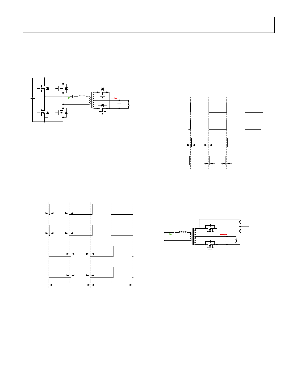
Data Sheet ADP1046
Q
A
Q
C
Q
D
Q
B
C
R
L
R
I
R
I
O
SR2
SR1
C
O
R
L
10045-037
PWM1 (OUTA)
PWM2 (OUTB)
PWM3 (OUTC)
PWM4 (OUTD)
t
A
t
B
t
C
Δt
1
Δt
2
Δt
3
Δt
4
Δt
5
Δt
6
Δt
7
Δt
8
t
PERIOD
t
PERIOD
10045-038
V
DS
(SR2)
ACSNS
SYNC RECT 1 (SR1)
SYNC RECT 2 (SR2)
t
D
t
E
t
F
Δt
9
Δt
10
Δt
11
Δt
12
10045-040
C
R
L
R
I
R
I
O
SR2
SR1
C
O
R
L
R
1
R
2
ACSNS
10045-039
RESONANT MODE OPERATION
The ADP1046 supports control of a resonant converter.
Resonant converters are an alternative to traditional fixed
frequency converters. They offer high switching frequency,
small size, and high efficiency. Figure 59 illustrates a widely
used series resonant converter.
SYNCHRONOUS RECTIFICATION IN RESONANT MODE
Control of the synchronous rectifiers in a resonant controller is
a complicated issue. The ADP1046 ACSNS comparator can be
used to control the SR signals. In resonant mode operation, the
SR1 output is driven by the rising edge of the ACSNS comparator,
and the SR2 output is driven by the falling edge of the comparator,
as shown in Figure 61.
Figure 59. Series Resonant Converter
RESONANT MODE ENABLE
To enable the ADP1046 to control a resonant switching converter, Register 0x40 must be set to a value of 0x3F. In resonant
mode, the PWM outputs have a fixed duty cycle with variable
frequency.
PWM TIMING IN RESONANT MODE
With variable frequency control, OUTA and OUTB can only be
high during the first half of the switching cycle (t
OUTC and OUTD can only be high during the second half of
the switching cycle (t
to tC), as shown in Figure 60. The
B
frequency resolution of the control law is in steps of 10 ns.
Figure 60. OUTA, OUTB, OUTC, and OUTD PWM Timing Diagram
in Resonant Mode
A
to tB), whereas
Rev. A | Page 87 of 96
Figure 61. SR1 and SR2 PWM Timing Diagram in Resonant Mode
Following is an example of how the ADP1046 can be used in a
series resonant topology and also achieve control of the synchronous rectifiers. The V
voltage of SR2 (see Figure 61) can be
DS
used to control the SR signals. The ACSNS pin is connected to
the divided-down SR2 V
voltage. This provides the timing
DS
information for both synchronous rectifiers (see Figure 62).
Figure 62. Resonant Synchronous Rectifier Control Circuit
After the timing information is obtained, SR1 is driven by the
rising edge of the ACSNS comparator, and SR2 is driven by the
falling edge of the comparator, as shown in Figure 61. In this
way, it is possible to achieve synchronous rectification. Turn-on
and turn-off delays can be programmed for the SR1 and SR2
signals individually.
This example is not the only way to control the SR signals. If the
user has another method to control the SR signals, this method
can be used to connect to the ACSNS input instead of the V
DS
voltage of SR2.
When the ADP1046 is used to control a resonant converter, it is
recommended that SR soft start be disabled during soft start of
the device (set Register 0x0F[7] = 1).

ADP1046 Data Sheet
ADJUSTING THE TIMING OF THE PWM OUTPUTS
To accurately adjust the timing of the PWM outputs, the
following registers can be used to set the dead time and delays
of the PWM outputs: Register 0x41, Register 0x43, Register 0x45,
Register 0x47, Register 0x49, Register 0x4B, Register 0x4D,
Register 0x4F, Register 0x51, Register 0x53, Register 0x55, and
Register 0x57. The resolution for adjusting the dead time is 5 ns.
Refer to the Resonant Mode Register Descriptions section for
more information. The software GUI for the ADP1046 can be
used to set the frequency limit registers, as well as all other
settings related to the resonant mode of operation.
FREQUENCY LIMIT SETTING
The minimum frequency is set by Register 0x42 and the first
four bits of Register 0x44.
For example, Register 0x42 is set to 0xA0 (160 decimal) and
Bits[7:4] of Register 0x44 are set to 0xF (15 decimal).
The maximum switching cycle is
(160 × 16 + 15) × 5 ns = 12.875 μs
The lowest switching frequency limit is
1/12.875 μs = 77.7 kHz
The maximum frequency is set by Register 0x46 and by
Bits[7:4] of Register 0x48.
For example, Register 0x46 is set to 0x10 (16 decimal) and
Bits[7:4] of Register 0x48 are set to 0x9 (9 decimal).
The minimum switching cycle is
(16 × 16 + 9) × 5 ns = 1.325 μs
The highest switching frequency limit is
1/1.325 μs = 755 kHz
FEEDBACK CONTROL IN RESONANT MODE
In contrast to a traditional fixed frequency PWM converter, the
output voltage of a resonant converter is regulated by changing
the switching frequency. When the ADP1046 is operated in
resonant mode, the switching frequency decreases when the
sensed voltage is lower than the reference voltage. This makes
the ADP1046 capable of controlling a resonant converter in
zero-voltage switching (ZVS) mode.
Although the switching frequency is variable, the high
frequency feedback voltage sampling frequency (VS3± pins)
is fixed at 400 kHz. The parameters of the feedback filter are
based on this frequency. The method for calculating the filter
parameters (gains, zeros, and poles) is the same as that for the
fixed frequency PWM mode (see the Digital Filter section).
SOFT START IN RESONANT MODE
During soft start, the reference voltage of the ADP1046 ramps
up. With the feedback loop closed, the switching frequency is
reduced from the highest limit to a regulation value. The soft
start timing settings and the filter settings are the same as those
for the fixed frequency PWM mode (see the Soft Start section).
LIGHT LOAD OPERATION (BURST MODE)
To control the converter at very light load, the ADP1046 can
operate in burst mode. Burst mode can be enabled or disabled
using Bits[7:6] of Register 0x4A. When the desired switching
frequency is higher than the burst mode threshold, the part
enters burst mode. The threshold is determined by the maximum frequency and the burst mode offset setting.
The threshold value used to enter burst mode is determined as
follows:
Threshold value for burst mode =
((Register 0x46 × 16) + Register 0x48[7:4]) +
(Register 0x4A[5:0] × 2)
The threshold value used to exit burst mode is determined by
the entrance value plus 0x10.
For example, Register 0x46 is set to 0x10 (16 decimal), Bits[7:4]
of Register 0x48 are set to 0, and Bits[5:0] of Register 0x4A are
set to 0x8 (8 decimal).
The minimum switching cycle is
(16 × 16 + 0) × 5 ns = 1.28 μs
The highest switching frequency limit is
1/1.28 μs = 781 kHz
The threshold to enter burst mode is
[(16 × 16 + 0) + (8 × 2)] × 5 ns = 1.36 μs
When the desired switching frequency is higher than
1/1.36 μs = 735 kHz, the PWM outputs are shut down
and the part enters burst mode.
The threshold to exit burst mode is
[(16 × 16 + 0) + (8 × 2) + 16] × 5 ns = 1.44 μs
Therefore, when the desired switching frequency becomes lower
than 1/1.44 μs = 694 kHz, the PWM signals are reenabled, and
the part exits burst mode.
OUTAUX IN RESONANT MODE
In resonant mode, the OUTAUX pin cannot be used as a control
signal. However, OUTAUX can be used as a fixed frequency
PWM signal with a fixed duty cycle.
PROTECTIONS IN RESONANT MODE
All of the flags and protections that are available in resonant mode
behave in the same manner as in fixed frequency PWM mode.
Rev. A | Page 88 of 96

Data Sheet ADP1046
[7:6]
Reserved
R/W
Reserved.
A
frequency limit is 1/12.875 μs = 77.7 kHz.
B
1 0 0 0 0 0 0 0
640 ns leading
Bits
Bit Name
R/W
Description
RESONANT MODE REGISTER DESCRIPTIONS
Table 153. Register 0x40—PWM Switching Frequency Setting in Resonant Mode
Bits Bit Name R/W Description
[5:0] Switching frequency R/W This register sets the switching frequency of the PWM pins and enables resonant mode. To
enable resonant mode, set these bits to 0x3F (111111).
Table 154. Register 0x41—OUTA Rising Edge Dead Time in Resonant Mode
Bits Bit Name R/W Description
[7:0] Δt1 (rising edge dead
time of OUTA)
0 0 0 0 0 0 0 0 0
0 0 0 0 0 0 0 1 5
… … … … … … … … …
1 1 1 1 1 1 1 1 1275
Table 155. Register 0x42—Lowest Switching Frequency Limit Setting (Maximum Switching Cycle in Resonant Mode)
Bits Bit Name R/W Description
[7:0] Lowest frequency R/W This register contains the eight MSBs of the 12-bit value of the lowest switching frequency (maxi-
R/W This register sets Δt1, which is the delay of the rising edge of OUTA from the start of the
switching cycle, t
Bit 7 Bit 6 Bit 5 Bit 4 Bit 3 Bit 2 Bit 1 Bit 0
mum switching cycle) limit. This value is always used with the top four bits of Register 0x44,
which contain the four LSBs of the lowest switching frequency limit. Each LSB of the 12-bit
value corresponds to 5 ns of resolution for the switching cycle. For example, if Register 0x42
is set to 0xA0 (160 decimal) and Bits[7:4] of Register 0x44 are set to 0xF (15 decimal), the
maximum switching cycle is (160 × 16 + 15) × 5 ns = 12.875 μs, and the lowest switching
. Each LSB corresponds to 5 ns of resolution.
Δt1 (ns)
Table 156. Register 0x43—OUTA Falling Edge Dead Time in Resonant Mode
Bits Bit Name R/W Description
[7:0] Δt2 (falling edge dead
time of OUTA)
Bit 7 Bit 6 Bit 5 Bit 4 Bit 3 Bit 2 Bit 1 Bit 0 Δt2
0 0 0 0 0 0 0 0 0 ns
0 0 0 0 0 0 0 1 5 ns trailing
… … … … … … … … …
0 1 1 1 1 1 1 1 635 ns trailing
… … … … … … … … …
1 1 1 1 1 1 1 1 5 ns leading
R/W This register sets Δt2, which is the difference between the falling edge of OUTA and the mid-
point of the switching cycle, tB. Each LSB corresponds to 5 ns of resolution. When the register
value is from 0x00 to 0x7F, the falling edge of OUTA is trailing t
to 0xFF, the falling edge of OUTA is leading t
.
. When the value is from 0x80
B
Table 157. Register 0x44—Lowest Switching Frequency Limit Setting (Maximum Switching Cycle in Resonant Mode)
[7:4] Lowest frequency R/W This register contains the four LSBs of the 12-bit value of the lowest switching frequency (maxi-
mum switching cycle) limit. This value is always used with the eight bits of Register 0x42, which
contain the eight MSBs of the lowest switching frequency limit. Each LSB of the 12-bit value
corresponds to 5 ns of resolution for the switching cycle. For example, if Register 0x42 is set
to 0xA0 (160 decimal) and Bits[7:4] of Register 0x44 are set to 0xF (15 decimal), the maximum
switching cycle is (160 × 16 + 15) × 5 ns = 12.875 μs, and the lowest switching frequency limit
is 1/12.875 μs = 77.7 kHz.
[3:0] Reserved R/W Reserved.
Rev. A | Page 89 of 96

ADP1046 Data Sheet
Table 158. Register 0x45—OUTB Rising Edge Dead Time in Resonant Mode
Bits Bit Name R/W Description
[7:0]
(rising edge dead
Δt
3
time of OUTB)
0 0 0 0 0 0 0 0 0
0 0 0 0 0 0 0 1 5
… … … … … … … … …
1 1 1 1 1 1 1 1 1275
Table 159. Register 0x46—Highest Switching Frequency Limit Setting (Minimum Switching Cycle in Resonant Mode)
Bits Bit Name R/W Description
[7:0] Highest frequency R/W
Table 160. Register 0x47—OUTB Falling Edge Dead Time in Resonant Mode
Bits Bit Name R/W Description
[7:0]
(falling edge dead
Δt
4
time of OUTB)
Bit 7 Bit 6 Bit 5 Bit 4 Bit 3 Bit 2 Bit 1 Bit 0 Δt4
0 0 0 0 0 0 0 0 0 ns
0 0 0 0 0 0 0 1 5 ns trailing
… … … … … … … … …
0 1 1 1 1 1 1 1 635 ns trailing
1 0 0 0 0 0 0 0 640 ns leading
… … … … … … … … …
1 1 1 1 1 1 1 1 5 ns leading
R/W
R/W
This register sets Δt
switching cycle, t
Bit 7 Bit 6 Bit 5 Bit 4 Bit 3 Bit 2 Bit 1 Bit 0 Δt
, which is the delay time of the rising edge of OUTB from the start of the
3
. Each LSB corresponds to 5 ns of resolution.
A
(ns)
3
This register contains the eight MSBs of the 12-bit value of the highest switching frequency (minimum switching cycle) limit. This value is always used with the top four bits of Register 0x48,
which contain the four LSBs of the highest switching frequency limit. Each LSB of the 12-bit
value corresponds to 5 ns of resolution for the switching cycle. For example, if Register 0x46
is set to 0x10 (16 decimal) and Bits[7:4] of Register 0x48 are set to 0x9 (9 decimal), the minimum
switching cycle is (16 × 16 + 9) × 5 ns = 1.325 μs, and the highest switching frequency limit is
1/1.325 μs = 755 kHz. It is recommended that the maximum frequency be limited to 1 MHz.
This register sets Δt
point of the switching cycle, t
value is from 0x00 to 0x7F, the falling edge of OUTB is trailing t
to 0xFF, the falling edge of OUTB is leading t
, which is the difference between the falling edge of OUTB and the mid-
4
. Each LSB corresponds to 5 ns of resolution. When the register
B
.
B
. When the value is from 0x80
B
Table 161. Register 0x48—Highest Switching Frequency Limit Setting (Minimum Switching Cycle in Resonant Mode)
Bits Bit Name R/W Description
[7:4] Highest frequency R/W
This register contains the four LSBs of the 12-bit value of the highest switching frequency (minimum switching cycle) limit. This value is always used with the eight bits of Register 0x46, which
contain the eight MSBs of the highest switching frequency limit. Each LSB of the 12-bit value
corresponds to 5 ns of resolution for the switching cycle. For example, if Register 0x46 is set to
0x10 (16 decimal) and Bits[7:4] of Register 0x48 are set to 0x9 (9 decimal), the minimum
switching cycle is (16 × 16 + 9) × 5 ns = 1.325 μs, and the highest switching frequency limit is
1/1.325 μs = 755 kHz.
[3:0] Reserved R/W Reserved.
Rev. A | Page 90 of 96

Data Sheet ADP1046
B
1 1
Enabled for normal operation and during soft start
C
B
1 1 1 1 1 1 1 1
5 ns leading
Table 162. Register 0x49—OUTC Rising Edge Dead Time in Resonant Mode
Bits Bit Name R/W Description
[7:0] Δt5 (rising edge dead
time of OUTC)
0 0 0 0 0 0 0 0 0 ns
0 0 0 0 0 0 0 1 5 ns trailing
… … … … … … … … …
0 1 1 1 1 1 1 1 635 ns trailing
1 0 0 0 0 0 0 0 640 ns leading
… … … … … … … … …
1 1 1 1 1 1 1 1 5 ns leading
Table 163. Register 0x4A—Burst Mode Operation in Resonant Mode
Bits Bit Name R/W Description
[7:6] Burst mode enable R/W These bits are used to enable or disable burst mode operation.
0 0 Disabled
0 1 Enabled for normal operation, but disabled during soft start
1 0 Disabled
R/W This register sets Δt5, which is the difference between the rising edge of OUTC and the mid-
point of the switching cycle, t
. Each LSB corresponds to 5 ns of resolution. When the register
B
value is from 0x00 to 0x7F, the rising edge of OUTC is trailing tB. When the value is from 0x80
to 0xFF, the rising edge of OUTC is leading t
Bit 7 Bit 6 Bit 5 Bit 4 Bit 3 Bit 2 Bit 1 Bit 0
.
Δt5
Bit 7 Bit 6 Burst Mode
[5:0] Burst mode offset R/W These bits, along with the highest switching frequency limit, determine the threshold value for
enabling burst mode operation. For information about how to set this value, see the Light Load
Operation (Burst Mode) section. During burst mode, the PWM frequency is the maximum
frequency limit set in Register 0x46.
Table 164. Register 0x4B—OUTC Falling Edge Dead Time in Resonant Mode
Bits Bit Name R/W Description
[7:0] Δt6 (falling edge dead
time of OUTC)
R/W This register sets Δt6, which is the leading time of the falling edge of OUTC from the end of the
switching cycle, t
. Each LSB corresponds to 5 ns of resolution.
Bit 7 Bit 6 Bit 5 Bit 4 Bit 3 Bit 2 Bit 1 Bit 0 Δt6 (ns)
0 0 0 0 0 0 0 0 0
0 0 0 0 0 0 0 1 5
… … … … … … … … …
1 1 1 1 1 1 1 1 1275
Table 165. Register 0x4D—OUTD Rising Edge Dead Time in Resonant Mode
Bits Bit Name R/W Description
[7:0] Δt7 (rising edge dead
time of OUTD)
R/W This register sets Δt7, which is the difference between the rising edge of OUTD and the mid-
point of the switching cycle, tB. Each LSB corresponds to 5 ns of resolution. When the register
value is from 0x00 to 0x7F, the rising edge of OUTD is trailing t
to 0xFF, the rising edge of OUTD is leading t
.
. When the value is from 0x80
B
Bit 7 Bit 6 Bit 5 Bit 4 Bit 3 Bit 2 Bit 1 Bit 0 Δt7
0 0 0 0 0 0 0 0 0 ns
0 0 0 0 0 0 0 1 5 ns trailing
… … … … … … … … …
0 1 1 1 1 1 1 1 635 ns trailing
1 0 0 0 0 0 0 0 640 ns leading
… … … … … … … … …
Rev. A | Page 91 of 96

ADP1046 Data Sheet
C
0 0 0 0 0 0 0 0
0
D
… … … … … … … …
…
E
E
F
Table 166. Register 0x4F—OUTD Falling Edge Dead Time in Resonant Mode
Bits Bit Name R/W Description
[7:0] Δt8 (falling edge dead
time of OUTD)
Bit 7 Bit 6 Bit 5 Bit 4 Bit 3 Bit 2 Bit 1 Bit 0 Δt8 (ns)
0 0 0 0 0 0 0 1 5
… … … … … … … … …
1 1 1 1 1 1 1 1 1275
Table 167. Register 0x51—SR1 Rising Edge Dead Time in Resonant Mode
Bits Bit Name R/W Description
[7:0] Δt9 (rising edge dead
time of SR1)
Bit 7 Bit 6 Bit 5 Bit 4 Bit 3 Bit 2 Bit 1 Bit 0 Δt9 (ns)
0 0 0 0 0 0 0 0 0
0 0 0 0 0 0 0 1 5
1 1 1 1 1 1 1 1 1275
Table 168. Register 0x53—SR1 Falling Edge Dead Time in Resonant Mode
Bits Bit Name R/W Description
[7:0] Δt10 (falling edge
dead time of SR1)
0 0 0 0 0 0 0 0 0
0 0 0 0 0 0 0 1 5
… … … … … … … … …
1 1 1 1 1 1 1 1 1275
R/W This register sets Δt8, which is the leading time of the falling edge of OUTD from the end of the
switching cycle, t
. Each LSB corresponds to 5 ns of resolution.
R/W This register sets Δt9, which is the delay time of the rising edge of SR1 from the ACSNS rising
. Each LSB corresponds to 5 ns of resolution.
edge, t
R/W This register sets Δt10, which is the leading time of the falling edge of SR1 from the ACSNS
falling edge, t
Bit 7 Bit 6 Bit 5 Bit 4 Bit 3 Bit 2 Bit 1 Bit 0
. Each LSB corresponds to 5 ns of resolution.
Δt10 (ns)
Table 169. Register 0x55—SR2 Rising Edge Dead Time in Resonant Mode
Bits Bit Name R/W Description
[7:0] Δt11 (rising edge dead
time of SR2)
R/W This register sets Δt11, which is the delay time of the rising edge of SR2 from the ACSNS falling
edge, t
. Each LSB corresponds to 5 ns of resolution.
Bit 7 Bit 6 Bit 5 Bit 4 Bit 3 Bit 2 Bit 1 Bit 0 Δt11 (ns)
0 0 0 0 0 0 0 0 0
0 0 0 0 0 0 0 1 5
… … … … … … … … …
1 1 1 1 1 1 1 1 1275
Table 170. Register 0x57—SR2 Falling Edge Dead Time in Resonant Mode
Bits Bit Name R/W Description
[7:0] Δt12 (falling edge
dead time of SR2)
R/W This register sets Δt12, which is the leading time of the falling edge of SR2 from the ACSNS rising
edge, t
. Each LSB corresponds to 5 ns of resolution.
Bit 7 Bit 6 Bit 5 Bit 4 Bit 3 Bit 2 Bit 1 Bit 0 Δt12 (ns)
0 0 0 0 0 0 0 0 0
0 0 0 0 0 0 0 1 5
… … … … … … … … …
1 1 1 1 1 1 1 1 1275
Rev. A | Page 92 of 96

Data Sheet ADP1046
COMPLI ANT TO JEDEC STANDARDS MO-220-WHHD.
112408-A
1
0.50
BSC
BOTTOM VIEWTOP VIEW
PIN 1
INDICATOR
32
9
16
17
24
25
8
EXPOSED
PAD
PIN 1
INDICATOR
3.25
3.10 SQ
2.95
SEATING
PLANE
0.05 MAX
0.02 NOM
0.20 REF
COPLANARITY
0.08
0.30
0.25
0.18
5.10
5.00 SQ
4.90
0.80
0.75
0.70
FOR PROP E R CONNECTION OF
THE EXPOSED PAD, REFER TO
THE PIN CO NFIGURATI ON AND
FUNCTIO N DE S CRIPTIONS
SECTION OF THIS DATA SHEET.
0.50
0.40
0.30
0.25 MIN
Model1
Temperature Range
Package Description
Package Option
ADP1046ACPZ-RL
−40°C to +125°C
32-Lead Lead Frame Chip Scale Package [LFCSP_WQ]
CP-32-7
OUTLINE DIMENSIONS
Figure 63. 32-Lead Lead Frame Chip Scale Package [LFCSP_WQ]
5 mm × 5 mm Body, Very Very Thin Quad
(CP-32-7)
Dimensions shown in millimeters
ORDERING GUIDE
ADP1046ACPZ-R7 −40°C to +125°C 32-Lead Lead Frame Chip Scale Package [LFCSP_WQ] CP-32-7
ADP1046-100-EVALZ ADP1046 100 W Evaluation Board
ADP1046DC1-EVALZ ADP1046 Daughter Card
ADP-I2C-USB-Z USB to I2C Adapter
1
Z = RoHS Compliant Part.
Rev. A | Page 93 of 96

ADP1046 Data Sheet
NOTES
Rev. A | Page 94 of 96

Data Sheet ADP1046
NOTES
Rev. A | Page 95 of 96

ADP1046 Data Sheet
©2012 Analog Devices, Inc. All rights reserved. Trademarks and
NOTES
I2C refers to a communications protocol originally developed by Philips Semiconductors (now NXP Semiconductors).
registered trademarks are the property of their respective owners.
D10045-0-6/12( A)
Rev. A | Page 96 of 96
 Loading...