

Digital Controller for Isolated
T
FEATURES
Integrates all typical controller functions
Digital control loop
Remote and local voltage sense
Primary and secondary side current sense
PWM control
Synchronous rectifier control
Current sharing
Integrated programmable loop filter
2
I
C interface
Extensive fault detection and protection
Extensive programming
Fast calibration
EEPROM
Standalone or microcontroller control
APPLICATIONS
AC-to-DC power supplies
Isolated dc-to-dc power supplies
Redundant power supplies
Parallel power supplies
Server, storage, network, and communications infrastructure
Power Supply Applications
ADP1043A
GENERAL DESCRIPTION
The ADP1043A is a secondary side power supply controller IC
designed to provide all the functions that are typically needed in
an ac-to-dc or isolated dc-to-dc control application.
The ADP1043A is optimized for minimal component count,
maximum flexibility, and minimum design time. Features
include remote voltage sense, local voltage sense, primary and
secondary side current sense, pulse-width modulation (PWM)
generation, and hot-swap sense and control. The control loop is
digital with an integrated programmable digital filter. Protection
features include current limiting, ac sense, undervoltage lockout
(UVLO), and overvoltage protection (OVP).
The built-in EEPROM provides extensive programming of the
integrated loop filter, PWM signal timing, inrush current, and
soft start timing and sequencing. Reliability is improved through
a built-in checksum and redundancy of critical circuits.
A comprehensive GUI is provided for easy design of loop filter
characteristics and programming of the safety features. The
industry-standard I
toring and system test functions.
The ADP1043A is available in a 32-lead LFCSP and operates
from a single 3.3 V supply.
2
C bus provides access to the many moni-
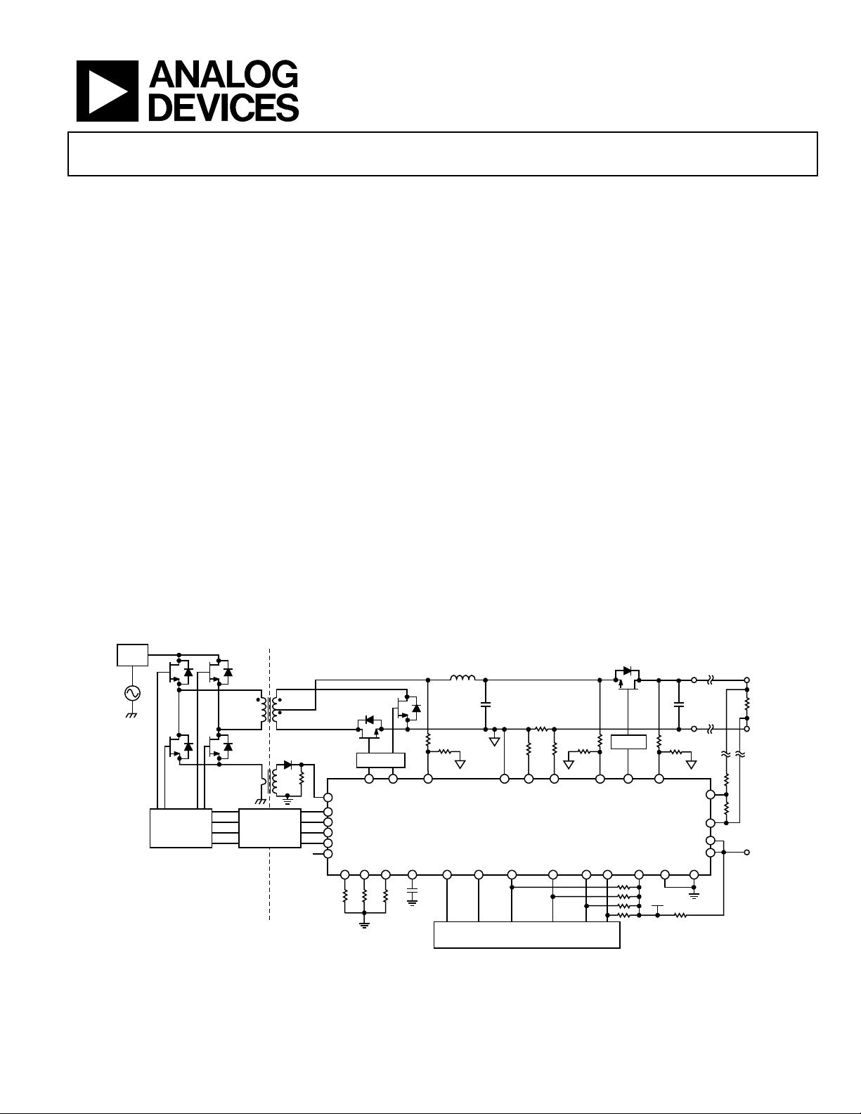
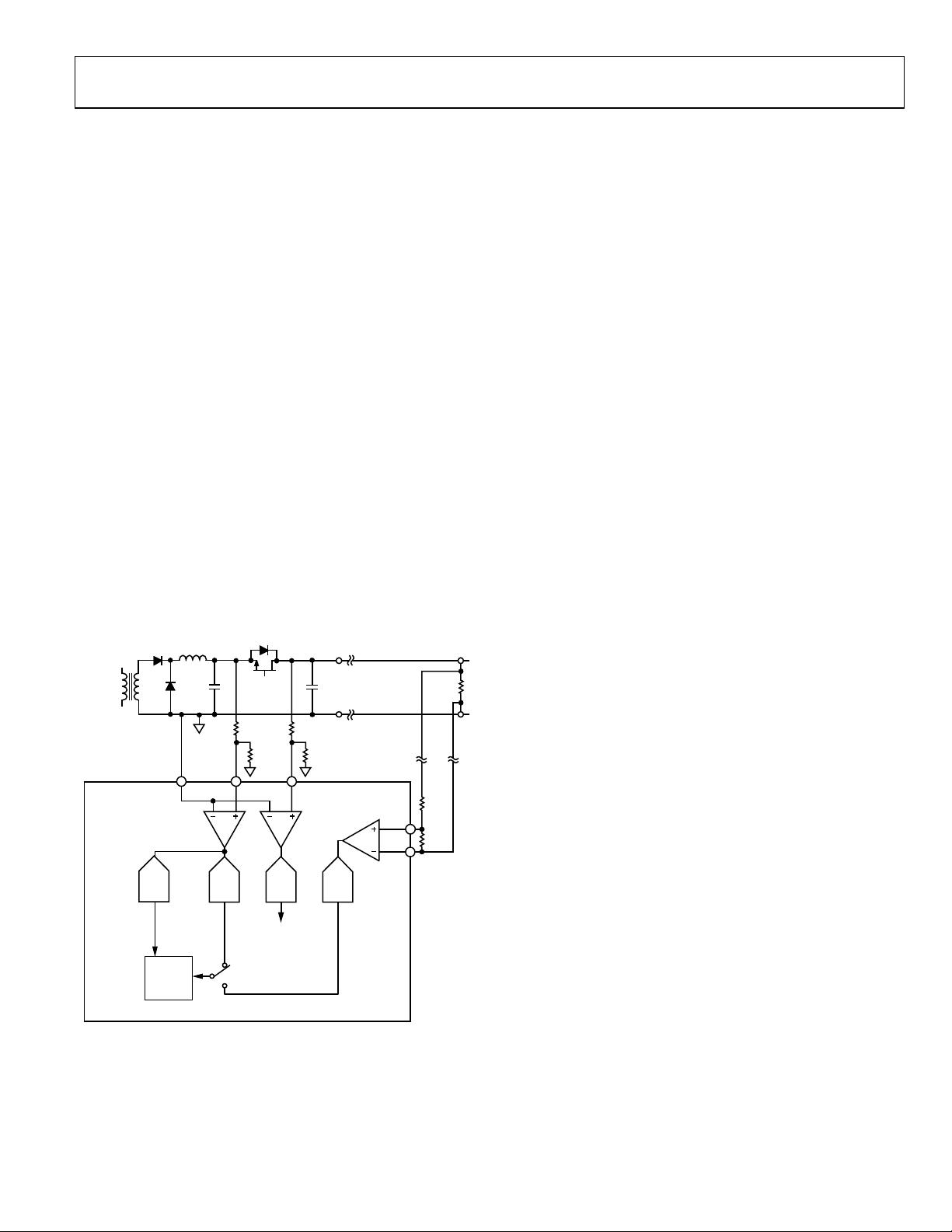
TYPICAL APPLICATION CIRCUIT
PFC
AC
INPU
DRIVER
SR1 SR2 ACSNS PGND
CS1
OUTA
DRIVER
Rev. 0
Information furnished by Analog Devices is believed to be accurate and reliable. However, no
responsibility is assumed by Analog Devices for its use, nor for any infringements of patents or other
rights of third parties that may result from its use. Specifications subject to change without notice. No
license is granted by implication or otherwise under any patent or patent rights of Analog Devices.
Trademarks and registered trademarks are the property of their respective owners.
ADuM1410
OUTB
OUTC
OUTD
OUTAUX
RES RTDADD VCORE FLAGIN PSON PGOOD2 PGOOD1 SDA SCL VDD DGND AGND
DRIVER
GATE
CS2– CS2+
MICROCONTROLLER
Figure 1.
One Technology Way, P.O. Box 9106, Norwood, MA 02062-9106, U.S.A.
Tel: 781.329.4700 www.analog.com
Fax: 781.461.3113 ©2009 Analog Devices, Inc. All rights reserved.
VS1
VS2
V
DD
VS3+
VS3–
SHAREo
SHAREi
LOAD
08501-001

ADP1043A
TABLE OF CONTENTS
Features .............................................................................................. 1
Applications ....................................................................................... 1
General Description ......................................................................... 1
Typical Application Circuit ............................................................. 1
Revision History ............................................................................... 3
Functional Block Diagram .............................................................. 4
Specifications ..................................................................................... 5
Absolute Maximum Ratings ............................................................ 8
Thermal Resistance ...................................................................... 8
Soldering ........................................................................................ 8
ESD Caution .................................................................................. 8
Pin Configuration and Function Descriptions ............................. 9
Typical Performance Characteristics ........................................... 11
Theory of Operation ...................................................................... 12
Current Sense .............................................................................. 12
Voltage Sense and Control Loop .............................................. 13
ADCs ............................................................................................ 13
Digital Filter ................................................................................ 14
PWM and Sync Rect Outputs (OUTA, OUTB, OUTC,
OUTD, OUTAUX, SR1, SR2) ................................................... 14
Synchronous Rectification ........................................................ 15
Adaptive Dead Time Control.................................................... 15
Light Load Mode ........................................................................ 15
Modulation Limit ....................................................................... 15
OrFET Control (GATE) ............................................................ 15
VDD ............................................................................................. 18
VDD/VCORE OVLO ................................................................ 18
Power Good ................................................................................. 18
Soft Start ...................................................................................... 19
Current Sharing (Share) ............................................................ 20
Power Supply System and Fault Monitoring ............................... 22
Flags .............................................................................................. 22
Monitoring Functions ................................................................ 22
Voltage Readings ........................................................................ 22
Current Readings ........................................................................ 22
Power Readings ........................................................................... 23
Power Monitoring Accuracy ..................................................... 23
First Flag Fault ID and Value Registers ................................... 23
External Flag Input (FLAGIN Pin) .......................................... 23
Temperature Readings (RTD Pin) ............................................ 23
Overtemperature Protection (OTP) ........................................ 23
Overcurrent Protection (OCP) ................................................ 24
Constant Current Mode ............................................................ 25
Overvoltage Protection (OVP) ................................................. 25
Undervoltage Protection (UVP) .............................................. 25
AC Sense (ACSNS)..................................................................... 26
Volt-Second Balance .................................................................. 26
Load Line ..................................................................................... 26
Power Supply Calibration and Trim ............................................ 27
CS1 Trim ...................................................................................... 27
CS2 Trim ...................................................................................... 27
Voltage Calibration and Trim ................................................... 27
Output Voltage Setting (VS3+, VS3− Trim) ........................... 28
VS1 Trim ...................................................................................... 28
VS2 Trim ...................................................................................... 28
RTD/OTP Trim .......................................................................... 28
Layout Guidelines....................................................................... 28
Communication .............................................................................. 29
I2C Interface ................................................................................ 29
EEPROM ..................................................................................... 31
Software GUI .............................................................................. 32
Register Listing ............................................................................... 33
Detailed Register Descriptions ..................................................... 35
Fault Registers ............................................................................. 35
Value Registers ............................................................................ 38
Current Sense and Current Limit Registers ............................ 41
Voltage Sense Registers .............................................................. 46
ID Registers ................................................................................. 49
PWM and Synchronous Rectifier Timing Registers ............. 50
Digital Filter Programming Registers ...................................... 58
Adaptive Dead Time Registers ................................................. 60
EEPROM Registers .................................................................... 64
Resonant Mode Operation ............................................................ 65
Resonant Mode Enable .............................................................. 65
PWM Timing in Resonant Mode ............................................. 65
Synchronous Rectification in Resonant Mode ....................... 65
Adjusting the Timing of the PWM Outputs ........................... 66
Frequency Limit Setting ............................................................ 66
Feedback Control in Resonant Mode ...................................... 66
Soft Start in Resonant Mode ..................................................... 66
Rev. 0 | Page 2 of 72

ADP1043A
Light Load Operation (Burst Mode) ........................................ 66
OUTAUX in Resonant Mode .................................................... 66
Protections in Resonant Mode .................................................. 66
REVISION HISTORY
10/09—Revision 0: Initial Version
Resonant Mode Register Descriptions ..................................... 67
Outline Dimensions ........................................................................ 71
Ordering Guide ........................................................................... 71
Rev. 0 | Page 3 of 72
ADP1043A
The ADP1043A is a secondary side controller for switch mode
power supplies (SMPS). It is designed for use in isolated redundant applications. The ADP1043A integrates the typical functions
that are needed to control a power supply. These include
• Output voltage sense and feedback
• Digital loop filter compensation
• PWM generation
• Current sharing
• Current, voltage, and temperature sense
• OrFET control
• Housekeeping and I
2
C interface
• Calibration and trimming
The main function of controlling the output voltage is performed
using the feedback ADCs, the digital loop filter, and the PWM
block. The feedback ADCs use a multipath approach (patent
pending). The ADP1043A combines a high speed, low resolution
(fast and coarse) ADC and a low speed, high resolution (slow and
accurate) ADC. Loop compensation is implemented using the
digital filter. This PID (proportional, integral, derivative) filter is
implemented in the digital domain to allow easy programming
of filter characteristics, which is of great value in customizing
and debugging designs.
The PWM block generates up to seven programmable PWM
outputs for control of FET drivers and synchronous rectification
FET drivers. This programmability allows many traditional and
unique switching topologies to be realized.
A current share bus interface provides for parallel power supplies.
The part also has hot-swap OrFET sense and control for N + 1
redundant power supplies.
Conventional power supply housekeeping features, such as remote
and local voltage sense and primary and secondary side current
sense, are included. An extensive set of protections is offered,
including overvoltage protection (OVP), overcurrent protection
(OCP), overtemperature protection (OTP), undervoltage protection (UVP), ground continuity monitoring, and ac sense.
All these features are programmable through the I
2
C bus interface. This bus interface is also used to calibrate the power supply.
Other information, such as input current, output current, and
fault flags, is also available through the I
2
C bus interface.
The internal EEPROM can store all programmed values and
allows standalone control without a microcontroller. A free,
downloadable GUI is available that provides all the necessary
software to program the ADP1043A. For more information
about the GUI, contact Analog Devices, Inc., for the latest
software and a user guide.
The ADP1043A operates from a single 3.3 V supply and is
specified from −40°C to +85°C.
CS1
SR1
SR2
OUTA
OUTB
OUTC
OUTD
OUTAUX
VDD
VCORE
RES
AGND
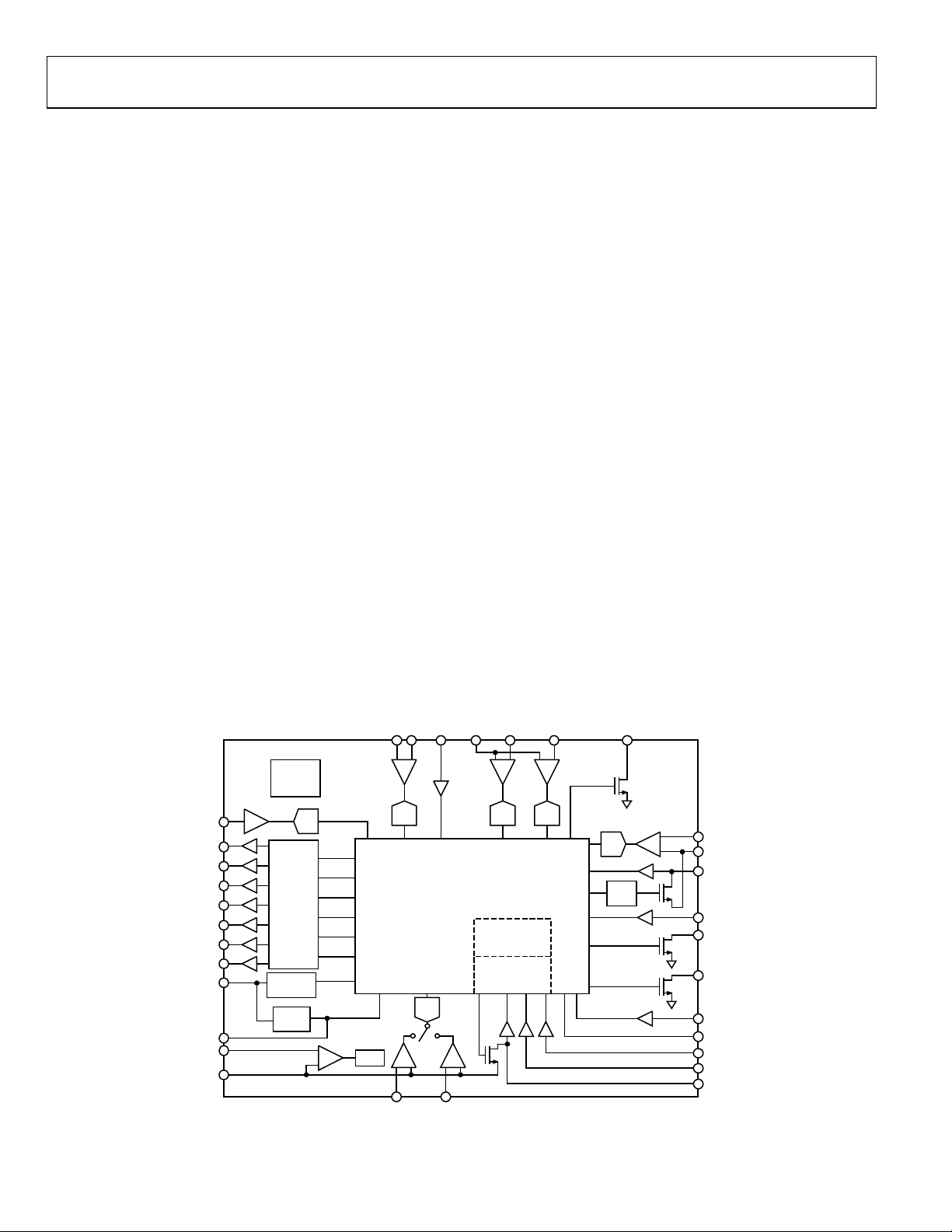
VREF
ADC
PWM
ENGINE
UVLO
LDO
FUNCTIONAL BLOCK DIAGRAM
PGND
ADC
8kB
EEPROM
2
I
C
INTERFACE
VS1
VS2
ADC
OSC
CS2–
ADC
CS2+
ADC
ACSNS
DIGITAL
CORE
RTDADD
Figure 2.
ADC
PWM
GATE
VS3+
VS3–
SHAREo
SHAREi
PGOOD1
PGOOD2
FLAGIN
DGND
PSON
SCL
SDA
08501-002
Rev. 0 | Page 4 of 72

ADP1043A
SPECIFICATIONS
VDD = 3.3 V, TA = −40°C to +85°C, unless otherwise noted. FSR = full-scale range.
Table 1.
Parameter Symbol Test Conditions/Comments Min Typ Max Unit
SUPPLY
VDD V
IDD I
Power supply off (PSON is low) 15 mA
During EEPROM programming (40 ms) IDD + 8 mA
POWER-ON RESET
Power-On Reset VDD rising 3.05 V
UVLO VDD falling 2.75 2.85 2.95 V
UVLO Hysteresis 35 mV
OVLO 3.7 3.9 4.1 V
VCORE PIN
Output Voltage TA = 25°C 2.3 2.5 2.7 V
OSCILLATOR AND PLL
PLL Frequency RES = 49.9 kΩ 190 200 210 MHz
OUTA, OUTB, OUTC, OUTD,
OUTAUX, SR1, SR2 PINS
Output Low Voltage VOL Source current = 10 mA 0.4 V
Output High Voltage VOH Source current = 10 mA VDD − 0.4 V
Rise Time C
Fall Time C
AC SENSE PWM and resonant mode
Input Voltage Threshold 0.3 0.45 0.65 V
Propagation Delay
VS1, VS2, VS3 LOW SPEED ADC
Input Voltage Range VIN
Sampling Frequency f
Voltage Sense Measurement
Accuracy
−155 +155 mV
From 10% to 90% of input voltage range −2.5 +2.5 % FSR
−38.75 +38.75 mV
From 900 mV to 1.1 V −1.5 +1.5 % FSR
−23.25 +23.25 mV
Voltage Sense Measurement
Resolution
Voltage Differential from VS3−
to PGND
VS1 OVP Comparator Speed Register 0x2C[2] = 0 300 s
VS1 OVP Threshold Accuracy Relative to nominal voltage (1 V) on VS1 2.5 %
VS2 and VS3 OVP Comparator
Speed
VS2 and VS3 OVP Threshold
Accuracy
VS1 HIGH SPEED ADC
Sampling Frequency f
Resolution 6 Bits
Dynamic Range ±18 mV
3.1 3.3 3.6 V
DD
Normal operation (PSON is high) 20 mA
DD
= 50 pF 3.5 ns
LOAD
= 50 pF 1.5 ns
LOAD
From ACSNS threshold to SR start;
160 ns
resonant mode only
Differential voltage from VS1, VS2 to PGND,
0 1 1.55 V
and from VS3+ to VS3−
100 Hz
SAMP
From 0% to 100% of input voltage range −10 +10 % FSR
12 Bits
−200 +200 mV
Register 0x2C[2] = 0 300 s
Relative to nominal voltage (1 V) on VS2
2.5 %
and VS3
400 kHz
SAMP
Rev. 0 | Page 5 of 72

ADP1043A
Parameter Symbol Test Conditions/Comments Min Typ Max Unit
CURRENT SENSE 1 (CS1 PIN)
Input Voltage Range VIN 0 1 1.38 V
Sampling Frequency f
Current Sense Measurement
Accuracy
−41.4 +41.4 mV
From 0% to 100% of input voltage range −10 +10 % FSR
−138 +138 mV
Current Sense Measurement
Resolution
CS1 Fast OCP Threshold 1.1 1.2 1.3 V
CS1 Fast OCP Speed 80 100 ns
CS1 Accurate OCP DC Accuracy From 10% to 90% of input voltage range −3.0 +3.0 % FSR
−41.4 +41.4 mV
CS1 Accurate OCP Speed 10 ms
Leakage Current 4.0 A
CURRENT SENSE 2 (CS2+, CS2−
PINS)
Input Voltage Range VIN Differential voltage from CS2+ to CS2− −100 +225 mV
ADC Input Voltage Range LSB = 61.04 V 0 225 mV
Sampling Frequency f
Current Sense Measurement
Accuracy
From 200 mV to 225 mV −15 +15 mV
−7.5 +7.5 % FSR
Current Sense Measurement
Resolution
CS2 Accurate OCP Accuracy From 0 mV to 200 mV −4 +4 mV
From 200 mV to 225 mV −15 +15 mV
−7.5 +7.5 % FSR
CS2 Accurate OCP Speed 10 ms
Current Sink (High Side) 100 A
Current Source (Low Side) 100 A
Common-Mode Voltage at the
CS2+ and CS2− Pins
GATE PIN (OPEN DRAIN)
Output Low Voltage VOL 0.4 V
OrFET PROTECTION (CS2+, CS2−) Low-side current sensing only
Accurate OrFET Threshold
Accuracy
Accurate OrFET Speed 10 ms
Fast OrFET Accuracy −25 mV setting −40 −25 −10 mV
−50 mV setting −70 −50 −30 mV
−75 mV setting −100 −75 −50 mV
−100 mV setting −125 −100 −75 mV
Fast OrFET Speed Debounce = 40 ns 110 150 ns
RTD PIN
Input Voltage Range VIN 0 1 1.55 V
Current Source RTD resistor = 100 kΩ 9.5 10.8 12 A
RTD ADC Measurement
Accuracy
From 32 mV to 320 mV −15.5 +15.5 mV
From 0% to 100% of input voltage range −10 +10 % FSR
From 0 V to 1.55 V −155 +155 mV
100 Hz
SAMP
From 10% to 90% of input voltage range −3.0 +3.0 % FSR
12 Bits
100 Hz
SAMP
From 0 mV to 200 mV −4 +4 mV
12 Bits
To achieve CS2 measurement accuracy 0.8 1 1.3 V
−1.2 0 +1 mV
From 2% to 20% of input voltage range −1 +1 % FSR
Rev. 0 | Page 6 of 72

ADP1043A
Parameter Symbol Test Conditions/Comments Min Typ Max Unit
OTP Threshold Accuracy When RTD = 10 kΩ −0.5 +0.5 % FSR
−7.75 +7.75 mV
When RTD = 100 kΩ −5 +5 % FSR
−77.5 +77.5 mV
OTP Speed 10 ms
OTP Threshold Hysteresis When RTD = 10 kΩ 16 mV
PGOOD1, PGOOD2, SHAREo PINS
(OPEN DRAIN)
Output Low Voltage VOL 0.4 V
PSON, FLAGIN, SHAREi PINS
(DIGITAL INPUTS)
Input Low Voltage VIL 0.4 V
Input High Voltage VIH V
SDA/SCL PINS VDD = 3.3 V
Input Low Voltage VIL 0.4 V
Input High Voltage VIH V
Output Low Voltage VOL 0.4 V
Leakage Current −5 +5 µA
SERIAL BUS TIMING
Clock Frequency 100 400 kHz
Glitch Immunity tSW 50 ns
Bus-Free Time t
Start Setup Time t
Start Hold Time t
SCL Low Time t
SCL High Time t
SCL, SDA Rise Time tR 1000 ns
SCL, SDA Fall Time tF 300 ns
Data Setup Time t
Data Hold Time t
EEPROM RELIABILITY
1
Endurance
Data Retention
1
Endurance is qualified as per JEDEC Standard 22, Method A117, and is measured at −40°C, +25°C, +85°C, and +125°C.
2
Retention lifetime equivalent at junction temperature (TJ) = 85°C as per JEDEC Standard 22, Method A117. Retention lifetime derates with junction temperature.
2
− 0.8 V
DD
− 0.8 V
DD
4.7 µs
BUF
4.7 µs
SU;STA
4 µs
HD;STA
4.7 µs
LOW
4 µs
HIGH
250 ns
SU;DAT
300 ns
HD;DAT
10,000 Cycles
T
= 85°C 20 Years
J
Rev. 0 | Page 7 of 72

ADP1043A
ABSOLUTE MAXIMUM RATINGS
Table 2.
Parameter Rating
Supply Voltage (Continuous) VDD 4.2 V
Digital Pins −0.3 V to VDD + 0.3 V
VS3− to PGND, AGND, DGND −0.3 V to +0.3 V
RTD, VS1 to AGND 2.5 V
VS2, VS3+, ADD to AGND −0.3 V to VDD + 0.3 V
Operating Temperature Range −40°C to +85°C
Storage Temperature Range −65°C to +150°C
Junction Temperature 150°C
Peak Solder Reflow Temperature
SnPb Assemblies (10 sec to 30 sec) 240°C
RoHS-Compliant Assemblies
(20 sec to 40 sec)
ESD Charged Device Model 1.5 kV
ESD Human Body Model 3.5 kV
Stresses above those listed under Absolute Maximum Ratings
may cause permanent damage to the device. This is a stress
rating only; functional operation of the device at these or any
other conditions above those indicated in the operational
section of this specification is not implied. Exposure to absolute
maximum rating conditions for extended periods may affect
device reliability.
260°C
THERMAL RESISTANCE
θJA is specified for the worst-case conditions, that is, a device
soldered in a circuit board for surface-mount packages.
Table 3. Thermal Resistance
Package Type θJA θ
32-Lead LFCSP 44.4 6.4 °C/W
Unit
JC
SOLDERING
It is important to follow the correct guidelines when laying out
the PCB footprint for the ADP1043A and when soldering the
part onto the PCB. The AN-772 Application Note discusses this
topic in detail (see www.analog.com).
ESD CAUTION
Rev. 0 | Page 8 of 72

ADP1043A
PIN CONFIGURATION AND FUNCTION DESCRIPTIONS
RTD
VS3+
32
VDD
RES
ADD
VCORE
VS3–
31
30
DGND
29
28
27
26
25
14
OUTD
15
16
GATE
OUTAUX
24 SHAREi
23 SHAREo
22 PGOOD1
21 PGOOD2
20 FLAGIN
19 PSON
18 SDA
17 SCL
08501-003
1VS2
PIN 1
2AGND
INDICATOR
3VS1
4CS2–
TOP VIEW
5CS2+
(Not to S cal e)
6ACSNS
7CS1
8PGND
9
11
12
13
10
SR1
SR2
UTB
OUTA
O
OUTC
NOTES
1. THE ADP1043A HAS AN EXPOSED THERMAL PAD ON THE UNDERSIDE
OF THE PACKAG E . FOR INCREASED RELIABIL ITY OF THE SOLDER
JOINTS AND MAX IMUM THERMAL CAPABILITY , IT IS RECOMMENDED
THAT THE PAD BE S OLDERED TO THE PCB GROUND PL ANE .
Figure 3. Pin Configuration
Table 4. Pin Function Descriptions
Pin No. Mnemonic Description
1 VS2
Power Supply Output Sense Input. This signal is referred to PGND. Input to a low frequency Σ-∆ ADC. Nominal
voltage at this pin should be 1 V. The resistor divider on this input must have a tolerance specification of 0.5%
or better to allow for trimming.
2 AGND Analog Ground. This pin is the ground for the analog circuitry of the ADP1043A. Star connect to DGND.
3 VS1
Local Voltage Sense Input. This signal is referred to PGND. Input to a high frequency Σ-∆ ADC. Nominal voltage
at this pin should be 1 V. The resistor divider on this input must have a tolerance specification of 0.5% or
better to allow for trimming.
4 CS2−
Inverting Differential Current Sense Input. Nominal voltage at this pin should be 1 V for best operation. When
using high-side current sensing in a 12 V application, place a 110 kΩ resistor between the sense resistor and
this pin. When using low-side current sensing, place a 10 kΩ resistor between the sense resistor and this pin.
When using high-side current sensing, use the formula R = (V
COMMONMODE
− 1)/100 A. A 0.1% resistor must be
used to connect this circuit.
5 CS2+
Noninverting Differential Current Sense Input. Nominal voltage at this pin should be 1 V for best operation.
When using high-side current sensing in a 12 V application, place a 110 kΩ resistor between the sense resistor
and this pin. When using low-side current sensing, place a 10 kΩ resistor between the sense resistor and this
pin. When using high-side current sensing, use the formula R = (V
COMMON MODE
− 1)/100 A. A 0.1% resistor must
be used to connect this circuit.
6 ACSNS
AC Sense Input. This input is connected upstream of the main inductor through a resistor divider network.
The nominal voltage for this circuit is 0.45 V. This signal is referred to PGND.
7 CS1
Primary Side Current Sense Input. This pin is the current transformer input to measure and control the primary
side current. This signal is referred to PGND. The resistors on this input must have a tolerance specification of
0.5% or better to allow for trimming.
8 PGND
Power Ground. This pin is the ground connection for the main power rail of the power supply. Star connect
to AGND.
9 SR1
Synchronous Rectifier Output. This PWM output connects to the input of a FET driver. This pin can be disabled
when not in use. This signal is referred to AGND.
10 SR2
Synchronous Rectifier Output. This PWM output connects to the input of a FET driver. This pin can be disabled
when not in use. This signal is referred to AGND.
11 OUTA PWM Output for Primary Side Switch. This pin can be disabled when not in use. This signal is referred to AGND.
12 OUTB PWM Output for Primary Side Switch. This pin can be disabled when not in use. This signal is referred to AGND.
13 OUTC PWM Output for Primary Side Switch. This pin can be disabled when not in use. This signal is referred to AGND.
14 OUTD PWM Output for Primary Side Switch. This pin can be disabled when not in use. This signal is referred to AGND.
15 OUTAUX Auxiliary PWM Output. This pin can be disabled when not in use. This signal is referred to AGND.
16 GATE OrFET Gate Drive Output (Open Drain). This signal is referred to AGND.
17 SCL I2C Serial Clock Input. This signal is referred to AGND.
18 SDA I2C Serial Data Input and Output (Open Drain). This signal is referred to AGND.
Rev. 0 | Page 9 of 72

ADP1043A
Pin No. Mnemonic Description
19 PSON
20 FLAGIN Flag Input. An external signal can be input at this pin to generate a flag condition.
21 PGOOD2
22 PGOOD1
23 SHAREo
24 SHAREi Share Bus Feedback Pin. Connect this pin to the SHAREo pin. This signal is referred to AGND.
25 DGND Digital Ground. This pin is the ground for the digital circuitry of the ADP1043A. Star connect to AGND.
26 VCORE Output of 2.5 V Regulator. Connect a 100 nF capacitor from this pin to DGND.
27 VDD Positive Supply Input. Range is from 3.1 V to 3.6 V. This signal is referred to AGND.
28 RTD Thermistor Input. A 100 kΩ thermistor is placed from this pin to AGND. This signal is referred to AGND.
29 ADD Address Select Input. Connect a resistor from ADD to AGND. This signal is referred to AGND.
30 RES
31 VS3−
32 VS3+
Exposed
Pad
EP
Power Supply On Input. This signal is referred to DGND. This is the hardware PSON control signal. It is recommended that a 1 nF capacitor be included from the PSON pin to DGND for noise debounce and decoupling.
Power-Good Output (Open Drain). This signal is referred to AGND. This pin is controlled by the PGOOD2 flag.
This pin is set if any flag is set.
Power-Good Output (Open Drain). This signal is referred to AGND. This pin is controlled by the PGOOD1 flag.
This pin is set if any of the following are out of range: power supply, CS1 fast OCP, CS1 accurate OCP, CS2
a c cu ra te O CP, UV P, l oc al O V P, or lo ad OV P.
Share Bus Output Voltage Pin. Connect this pin to 3.3 V through a 2.2 kΩ resistor. When configured as a digital
share bus, this pin is a digital output. This signal is referred to AGND.
Resistor Input. This pin sets up the internal voltage reference for the ADP1043A. Connect a 49.9 kΩ resistor
(±0.1%) from RES to AGND. This signal is referred to AGND.
Inverting Remote Voltage Sense Input. There should be a low ohmic connection to AGND. The resistor divider
on this input must have a tolerance specification of 0.5% or better to allow for trimming.
Noninverting Remote Voltage Sense Input. This signal is referred to VS3−. Use 0.1% resistors as the resistor
divider to connect this circuit. The resistor divider on this input must have a tolerance specification of 0.5%
or better to allow for trimming.
The ADP1043A has an exposed thermal pad on the underside of the package. For increased reliability of the
solder joints and maximum thermal capability, it is recommended that the pad be soldered to the PCB
ground plane.
Rev. 0 | Page 10 of 72
ADP1043A
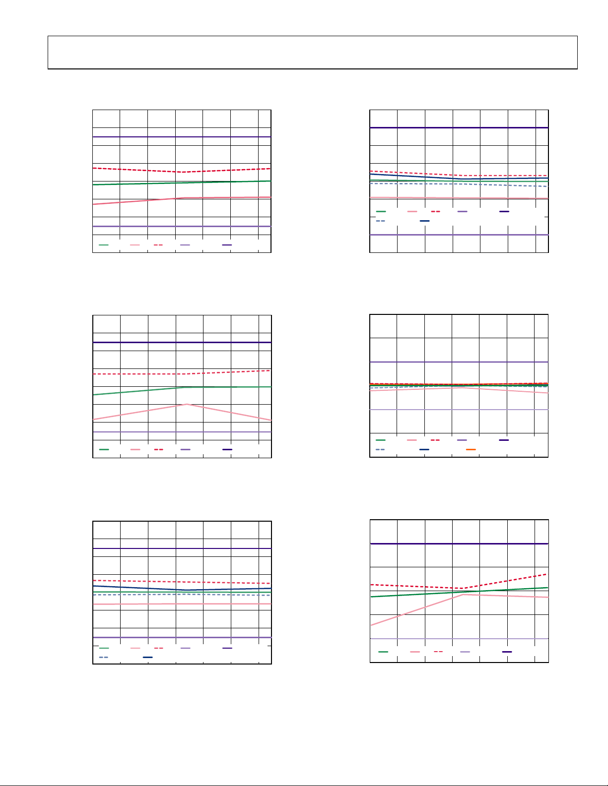
TYPICAL PERFORMANCE CHARACTERISTICS
4
3
2
1
0
–1
–2
VS1 ADC ACCURACY (%FSR)
–3
MEAN MIN MAX MIN SPE C MAX SPEC
–4
–40–200 20406080
TEMPERATURE ( °C)
08501-004
4
3
2
1
0
–1
MEAN MIN MAX MIN SPEC MAX SPEC
–2
CS1 ADC ACCURACY (%FSR)
MIN_N10% MAX_P10%
–3
–4
–40 –20 0 20 40 60 80
TEMPERATURE (°C)
Figure 4. VS1 ADC Accuracy vs. Temperature (from 10% to 90% of FSR) Figure 7. CS1 ADC Accuracy vs. Temperature (from 10% to 90% of FSR)
4
3
2
1
0
6
4
2
0
08501-007
–1
–2
VS2 ADC ACCURACY (%FSR)
–3
MEAN MIN MAX MIN SPEC MAX SPEC
–4
–40 –20 0 20 40 60 80
TEMPERATURE (°C)
08501-005
–2
CS2 ADC ACCURACY (%FSR)
–4
MEAN MIN MAX MIN SPE C MAX SPEC
MIN_P10% MAX_P10% MAX_N10%
–6
–40 –20 0 20 40 60 80
TEMPERATURE ( °C)
Figure 5. VS2 ADC Accuracy vs. Temperature (from 10% to 90% of FSR) Figure 8. CS2 ADC Accuracy vs. Temperature (from 0 mV to 200 mV)
4
3
2
1
0
–1
–2
VS3 ADC ACCURACY (%FSR)
–3
MEAN MIN MAX MIN SPEC MAX SPEC
MIN_P10% MAX_N10%
–4
–40 –20 0 20 40 60 80
TEMPERATURE (°C)
08501-006
1.35
1.30
1.25
1.20
1.15
CS1 FAST OCP THRESHOLD (V )
1.10
MEAN MIN MAX MIN SPEC MAX SPEC
1.05
–40 –20 20040608
TEMPERATURE (°C)
0
08501-008
08501-009
Figure 6. VS3 ADC Accuracy vs. Temperature (from 10% to 90% of FSR) Figure 9. CS1 Fast OCP Threshold vs. Temperature
Rev. 0 | Page 11 of 72
ADP1043A
V
THEORY OF OPERATION
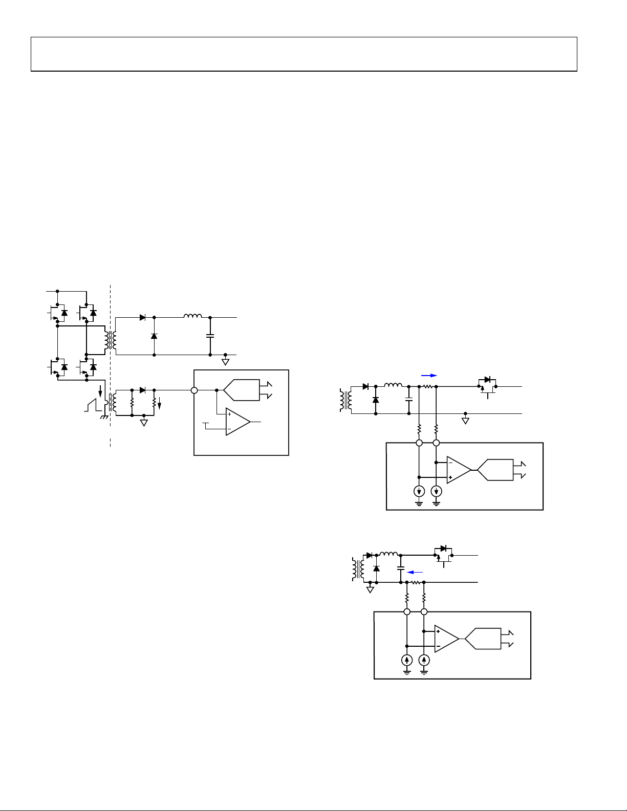
CURRENT SENSE
The ADP1043A has two individual current sense inputs: CS1
and CS2±. These inputs sense, protect, and control the output
current and the share bus information. They can be calibrated
to remove any errors due to external components.
CS1 Operation (CS1)
CS1 is typically used for the monitoring and protection of the
primary side current. This is commonly known as the current
transformer (CT) method of current sensing. The input signal
at the CS1 pin is fed into an ADC for current monitoring. The
range of the ADC is 0 V to 1.38 V. The input signal is also fed
into a comparator for fast OCP protection. The typical configuration for the current sense is shown in Figure 10.
IN
OUTA
OUTC
OUTB
OUTD
I = 10A
1kΩ 10Ω
1:100
Figure 10. Current Sense 1 (CS1) Operation
1V
I = 100mA
The comparator effectively measures peak current, and the
ADC effectively measures the average current information.
This information is available through the I
thresholds and limits can be set for CS1, such as OCP. These
thresholds and limits are described in the Current Sense and
Current Limit Registers section.
CS1
VREF
2
C interface. Various
ADC
12 BITS
FAST
OCP
CS2 Operation (CS2+, CS2−)
CS2± is used for the monitoring and protection of the secondary
side current. The full-scale range of the CS2 ADC is 225 mV. The
nominal full load voltage drop can be configured for 37.5 mV,
75 mV, or 150 mV. The differential inputs are fed into an ADC
through a pair of external resistors. When using low-side current
sensing, a 10 k resistor is required. When using high-side current
sensing, a 110 k resistor is required (for a 12 V application).
Low-side current sensing is recommended because it provides
improved performance compared with high-side current sensing.
High-side current sensing is not supported for applications
where the output voltage is above 20 V common mode. (There
is not enough offset trim range above 20 V common mode.)
Typical configurations are shown in Figure 11 and Figure 12.
Various thresholds and limits can be set for CS2, such as OCP.
These thresholds and limits are described in the Current Sense
and Current Limit Registers section.
When not in use, both CS2 inputs should be connected through
10 k resistors to PGND.
I
110kΩ 110kΩ
08501-010
1V
100µA 100µA
Figure 11. High-Side Resistive Current Sense
12V
CS2–CS2+
ADC
12 BITS
8501-011
I
10kΩ 10kΩ
CS2+CS2–
12 BITS
1V
100µA 100µA
Figure 12. Low-Side Resistive Current Sense (Recommended)
Rev. 0 | Page 12 of 72
ADC
08501-012
ADP1043A
VOLTAGE SENSE AND CONTROL LOOP
Multiple voltage sense inputs on the ADP1043A are used for the
monitoring, control, and protection of the power supply output.
The voltage information is available through the I
All voltage sense points can be calibrated digitally to remove
any errors due to external components. This calibration can be
performed in the production environment, and the settings can
be stored in the EEPROM of the ADP1043A (see the Power
Supply Calibration and Trim section for more information).
The update rate of the ADC from a control loop standpoint
is set to the switching frequency. Therefore, if the switching
frequency is set to 100 kHz, the ADC outputs a signal every
100 kHz to the control loop. Because the Σ- modulators of the
ADC sample at 1.6 MHz, the output of the ADC is the average
of the 16 readings taken during the 1.6 MHz time frame.
For voltage monitoring, the VS1, VS2, and VS3 voltage value
registers are updated every 10 ms. The ADP1043A stores every
ADC sample for 10 ms and then outputs the average value at the
end of the 10 ms period. Therefore, if these registers are read at
least every 10 ms, a true average value is read. The same applies
to the CS1 and CS2 current readings.
For the control loop, the high speed signal always comes from
the VS1 high speed ADC. The low speed signal normally comes
from the VS3 low speed ADC. However, during soft start or in
response to a load OVP or other fault condition, the ADP1043A
can switch its low speed regulating point from VS3 to VS1.
12V 12V
11kΩ11kΩ
1kΩ 1kΩ
VS2
ADCADC
VS3VS2
ADC
VS1
HIGH
SPEED
6 BITS
HIGH
FREQUENCY
FEEDBACK
LOOP
1V 1V
PGND
ADC
DIGITAL
FILTER
VS1
VS1
LOW
SPEED
12 BITS 12 BITS 12 BITS
LOW FREQUENCY
FEEDBACK LOO P
Figure 13. Voltage Sense Configuration
2
C interface.
11kΩ
VS3+
1V
1kΩ
VS3–
LOAD
12V
08501-013
VS1 Operation (VS1)
VS1 is used for the monitoring and protection of the power
supply voltage at the output of the LC stage, upstream of the
OrFET. This is also the high frequency feedback loop for the
power supply. The VS1 sense point on the power rail needs an
external resistor divider to bring the nominal common-mode
signal to 1 V at the VS1 pin (see Figure 13). The resistor divider
is necessary because the ADP1043A VS1 ADC input range is
0 V to 1.55 V. This divided-down signal is internally fed into a
high speed and a low speed Σ- ADC. The output of the VS1
ADCs goes to the digital filter.
The high speed ADC has a 2 MHz bandwidth and is run from
a 25 MHz clock. It has a range of ±18 mV. When the sampling
rate is 200 kHz, there is 0.6 mV (two LSBs) of quantization noise.
Increasing the sampling rate to 400 kHz increases the quantization noise to 1.2 mV.
In the event of a load overvoltage condition, the power supply
is regulated from the VS1 sense point, rather than from the
VS3 sense point.
VS2 Operation (VS2)
VS2 is typically used for the monitoring and protection of the
output of the power supply, downstream of the OrFET. It is
used with VS1 to control the OrFET gate drive turn-on. The
VS2 sense point on the power rail needs an external resistor
divider to bring the nominal common-mode signal to 1 V at
the VS2 pin (see Figure 13). The resistor divider is necessary
because the ADP1043A VS2 ADC input range is 0 V to 1.55 V.
This divided-down signal is internally fed into an ADC. The
output of the VS2 ADC goes to the VS2 voltage value register
(Register 0x16).
VS3 Operation (VS3+, VS3−)
VS3± is used for the monitoring and protection of the remote
load voltage. It is a fully differential input. This is the main
feedback sense point for the power supply control loop. The
VS3 sense point on the power rail needs an external resistor
divider to bring the nominal common-mode signal to 1 V at
the VS3± pins (see Figure 13). The resistor divider is necessary
because the ADP1043A VS3 ADC input range is 0 V to 1.55 V.
This divided-down signal is internally fed into an ADC. The
output of the VS3 ADC goes to the digital filter.
ADCs
The ADP1043A includes several ADCs. The high speed ADC is
described in the VS1 Operation (VS1) section. The other ADCs
are low speed, high resolution. They have a 1 kHz bandwidth
and 12-bit resolution. Each ADC has its own voltage reference
for added protection from potential failure. The digital output
of each ADC is readable through the appropriate value register.
Rev. 0 | Page 13 of 72
ADP1043A
V
DIGITAL FILTER
The loop response of the power supply can be changed using
the internal programmable digital filter. A Type 3 filter architecture has been implemented. To tailor the loop response to
the specific application, the low frequency gain, zero location,
pole location, and high frequency gain can all be set individually
(see the Digital Filter Programming Registers section). It is
recommended that the Analog Devices software GUI be used to
program the filter. The software GUI displays the filter response
in Bode plot format and can be used to calculate all stability
criteria for the power supply.
From the sensed voltage to the duty cycle, the transfer function
of the filter in z-domain is as follows:
⎛
d
⎜
=
H(z)
⎜
⎝
×
m
where:
a = filter_pole_register_value/256.
b = filter_zero_register_value/256.
c = high_frequency_gain_register_value.
d = low_frequency_gain_register_value.
m = 1 when 48.8 kHz ≤ f
m = 2 when 97.7 kHz ≤ f
SW
SW
m = 4 when 195.3 kHz ≤ f
m = 8 when 390.6 kHz ≤ f
To go from z-domain to s-domain, plug the following equation
into the H(z) equation:
sf
+
2
SW
z(s)
where
=
2
f
is the switching frequency.
SW
SW
sf
−
The digital filter introduces an extra phase delay element into
the control loop. The digital filter circuit sends the duty cycle
information to the PWM circuit at the beginning of each switching cycle (unlike an analog controller, which makes decisions on
the duty cycle information continuously). Therefore, the extra
phase delay for phase margin, Φ, introduced by the filter block is
Φ = 180 × (f
C/fSW
)
where:
f
is the crossover frequency.
C
f
is the switching frequency.
SW
At one tenth of the switching frequency, the phase delay is 18°.
The GUI incorporates this phase delay into its calculations.
Two sets of registers allow for two distinct filter responses. The
main filter, called the normal mode filter, is controlled by
programming Register 0x60 to Register 0x63. The other filter,
called the light load mode filter, is controlled by programming
Register 0x64 to Register 0x67. The ADP1043A uses the light
load mode filter only when the modulation is below the load
current threshold (programmed through Register 0x3B).
⎞
z
⎟
×
⎟
−
z
⎠
< 97.7 kHz.
< 195.3 kHz.
< 390.6 kHz.
SW
.
SW
⎛
c
⎜
⎜
68.7124.202
⎝
⎞
bz
−
⎟
×+
(1)
⎟
az
−
⎠
The Analog Devices software GUI allows the user to program
the light load mode filter in the same manner as the normal
mode filter. It is recommended that the GUI be used for this
purpose.
In addition, during the soft start process, a different set of
digital filters is used. The soft start filter value for a, b, and c in
Equation 1 is 0, and the d value is programmed through the soft
start filter gain setting (Register 0x5F[1:0]).
PWM AND SYNC RECT OUTPUTS (OUTA, OUTB, OUTC, OUTD, OUTAUX, SR1, SR2)
The PWM and SR outputs are used for control of the primary
side drivers and the synchronous rectifier drivers. These outputs
can be used for several control topologies, including full-bridge,
phase-shifted ZVS, and interleaved two switch forward converter
configurations. Delays between rising and falling edges can be
individually programmed. Special care must be taken to avoid
shoot-through and cross-conduction. It is recommended that
the Analog Devices software GUI be used to program these
outputs. Figure 14 shows an example configuration to drive a
full-bridge, phase shift topology with synchronous rectification.
IN
OUTA OUTC
SR2
SR2
08501-014
SR1
OUTB OUTD
DRIVER
SR1
OUTA
DRIVER
ADuM1410
Figure 14. PWM Pin Assignment
OUTB
OUTC
OUTD
The PWM and SR outputs all work together. Therefore, when
reprogramming more than one of these outputs, it is important to
first update all the registers, and then latch the information into
the ADP1043A at one time. During reprogramming, the outputs
are temporarily disabled. A special instruction is sent to the
ADP1043A to ensure that new timing information is programmed
simultaneously. This is done by setting Register 0x5D[0] to 1. It is
recommended that PWM outputs be disabled when not in use.
OUTAUX is an additional PWM output pin; OUTAUX allows
an extra PWM signal to be generated at a different frequency
from the other six PWM outputs. This signal can be used to
drive an extra power converter stage, such as a buck controller
located in front of a full-bridge converter. OUTAUX can also be
used as a clock reference signal.
Rev. 0 | Page 14 of 72
ADP1043A
SYNCHRONOUS RECTIFICATION
SR1 and SR2 are recommended for use as the PWM control
signals when using synchronous rectification. These PWM
signals can be set up similarly to the other PWM outputs. The
turn-on of these signals can be programmed in two ways. They
can either be turned on to their full PWM value immediately, or
they can be turned on in a soft start fashion. When turned on
in a soft start, the signals ramp up from zero duty cycle to the
desired duty cycle. The advantage of ramping the SR signals is
to minimize a voltage step that would occur by turning the SR
FETs on completely. The advantage of turning the SR signals
completely on immediately is that they can help to minimize
the voltage transient caused by a load step.
Using Register 0x54[1], the SR soft start can be programmed to
occur just once, the first time that the SR signals are enabled, or
every time that the SR signals are enabled.
When programming the ADP1043A to use SR soft start, ensure
correct operation of this function by setting the falling edge of
) to a lower value than the rising edge of SR1 (t9) and by
SR1 (t
10
setting the falling edge of SR2 (t
rising edge of SR2 (t
).
11
) to a lower value than the
12
The speed of the SR enable is approximately 200 s. This ensures
that in case of a load step, the SR signals (and any other PWM
outputs that are temporarily disabled) can be turned on quickly
enough to prevent damage to the FETs that they are controlling.
ADAPTIVE DEAD TIME CONTROL
A set of registers called the adaptive dead time (ADT) registers
(Register 0x68 to Register 0x6F) allows the dead time between
PWM edges to be adapted on-the-fly. The ADP1043A uses the
ADT only when the modulation is below the dead time (load
current) threshold (programmed in Register 0x68). The Analog
Devices software GUI allows the user to easily program the
dead time values, and it is recommended that the software be
used for that purpose.
Each individual PWM rising and falling edge (t
to t14) can then
1
be programmed to have a specific dead time offset. This offset
can be positive or negative. The offset is relative to the nominal
edge position. For example, if t
100 ns and the ADT setting for t
has a nominal rising edge of
1
is −15 ns, t1 moves to 85 ns
1
when it falls below the adaptive dead time threshold. The dead
times are programmed using Register 0x69 to Register 0x6F.
LIGHT LOAD MODE
Register 0x3B allows the ADP1043A to shut down PWM
outputs under light load conditions. The light load current
threshold can be programmed. Below this current threshold,
the SR outputs are disabled. The user can also program any of
the other PWM outputs to shut down below this current threshold. This allows the ADP1043A to be used with an interleaved
two transistor forward topology, incorporating phase shedding
at light load. The light load mode digital filter is also used
during light load mode.
Rev. 0 | Page 15 of 72
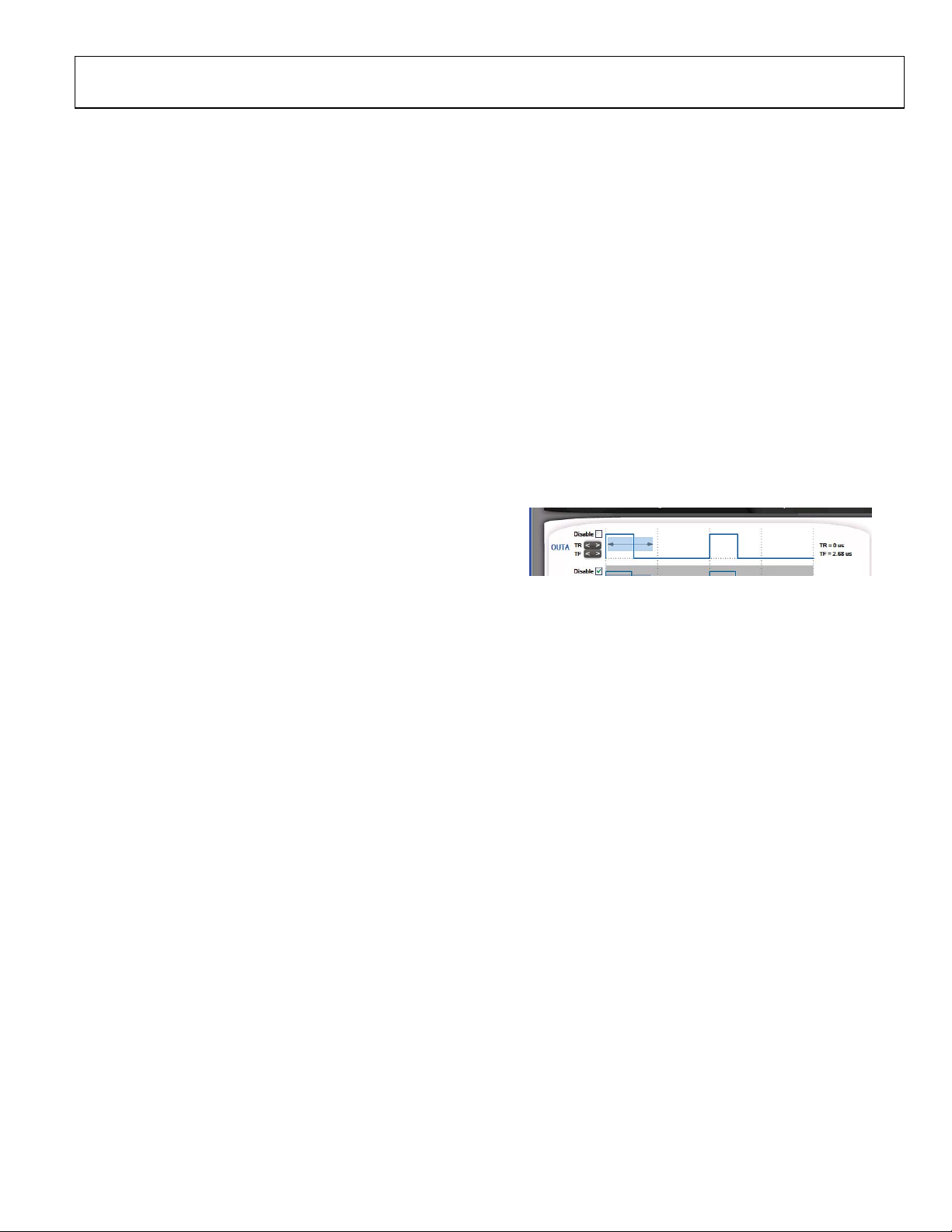
MODULATION LIMIT
Using the modulation limit register (Register 0x2E), it is possible to
apply a maximum modulation limit and a minimum modulation
limit to any PWM signal, thus limiting the modulation range of
any PWM. These limits are a percentage of the switching period.
If the modulation required is lower than the minimum setting,
pulse skipping can be enabled.
Following is an example of how to use the modulation limit
settings. In this example, the switching cycle period is 4 s
and modulation on the t
nominal position of t
edge (falling edge) is enabled. The
2
is set to 1.6 s, which is 40% of the 4 s
2
period. The modulation high limit is set to (nominal + 50%).
Therefore, the modulation high limit is (40% + 50%) = 90% of
the switching cycle period; 90% of 4 s = 3.6 s. The modulation
low limit is set to (nominal − 35%). Therefore, the modulation
low limit is (40% − 35%) = 5% of the switching cycle period;
5% of 4 s = 0.2 s.
The GUI provided with the ADP1043A is recommended for
evaluating this feature of the ADP1043A (see Figure 15).
8501-015
Figure 15. Setting Modulation Limits (Modulation Range Shown by Arrows)
OrFET CONTROL (GATE)
The GATE control signal drives an external OrFET. The OrFET
gate control is used to protect against power flow into the power
supply from another supply. This ensures that power flows only
out of the power supply and that the unit can be hot-swapped.
The OrFET circuit can be used only when the ADP1043A is
connected to a sense resistor on the low side. The OrFET circuit
is not guaranteed for operation with high-side current sensing.
The GATE pin is an open-drain, N-channel MOSFET. An
external 2.2 kΩ pull-up resistor is recommended. Its output is
normally high to keep the OrFET turned off. When the start-up
criteria have been achieved, the GATE output is pulled low,
allowing the OrFET to turn on. The OrFET turn-on and turnoff thresholds can be individually programmed. The GATE
outputs are CMOS levels (0 V to 3.3 V). An external driver is
required to turn the OrFET on or off.
The OrFET can be turned off by three methods:
Fault flag (any fault flag can be programmed to turn off the
•
OrFET)
•
Fast OrFET control circuit
•
Accurate OrFET control circuit
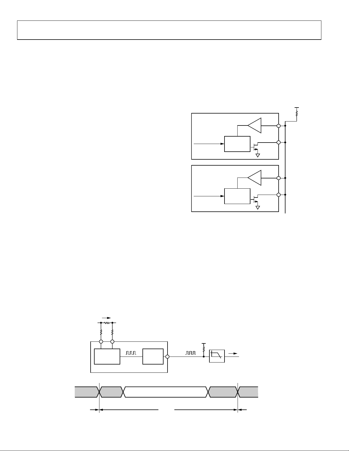
Fast OrFET control looks at the reverse voltage across CS2+
and CS2− and is implemented using an analog comparator
(see Figure 16). If the voltage difference between CS2+ and
CS2− is greater than the fast OrFET threshold programmed
in Register 0x30, the OrFET is turned off.
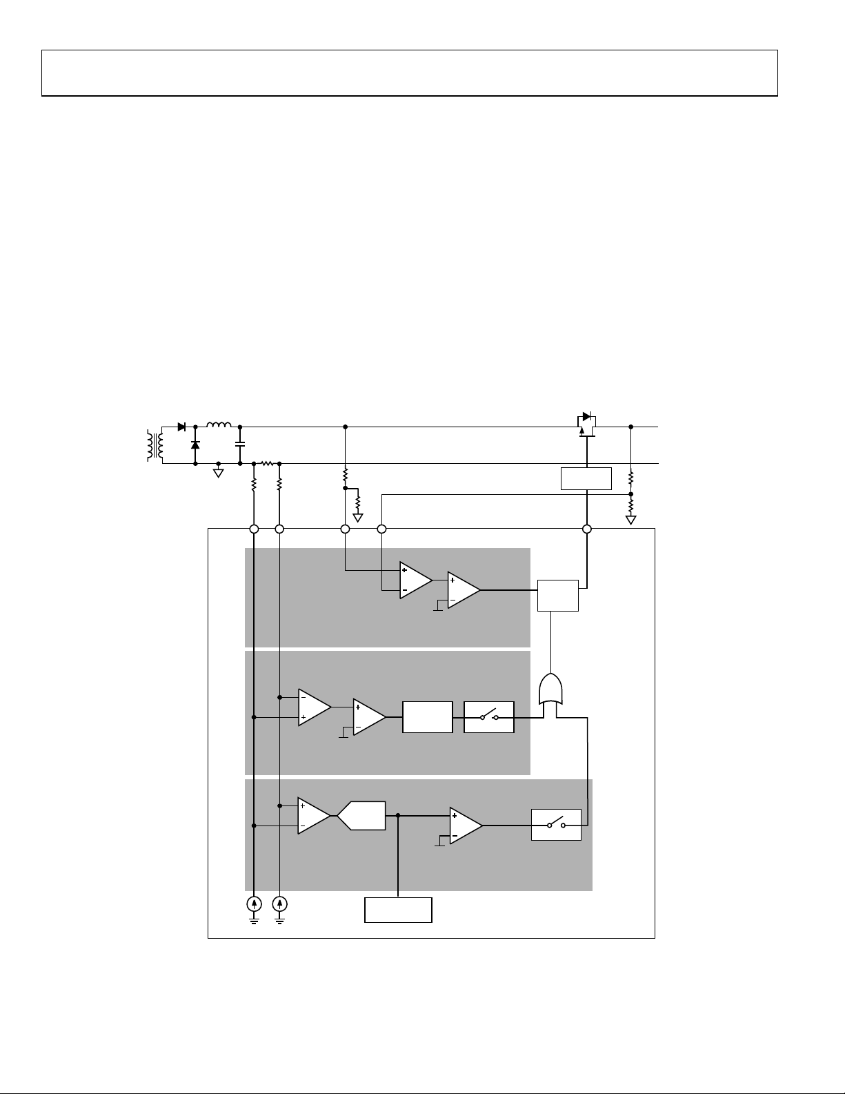
ADP1043A
Accurate OrFET control also uses the reverse voltage across the
CS2+ and CS2− pins to disable the OrFET (see Figure 16). If the
voltage difference between CS2+ and CS2− is greater than 0 mV,
the OrFET is disabled. The accurate OrFET circuit is more accurate, but it is slower than the fast OrFET circuit.
The OrFET turn-on circuit looks at the voltage difference
between VS1 and VS2 (see Figure 16). When the forward
voltage drop from VS1 to VS2 is greater than the programmable OrFET enable threshold (Register 0x30[5:4]), the
OrFET is enabled. The OrFET enable threshold can be set to
−0.5%, 0%, 1%, or 2% of the nominal output voltage (12 V).
R
SENSE
10kΩ 10kΩ
11kΩ
1kΩ
Recommended Setup
In a 12 V application, while in normal operating mode
When 12 V < V
•
< OVP, use the accurate OrFET control
OUT
circuit to turn off the OrFET.
•
When V
> OVP, use load OVP to turn off the OrFET.
OUT
In a 12 V application, while in light load mode
When 12 V < V
•
< OVP, use ACSNS to turn off the
OUT
OrFET.
•
When V
> OVP, use load OVP to turn off the OrFET.
OUT
In a 12 V application, when an internal short circuit occurs,
follow this procedure:
1.
Use fast OrFET to turn off the OrFET.
Use CS1 OCP or VS1 UVP to shut down the unit and
2.
restart it.
12V
V
OUT
DRIVER
11kΩ
1kΩ
CS2– VS1 VS2CS2+
DIFFERENTIAL
TO SINGLE-
ENDED
DIFFERENTIAL
TO SINGLE-
ENDED
100µA 100µA
Figure 16. OrFET Control Circuit Internal Detailed Diagram
FAST OrFET
COMPARATOR
FAST OrFET
THRESHOLD
REG 0x30[3:2]
CS2 ADC
OrFET ENABLE
THRESHOLD
REG 0x30[5:4]
FAST OrFET
DEBOUNCE
REG 0x30[1]
ACCURATE OrFET
REG 0x30[7:6]
CS2 VALUE
REGISTER
REG 0x18[15:4]
THRESHOLD
OrFET
ENABLE
FAST OrFET
BYPASS
REG 0x30[0]
ACCURATE
OrFET
DISABLE
FLAG
SRQ
OrFET
DISABLE
FLAGS
GATE
08501-016
Rev. 0 | Page 16 of 72
ADP1043A
OrFET Operation Examples
Hot Plug into a Live Bus
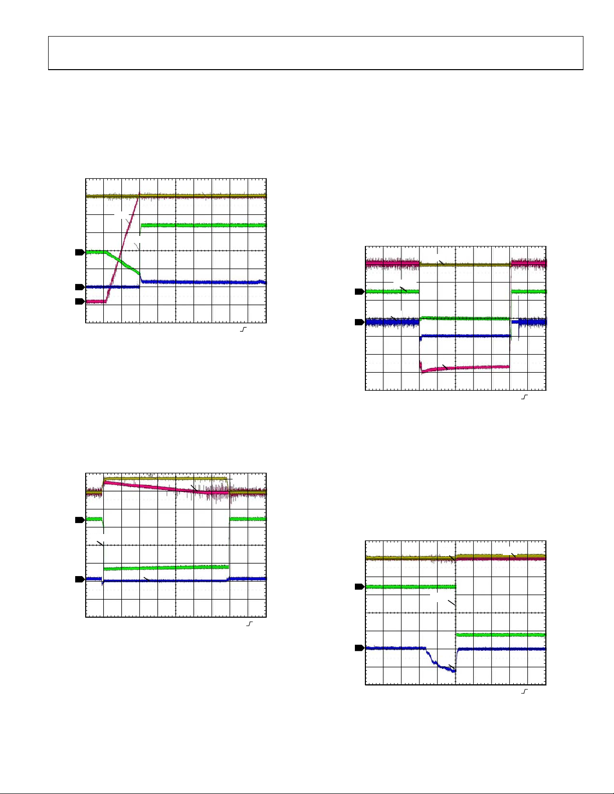
A new PSU is plugged into a live 12 V bus (yellow). The internal
voltage VS1 (red) is ramped up before the OrFET is turned on.
After the OrFET is turned on (green), current in the new PSU
begins to flow to the load (blue). The turn-on voltage threshold
between the new PSU and the bus is programmable.
VS3
VS1
OrFET
4
Short Circuit
When one of the output rectifiers fails, the bus voltage can
collapse if the OrFET is not promptly turned off. The fast
OrFET comparator is used to protect the system from this fault
event. Figure 19 shows a short circuit applied to the output
capacitors, before the OrFET. After the fast OrFET threshold for
CS2 (blue) is triggered, the OrFET (green) is turned off. In this
case, the gate driver is not very fast and takes about 500 ns. (A
larger buffer to drive the OrFET would turn it off quicker.)
Figure 19 also shows the operation when the short circuit is
removed. The internal regulation point, VS1 (red), returns to
12 V, and the OrFET (green) is reenabled. The PSU again begins
to contribute current to the load (blue).
VS3
3
2
CH1 2.00V
CH3 2.00A
CS2
CH2 2.00V
CH4 10.0V
M10.0ms A CH4 100mV
08501-017
Figure 17. Hot Plug into a Live Bus (Yellow Is Bus Voltage; Red Is VS1 Voltage;
Green Is OrFET Control Signal; Blue Is Load Current)
Runaway Master
A rogue PSU on the bus (yellow) has a fault condition, and the
result is that the bus voltage increases above the OVP threshold.
The good PSU turns off the OrFET (green) and regulates its
internal voltage VS1 (red). When the rogue power supply fault
condition is removed, the bus voltage decreases. The OrFET of
the good PSU is immediately turned on and the good PSU
resumes regulating from VS3.
VS1
4
OrFET
VS3
CS2
CH1 2.00V
CH3 2.00A
OrFET
CH2 2.00V
CH4 10.0V
VS1
M200.0ms A CH4 7.5mV
08501-019
4
3
Figure 19. Internal Short Circuit (Yellow Is Bus Voltage; Red Is VS1 Voltage;
Green Is OrFET Control Signal; Blue Is Load Current)
Light Load Mode Operation
PSU 1 increases its voltage at light load from 12 V to 12.1 V
(yellow). Both PSU 1 and PSU 2 are CCM, so PSU 1 sources
current and PSU 2 sinks current (blue). In PSU 2, after 10 ms
the accurate OrFET control turns off the OrFET to prevent
reverse current from flowing. Note that the OrFET voltage
(green) is solid during this transition because PSU 1 and PSU 2
are in CCM mode.
VS1
VS3
3
CH1 2.00V
CH3 2.00A
CS2
CH2 2.00V
CH4 10.0V
M50.0ms A CH4 0mV
Figure 18. Runaway Master (Yellow Is Bus Voltage; Red Is VS1 Voltage;
Green Is OrFET Control Signal; Blue Is Load Current)
08501-018
Rev. 0 | Page 17 of 72
4
OrFET
3
CS2
CH1 2.00V
CH3 2.00A
CH2 2.00V
CH4 10.0V
M5.0ms A CH4 8.3mV
Figure 20. Light Load Mode (Yellow Is Bus Voltage; Red Is VS1 Voltage;
Green Is OrFET Control Signal; Blue Is Load Current)
08501-020

ADP1043A
VDD
When VDD is applied, a certain time elapses before the part is
capable of regulating the power supply. When the VDD rises
above the power-on reset and UVLO levels, it takes approximately 20 s for VCORE to reach its operational point of 2.5 V.
The EEPROM contents are then downloaded to the registers.
The download takes an additional 25 s (approximately). After
the EEPROM download, the ADP1043A is ready for operation.
If the ADP1043A is programmed to power up at this time, the
soft start ramp begins.
VDD/VCORE OVLO
The ADP1043A has built-in overvoltage protection (OVP) on
its supply rails. When the VDD or VCORE voltage rises above
the OVLO threshold, the response can be programmed. This
circuit can be set to be ignored, but it is recommended that the
user not program the OVP circuit to be ignored.
POWER GOOD
The ADP1043A has two power-good pins. The PGOOD1 pin
and fault flag are set when any of the following conditions are
out of range: power supply, CS1 fast OCP, CS1 accurate OCP,
CS2 accurate OCP, UVP, local OVP, or load OVP.
The PGOOD2 pin and fault flag are set when any flag is set:
power supply, OrFET, CS1 fast OCP, CS1 accurate OCP, CS2
accurate OCP, voltage continuity, UVP, accurate OrFET disable,
ACSNS, external flag (FLAGIN), VCORE OV, VDD OV, local
OVP, load OVP, OTP, CRC fault, and EEPROM unlocked.
If Register 0x2D[3] is set, PGOOD2 looks only at the flags that
are not programmed to be ignored.
The PGOOD2 pin can also be used as an interrupt pin to notify
a host controller that a flag has been set. The polarity of the
PGOOD1 and PGOOD2 pins is configured as active low.
Rev. 0 | Page 18 of 72
ADP1043A
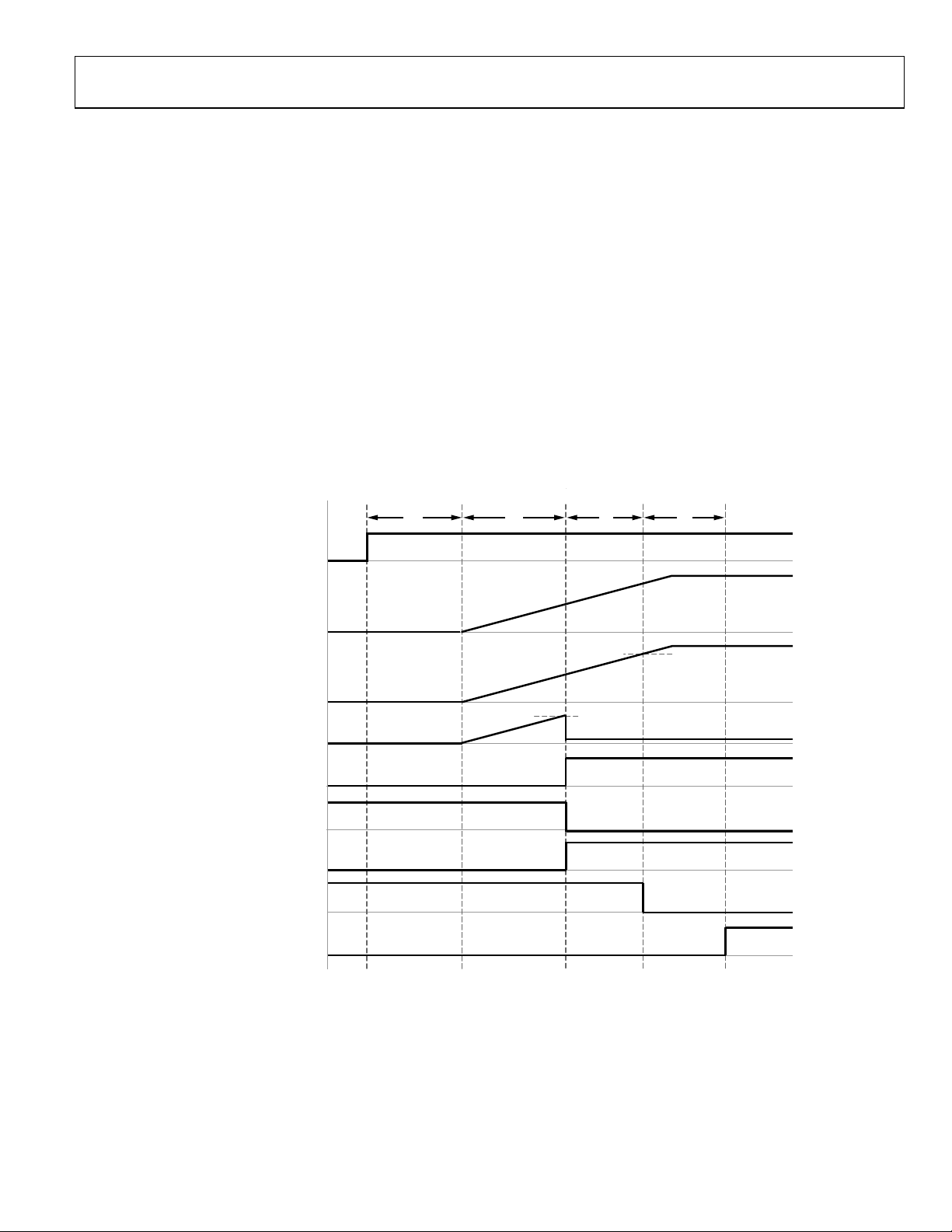
The soft start begins to ramp up the power supply voltage
SOFT START
A dedicated filter is used during soft start. The filter is disabled
at the end of the soft start routine, and the voltage loop digital
filter is used.
Fault Condition During Soft Start
If a CS1 fast OCP fault condition occurs during soft start, the
entire soft start routine is reset, and the ADP1043A begins another
soft start routine. All other fault flags are ignored during soft start.
Soft Start Routine
When the user turns on the power supply (enables PSON), the
following soft start procedure occurs:
1.
The PSON signal is enabled at Time t
checks that initial flags are OK. These flags include VDD
OK and GND OK.
The ADP1043A waits for Time t
2.
The length of t
is set in Register 0x2C, Bits[4:3].
1
. The ADP1043A
0
before it begins soft start.
1
t
0
t
1
3.
at the start of Time t
The ADP1043A keeps the OrFET gate signal turned off.
4.
.
2
The voltage differential across the OrFET increases (VS1 −
VS2) due to the diode conduction of the OrFET. When the
voltage differential reaches the OrFET enable threshold
(Register 0x30, Bits[5:4]), the OrFET gate signal is enabled
at Time t
. The ADP1043A begins to regulate voltage from
3
VS3 instead of VS1.
After the power supply voltage increases above the VS1 UVP
5.
undervoltage limit (Register 0x34, Bits[6:0]), at the end of
, the UVP flag is reset.
Time t
4
After the UVP flag is reset and if all other PGOOD1 fault
6.
conditions are OK, the PGOOD1 signal waits for Time t
before it is enabled. The length of t
is programmable in
5
Register 0x2D, Bits[7:4].
t
3
t
2
t
4
t
5
5
PSON
SOFT START RAMP
V
VOLTAGE
OUT
(VS1 – VS2) VOLTAGE
GATE SIGNAL
LOOP CO NTROLLED FROM VS1
LOOP CO NTROLLED FROM VS3
UVP FLAG
PGOOD1
120mV
Figure 21. Soft Start Timing Diagram
UVP
08501-021
Rev. 0 | Page 19 of 72
ADP1043A
V
CURRENT SHARING (SHARE)
The ADP1043A supports both analog current sharing and
digital current sharing. It is recommended that analog current
sharing be used because it offers improved performance over
digital current sharing. Digital current sharing requires a load
line of >15 mΩ to prevent oscillation between units. The analog
current sharing scheme has no such issues.
Using Register 0x29, Bit 3, it is possible to program the
ADP1043A to use the CS1 current information or the CS2
current information for current sharing.
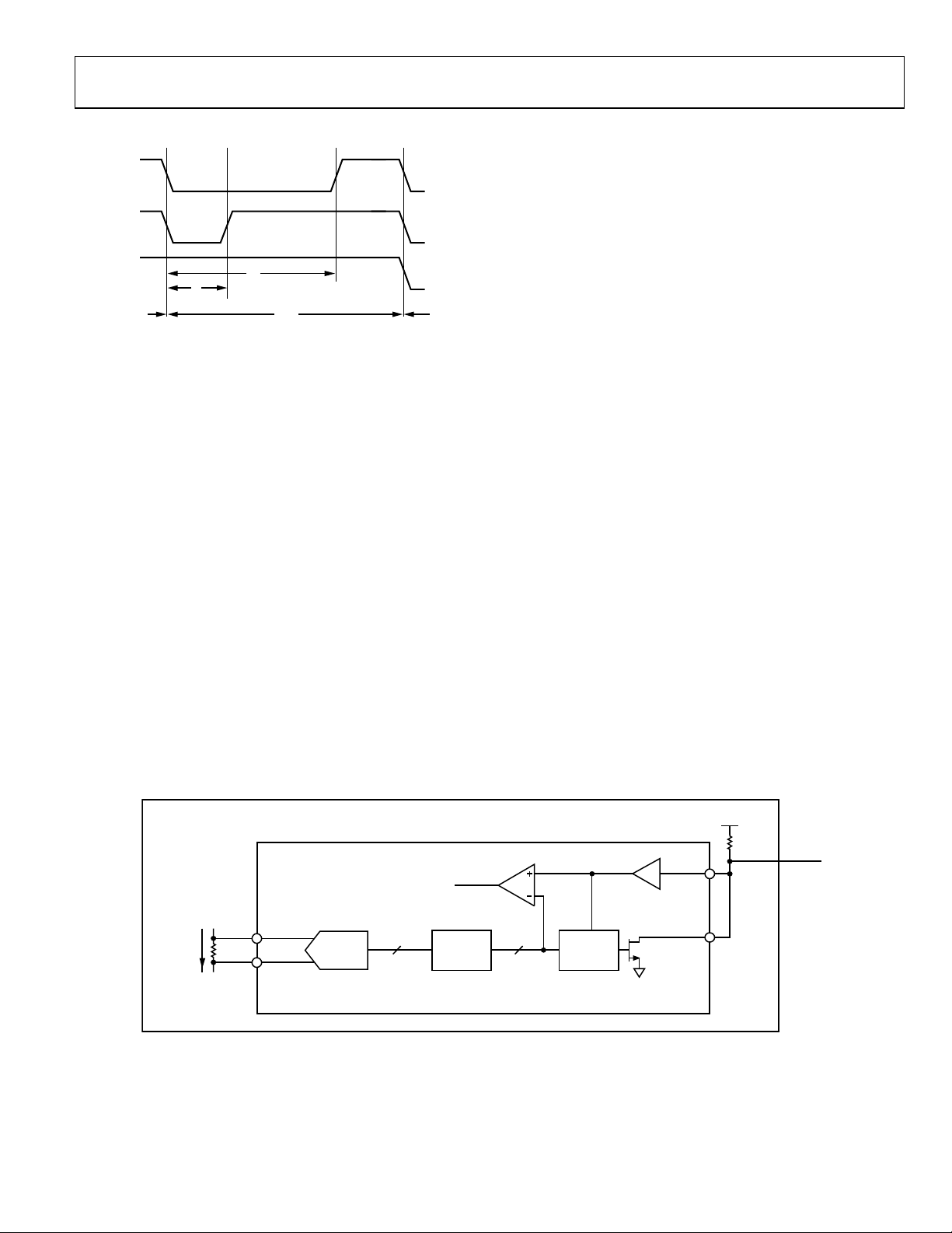
Analog Current Sharing
The ADP1043A supports analog current sharing. The current
reading from CS1 or CS2 can be output to the SHAREo pin in
the form of a digital bit stream, which is the output of the current
sense ADC (see Figure 23). The bit stream is proportional to the
current being delivered by this unit to the load. By filtering this
digital bit stream using an external RC filter, the current information is turned into an analog voltage. This means that there is
now an analog voltage that is proportional to the current being
delivered by this unit to the load. This voltage can be compared
to the share bus. If the unit is not supplying enough current, an
error signal can be applied to the VS3 feedback point. This signal
causes the unit to increase its output voltage and, therefore, its
current contribution to the load.
For more information about the analog current share functionality, including schematics and measurements in different fault
and setup conditions, see the product page for the ADP1043A.
Digital Share Bus
The digital share bus scheme is similar in principle to the traditional analog share bus scheme. The difference is that instead of
using a voltage on the share bus to represent current, a digital
word is used.
The ADP1043A outputs a digital word onto the share bus. The
digital word is a function of the current that the power supply is
providing (the higher the current, the larger the digital word).
CURRENT
The power supply with the highest current controls the bus
(master). A power supply that is putting out less current (slave)
sees that another supply is providing more power to the load
than it is. During the next cycle, the slave increases its current
output contribution by increasing its output voltage. This cycle
continues until the slave outputs the same current as the master,
within a programmable tolerance range. Figure 22 shows the
configuration of the digital share bus.
DD
SHAREi
CURRENT SENSE
INFO
POWER SUPPLY A
CURRENT SENSE
INFO
POWER SUPPLY B
DIGITAL
WORD
DIGITAL
WORD
SHAREo
SHAREi
SHAREo
SHARE
BUS
08501-023
Figure 22. Digital Current Share Configuration
The digital share bus is based on a single-wire communication
bus principle; that is, the clock and data signals are contained
together.
When two or more ADP1043A devices are connected, they
synchronize their share bus timing. This synchronization is
performed by the start bit at the beginning of a communications
frame. If a new ADP1043A is hot-swapped onto an existing
digital share bus, it waits to begin sharing until the next frame.
The new ADP1043A monitors the share bus until it sees a stop
bit, which designates the end of a share frame. It then performs
synchronization with the other ADP1043A devices during the
next start bit. The digital share bus frame is shown in Figure 24.
CS2–CS2+
LPF
VOLTAGE
08501-022
CURRENT
SENSE
ADC
SHARE
BIT STREAM BIT STREAM
BUS
SHAREo
Figure 23. Analog Current Share Configuration
2 STOP BI TS
(IDLE)
PREVIOUS
FRAME
START BIT
0
8-BIT DATA
FRAME
Figure 24. Digital Current Share Frame Timing Diagram
Rev. 0 | Page 20 of 72
2 STOP BIT S
(IDLE)
START BIT
0
NEXT FRAME
8501-024
ADP1043A
Figure 25 shows the possible signals on the share bus.
LOGIC 1
LOGIC 0
IDLE
PREVIOUS
BIT
t
0
t
1
NEXT
t
BIT
BIT
08501-025
Figure 25. Share Bus High, Low, and Idle Bits
The length of a bit (t
) is fixed at 10 s. A Logic 1 is defined as
BIT
a high-to-low transition at the start of the bit and a low-to-high
transition at 75% of t
. A Logic 0 is defined as a high-to-low
BIT
transition at the start of the bit and a low-to-high transition at
25% of t
The bus is idle when it is high during the whole period of t
All other activity on the bus is illegal. Glitches up to t
BIT
.
.
BIT
GLITCH
(200 ns) are ignored.
The digital word that represents the current information is eight
bits long. The ADP1043A takes the eight MSBs of the CS1 or CS2
reading (whichever the user chooses as the current share signal)
and uses this reading as the digital word. When read, the share
bus value at any given time is equal to the CS1 or CS2 current
reading (see Figure 26).
Digital Share Bus Scheme
Each power supply compares the digital word that it is outputting
with the digital words of all the other supplies on the bus.
Round 1
In Round 1, every supply first places its MSB on the bus. If a
supply senses that its MSB is the same as the value on the bus, it
continues to Round 2. If a supply senses that its MSB is less than
the value on the bus, it means that this supply must be a slave.
When a supply becomes a slave, it stops communicating on the
share bus because it knows that it is not the master. The supply
then increases its output voltage in an attempt to share more
current.
If two units have the same MSB, they both continue to Round 2,
because either of them could be the master.
Round 2
In Round 2, all supplies that are still communicating on the bus
place their second MSB on the share bus. If a supply senses that
its MSB is less than the value on the bus, it means that this
supply must be a slave and it stops communicating.
Round 3 to Round 8
The same algorithm is repeated for up to eight rounds to allow
supplies to compare their digital words and, in this way, to
determine whether each unit is the master or a slave.
Digital Share Bus Configuration
The digital share bus can be configured in various ways.
The bandwidth of the share bus loop is programmable in
Register 0x29[2:0]. The extent to which a slave tries to match
the current of the master can be selected by programming
Register 0x2A[3:0]. The primary side or the secondary side
can be used as the current share signal by programming
Register 0x29[3].
A load line may be required between PSUs when using a digital
share bus. A minimum impedance of 15 m is recommended
between the remote voltage sense node and the load.
I
OUT
= 35A
1mΩ
CS2+
CS2–
+
35mV
–
15.26µV = 1 LSB
CURRENT
SENSE
ADC
12-BIT
2293 DEC
0x8F5
PSU A
MASTER
DIGITAL
FILTER
÷16
35mV/15.26µ V = 229 3
8-BIT
143 DEC
0x8F
DIGITAL
WORD
0x8F
0x8F
SHAREi
SHAREo
8-BIT
WORD
V
DD
SHARE
BUS
8-BIT
WORD
0x8F
8501-026
Figure 26. How the Share Bus Generates the Digital Word to Place on the Digital Share Bus
Rev. 0 | Page 21 of 72
ADP1043A
POWER SUPPLY SYSTEM AND FAULT MONITORING
The ADP1043A has extensive system and fault monitoring
capabilities. The system monitoring functions include voltage,
current, power, and temperature readings. The fault conditions
include out-of-limit values for current, voltage, power, and temperature. The limits for the fault conditions are programmable.
The ADP1043A has an extensive set of flags that are set when
certain thresholds or limits are exceeded. These thresholds and
limits are described in the Fault Registers section.
FLAGS
The ADP1043A has an extensive set of flags that are set when
certain limits, conditions, and thresholds are exceeded. The
real-time status of these flags can be read in Register 0x00 to
Register 0x03. The response to these flags is individually
programmable. Flags can be ignored or used to trigger tasks
such as turning off certain PWM outputs or the OrFET GATE
output. Flags can also be used to turn off the power supply. The
ADP1043A can be programmed to respond when these flags are
reset. For more information, see Register 0x08 to Register 0x0D.
The ADP1043A also has a set of latched fault registers
(Register 0x04 to Register 0x07). The latched fault registers
have the same flags as Register 0x00 to Register 0x03, but the
flags in the latched registers remain set so that intermittent
faults can be detected. Reading a latched register resets all the
flags in that register.
MONITORING FUNCTIONS
The ADP1043A monitors and reports several signals, including
voltages, currents, power, and temperature. All these values are
2
stored in individual registers and can be read through the I
C
interface. See the Value Registers section for more details.
VOLTAGE READINGS
The VS1, VS2, and VS3 ADCs have an input range of 1.55 V.
The outputs of the ADCs are 12-bit values, which means that
the LSB size is 1.55 V/4096 = 378.4 V. The user is limited to an
input range of 1.5 V, which means that the ADC output code is
limited to 1.5 V/378.4 V = 3964.
The equation to calculate the ADC code at a certain voltage
(Vx) is given by the following formula:
ADC Code = Vx/378.4 V
For example, when there is 1 V on the input of the ADC
ADC Code = 1 V/378.4 V
ADC Code = 2643
In a 12 V application, the 12 V reading is divided down using
a resistor divider network to provide 1 V at the sense pin.
Therefore, to convert the register value to a real voltage, use
the following formula:
V
= (VSx_Voltage_Value/2643) × ((R1 + R2)/R2)
OUT
Rev. 0 | Page 22 of 72
In a 12 V system, this equates to
V
= (VSx_Voltage_Value/2643) × 12 V
OUT
CURRENT READINGS
CS1 Pin
DC Input Voltage
The CS1 ADC is identical in design to the VS1, VS2, and VS3
ADCs. Therefore, the description in the Vo lt a ge Re ad i ng s section
also applies to the CS1 ADC. When there is exactly 1 V on the
CS1 pin, the value in the CS1 value register (Register 0x13)
reads 2968.
CS1 has an input range of 1.38 V. The ADC performs a 12-bit
reading conversion on this value, which means that the LSB size
is 1.38 V/4096 = 337 V.
The equation to calculate the ADC code at a certain CS1 input
voltage (Vx) is given by the following formula:
ADC Code = Vx/337 V
For example, when there is 1 V on the CS1 input pin
ADC Code = 1 V/337 V
ADC Code = 2968
AC Input Voltage
CS1 often receives a rectified ac signal through a current
transformer. In this case, the ADC has a frequency response
(see Figure 27).
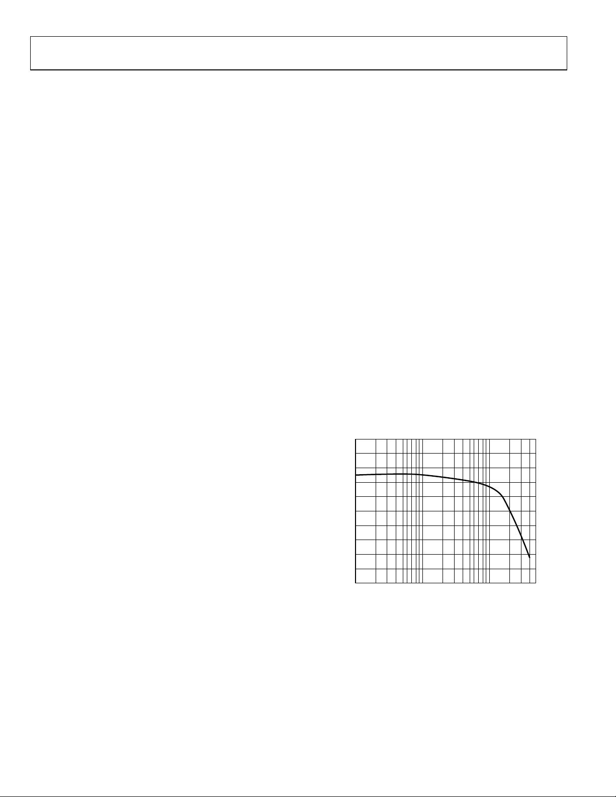
105
103
101
99
97
95
93
91
PERCENTAGE DEV IATION (%)
89
CS1 ADC FREQUENCY RESP ONSE
87
85
1k 10k 100k
To compensate for this frequency response, the multiplication
factor (M) should be used, as shown in the following equation:
M = (−2 × 10
where
−18
× f
f
is the switching frequency of the power supply.
SW
Using the multiplication factor (M) results in a more accurate
reading. This formula can be used by an MCU or other system
monitoring device. The ADP1043A GUI has the option to use
this formula.
CS1 INPUT FREQUENCY ( Hz)
Figure 27. CS1 ADC Frequency Response
3
) + (2 × 10
SW
−12
2
× f
) + (2 × 10⁻⁸ × fSW) + 0.9998
SW
08501-041

ADP1043A
Ω
CS2 Pin
The user sets the full-scale (FS) voltage drop—37.5 mV,
75 mV, or 150 mV—that is present across the R
SENSE
resistor
by programming Register 0x23, Bits[7:6].
The CS2 ADC has an input range of 250 mV. The resolution is
12 bits, which means that the LSB size is 250 mV/4096 = 61.04 V.
The user is limited to an input range of 215 mV.
The equation to calculate the ADC code at a certain voltage
) is given by the following formula:
(V
X
ADC Code = V
/250 mV × 4096
X
For example, when there is 150 mV on the input of the ADC
ADC Code = 150 mV/250 mV × 4096
ADC Code = 2457
Therefore, to convert the CS2 value reading to a real current,
use the following formula:
I
= (CS2_Value/2457) × (FS/R
OUT
SENSE
)
where:
FS is the full-scale voltage drop (37.5 mV, 75 mV, or 150 mV).
R
is the sense resistor value.
SENSE
For example, if CS2_Value = 1520, R
= 20 mΩ, and
SENSE
FS = 150 mV, the real current is calculated as follows:
I
= (1520/2457) × (150 mV/20 mΩ)
OUT
I
= 4.64 A
OUT
POWER READINGS
The output power value register (Register 0x19) is the product
of the VS3 voltage value and the CS2 current value. Therefore,
a combination of the formulas in the Vol ta ge Re ad in gs section
and the CS2 Pin section is used to calculate the power reading
in watts. This register is a 16-bit word. It multiplies two 12-bit
numbers and discards the eight LSBs.
P
= (V
OUT
OUT
) × (I
OUT
)
For example,
P
= (12 V) × (4.64 A) = 55.68 W
OUT
POWER MONITORING ACCURACY
The ADP1043A power monitoring accuracy is specified relative
to the full-scale range of the signal that it is measuring.
FIRST FLAG FAULT ID AND VALUE REGISTERS
When the ADP1043A registers several fault conditions, it stores
the value of the first fault in a dedicated register. For example, if
the overtemperature (OTP) fault is registered, followed by an
OVP fault, the OTP flag is stored in the first flag ID register
(Register 0x10). This register gives the user more information
for fault diagnosis than a simple flag. The contents of this register
are latched, meaning that they are stored until read by the user.
The contents are also reset by a PSON signal.
If a flag is set to be ignored, it does not appear in the first flag
register.
EXTERNAL FLAG INPUT (FLAGIN PIN)
The FLAGIN pin can be used to send an external fault
signal into the ADP1043A. The reaction to this flag can
be programmed in the same way as the internal flags.
TEMPERATURE READINGS (RTD PIN)
The RTD pin is set up for use with an external 100 kΩ negative
temperature coefficient (NTC) thermistor. The RTD pin has an
internal 10.8 A current source. Therefore, with a 100 kΩ thermistor, the voltage on the RTD pin is 1 V at 25°C. An ADC on the
ADP1043A monitors the voltage on the RTD pin.
10µA
100k
NTC
RTD
RTD TEMPERAT URE
VALUE REGISTER
REG 0x1A[15:4]
RTD
ADC
OTP
THRESHOLD
REG 0x2F[7:0]
Figure 28. RTD Pin Internal Details
OTP
FLAG
FLAGS
The output of the RTD ADC is linearly proportional to the
voltage on the RTD pin. However, thermistors exhibit a nonlinear function of resistance vs. temperature. Therefore, it is
necessary to perform some postprocessing on the RTD ADC
reading to accurately read the temperature. This postprocessing
can be in the form of a lookup table or polynomial equation to
match the specific NTC being used.
OVERTEMPERATURE PROTECTION (OTP)
If the temperature sensed at the RTD pin exceeds the programmable threshold, the OTP flag is set. The hysteresis on this flag
is 16 mV (see Register 0x2F in Table 4 3 for details). The response
to the OTP flag is programmable.
The RTD trim is required to make accurate temperature readings
at the lower end of the RTD ADC range. This results in a more
accurate measurement for determining the OTP threshold (see
the RTD/OTP Trim section).
08501-027
Rev. 0 | Page 23 of 72

ADP1043A
V
OVERCURRENT PROTECTION (OCP)
The ADP1043A has several OCP functions. CS1 and CS2 have
individual OCP circuits to provide both primary and secondary
side protection.
CS1 has two protection circuits: CS1 fast OCP and CS1 accurate
OCP (see Figure 29). CS1 fast OCP is an analog comparator.
When the voltage at the CS1 pin exceeds the (fixed) 1.2 V threshold, the CS1 fast OCP flag is set. A blanking time can be set to
ignore the current spike at the beginning of the current signal. A
debounce time can be programmed to improve the noise immunity
of the OCP circuit. When the CS1 fast OCP comparator is set,
all PWM outputs are immediately disabled for the remainder of
the switching cycle. They are reenabled at the start of the next
switching cycle. This function can be bypassed if not needed.
IN
OUTA
OUTC
CS1 accurate OCP is used for more precise control of overcurrent protection. With CS1 accurate OCP, the reading at
the output of the CS1 ADC (Register 0x13) is compared to a
programmable OCP value. The CS1 accurate OCP value can
be programmed from 0 to 31 decimal using Register 0x22,
Bits[4:0]. If the CS1 reading exceeds the CS1 accurate OCP
value, the CS1 accurate OCP flag is set. The speed of this
decision is 10 ms. The response to the flag is programmable.
CS2 has one OCP protection circuit: CS2 accurate OCP. The reading at the output of the CS2 ADC (Register 0x18) is compared
to a programmable OCP threshold. The CS2 OCP threshold
can be programmed from 0 to 254 decimal using Register 0x26,
Bits[7:0]. If the CS2 reading exceeds the CS2 OCP threshold,
the CS2 accurate OCP flag is set. The speed of this decision is
10 ms. The response to the flag is programmable.
OUTB
OUTD
CS1
1.2V
FAST OCP
COMPARATOR
ADC
FLAGIN
12
CS1 ACCURATE
OCP SETTING
REG 0x22[4:0]
CS1 FAST
OCP BYPASS
REG 0x27[4]
CS1 FAST O CP
BLANKING
REG 0x22[7:5]
CS1 ACCURATE OCP FLAG
CS1 FAST
OCP FLAG
CS1 FAST OCP
DEBOUNCE
REG 0x27[7:6]
CYCLE-BY-CYCLE
FLAGS
SHUTDOWN
SHUTDOWN
PWM
OUTA
OUTB
OUTC
OUTD
SR1
SR2
OUTAUX
08501-028
Figure 29. CS1 OCP Detailed Internal Schematic
Rev. 0 | Page 24 of 72

ADP1043A
V
CONSTANT CURRENT MODE
The ADP1043A can be configured to operate in constant
current mode. The threshold to enter constant current mode
operation is 10% current below the CS2 accurate OCP setting.
Below this current, the part operates normally, using the output
voltage as the feedback signal for closed-loop operation.
When the ADP1043A reaches the constant current mode
threshold, a flag is set. The CS2 current reading is used instead
of the output voltage as the feedback signal for closed-loop
operation. The output voltage is ramped down linearly to 60%
of its nominal value as the load resistance decreases to ensure
that the current remains constant.
When the control loop reaches 60% of V
the output voltage to close the loop, but at the reduced level
(60% of nominal). If the load resistance continues to decrease,
the current may rise again in this region, up to the CS2 OCP
level, but the voltage is kept limited to 60% of nominal (see
Figure 30). The UVP or CS2 OCP flags can be used to program
a shutdown action.
OUT
, the part again uses
OUT
OVERVOLTAGE PROTECTION (OVP)
The ADP1043A has two OVP circuits. If the output voltage at
the VS1, VS2, or VS3 pin exceeds the programmable threshold
for that pin, that OVP flag is set; the response to that flag can be
programmed. VS1 has one OVP circuit. VS2 and VS3 share the
other OVP circuit. The OVP circuits can be programmed for
different OVP thresholds. See Register 0x32 and Register 0x33
for more information. The formula to set the OVP threshold
voltage is given by
VSx OVP = [(89 + VS1_OVP_Setting)/128] × 1.55 V
For example, when the VS1 OVP setting = 10, then
VS1 OVP = [(89 + 10)/128] × 1.55 V = 1.2 V
UNDERVOLTAGE PROTECTION (UVP)
If the voltage being sensed at the VS1 pin goes below the programmable UVP threshold, the UVP flag is set. Exceptions
to this rule (called undervoltage blanking) include during
startup and when ACSNS is not within limits. The response
to the UVP condition is programmable (see Register 0x34 in
Tabl e 48 for more information).
V
NOMINAL
OUT
× 60%
V
OUT
I
OUT
OUT
8501-029
)
OCP × 90%
Figure 30. Constant Current Mode (V
OUT
OCP
vs. I
Rev. 0 | Page 25 of 72

ADP1043A
AC SENSE (ACSNS)
The ACSNS circuit performs multiple monitoring functions.
It determines indirectly whether the primary side input voltage
is present, as well as monitoring whether a switching waveform
is present at the output of the synchronous rectifier stage (or
rectifier diodes). The output of the synchronous rectifier stage
(or rectifier diodes) is connected to this pin through an external
resistor divider network.
The ACSNS circuit within the ADP1043A has a comparator
that checks for a signal of 0.45 V or greater every switching
cycle. For example, if the switching frequency is set to 200 kHz,
the switching cycle is 5 s. The comparator timeout is therefore
set to 5 s to match the switching cycle. If the comparator does
not trip during the 5 s interval, the ACSNS flag is set.
VOLT-SECOND BALANCE
The ADP1043A has a dedicated circuit to maintain volt-second
balance in the main transformer when operating in full-bridge
topology. This means that a dc blocking capacitor is not necessary.
The circuit monitors the dc current flowing in both halves of
the full bridge and stores this information. It compensates the
PWM drive signals to ensure equal current flow in both halves
of the full bridge. The input is through the CS1 pin. Several switching cycles are required for the circuit to operate effectively. The
volt-second balance places up to 80 ns of modulation on the
OUTB and OUTD pins.
Note that the compensation of the PWM drive signals is performed on t
necessary to use these pins as the modulating PWM signals
for the feature to operate correctly.
The SR1 and SR2 rising edges (t
dently set to modulate due to the volt-second balance circuit.
The SR1 rising edge (t
OUTB falling edge (t
same direction as the OUTD falling edge (t
(OUTB) and t8 (OUTD) only. Therefore, it is
4
and t11) can also be indepen-
9
) modulates in the same direction as the
9
); the SR2 rising edge (t11) modulates in the
4
).
8
Also note that the ADP1043A assumes that the CS1 current
pulse signal that it sees first in each cycle is related to OUTB,
and that the second current pulse signal in each cycle is related
to OUTD. If the first current pulse signal is smaller than the
second, OUTB is increased and OUTD is decreased. If the first
current pulse signal is greater than the second, OUTB is
decreased and OUTD is increased.
LOAD LINE
The ADP1043A can optionally introduce a digital load line into
the power supply. This option is programmed in the load line
impedance register (Register 0x36). This feature can be used for
advanced current sharing techniques. By default, the load line is
disabled. The load line is introduced digitally, and its slope can
be programmed. It works by taking the CS2 current reading and
adjusting the output voltage accordingly. A load line of up to
51.5 mΩ can be chosen. Figure 31 shows the load line results
using the ADP1043A evaluation board. The evaluation board
uses a 10 mΩ R
100
99
98
(%)
OUT
V
97
96
95
0 20406080100120
resistor.
SENSE
DISABLED
SETTING 0
SETTING 1
SETTING 2
SETTING 3
SETTING 4
SETTING 5
SETTING 6
SETTING 7
R
VOLTAG E DROP (mV)
SENSE
Figure 31. Load Line Settings
08501-030
Rev. 0 | Page 26 of 72

ADP1043A
POWER SUPPLY CALIBRATION AND TRIM
The ADP1043A allows the entire power supply to be calibrated
and trimmed digitally in the production environment. It can
calibrate items such as output voltage and trim for tolerance
errors introduced by sense resistors and resistor dividers, as well
as its own internal circuitry. The part comes factory trimmed,
but it can be retrimmed by the user to compensate for the errors
introduced by external components.
The ADP1043A allows the user enough trim capability to trim
for external components with a tolerance of 0.5% or better. If
the ADP1043A is not trimmed in the production environment,
it is recommended that components with a 0.1% tolerance be
used for the inputs to CS1, CS2, VS1, VS2, VS3+, and VS3− to
meet data sheet specifications.
CS1 TRIM
Using a DC Signal
A known voltage (Vx) is applied at the CS1 pin. The CS1 ADC
should output a digital code equal to Vx/337 V. The CS1 gain
trim register (Register 0x21) is adjusted until the CS1 ADC
value in Register 0x13 reads the correct digital code.
Using an AC Signal
A known current (Ix) is applied to the PSU input. This current
passes through a current transformer, a diode rectifier, and an
external resistor (R
) to convert the current information to a
CS1
voltage (Vx). This voltage is fed into the CS1 pin. The voltage
(Vx) is calculated as follows:
Vx = Ix × (n2/n1) × R
n2/n1 is the turns ratio of the current transformer.
where
CS1
The CS1 ADC should output a digital code equal to Vx/337 V.
The CS1 gain trim register (Register 0x21) is adjusted until the
CS1 ADC value in Register 0x13 reads the correct digital code.
As described in the CS1 Pin section, the CS1 ADC has a
frequency response. To achieve more accurate trimming,
the following multiplication factor (M) should be used:
M = (−2 × 10
f
where
is the switching frequency of the power supply.
SW
−18
× f
3
) + (2 × 10
SW
−12
2
× f
) + (2 × 10⁻⁸ × fSW) + 0.9998
SW
CS2 TRIM
The CS2 trim must compensate for offset and gain errors. The
offset error requires both an analog trim and a digital trim. The
CS2 ADC range does not begin at 0 V but instead begins at
−25 mV to allow it to perform reverse current protection for the
OrFET circuit. Therefore, with −25 mV at the CS2 input, the ADC
code should read 0. With 0 mV at the CS2 input, the ADC code
should read 100 decimal. For this reason, the analog offset trim
is performed until the CS2 reading equals 100 decimal (not 0).
For this reason, also, the digital trim is required.
CS2 Offset Trim
It is important to perform the CS2 offset trim as described in
the following steps.
Set the nominal full-scale sense resistor voltage drop in
1.
Register 0x23, Bits[7:6].
Set high-side or low-side current sensing in Register 0x24,
2.
Bit 7.
Offset errors can be introduced by the external bias
3.
resistors and the internal current sources. Apply no-load
current across the sense resistor. Adjust the CS2 offset trim
value (Register 0x24, Bits[6:0]) until the CS2 value in
Register 0x18 reads as close to 100 decimal as possible.
Adjust the CS2 digital trim register (Register 0x25) until
4.
the CS2 value in Register 0x18 reads 0.
The offset trim is now completed, and the ADC code reads 0 if
there is no-load current across the sense resistor.
CS2 Gain Trim
After performing the offset trim, perform the gain trim to
remove any mismatch that is introduced by the sense resistor
tolerance. The ADP1043A can trim for sense resistors with a
tolerance of 1% or better.
Apply a known current (I
1.
2.
Adjust the CS2 gain trim value (Register 0x23, Bits[5:0])
) across the sense resistor.
OUT
until the CS2 value in Register 0x18 reads the value
calculated by the following formula:
CS2 Value = I
× 2457 × (R
OUT
SENSE
/FS)
where:
FS is the full-scale voltage drop.
R
is the sense resistor value.
SENSE
For example, if I
= 4.64 A, R
OUT
= 20 m, and
SENSE
FS = 150 mV, then
CS2 Value = (4.64 A × 2457) × (20 m/150 mV)
CS2 Value = 1520 decimal
The CS2 circuit is now trimmed. After the current sense trim is
performed, the OCP limits and settings should be configured.
VOLTAGE CALIBRATION AND TRIM
The voltage sense inputs are optimized for sensing signals at
1 V and cannot sense a signal greater than 1.5 V. In a 12 V
system, a 12:1 resistor divider is required to reduce the 12 V
signal to below 1.5 V. It is recommended that the output voltage
of the power supply be reduced to 1 V for best performance.
The resistor divider can introduce errors, which need to be
trimmed. The ADP1043A has enough trim range to trim out
errors introduced by resistors with 0.5% tolerance or better.
The ADCs output a digital word of 2643 decimal (0xA53)
when there is exactly 1 V at their inputs.
Rev. 0 | Page 27 of 72

ADP1043A
OUTPUT VOLTAGE SETTING (VS3+, VS3− TRIM)
The VS3 input requires a gain trim. Enable the power supply with
no-load current. The power supply output voltage is divided down
by the VS3 resistor divider to give 1 V at the VS3+ and VS3−
input pins. The VS3 trim register (Register 0x3A) is altered until
the VS3 value in Register 0x17 reads 2643 decimal (0xA53).
This step should be done before any other trim routines.
VS1 TRIM
The VS1 input requires a gain trim. Enable the power supply with
no-load current. The VS1 voltage is divided down by the VS1
resistor divider to give 1 V at the VS1 pin. The VS1 trim register
(Register 0x38) is altered until the VS1 value in Register 0x15
reads 2643 decimal (0xA53).
VS2 TRIM
The VS2 input requires a gain trim. Enable the power supply with
no-load current. The VS2 voltage is divided down by the VS2
resistor divider to give 1 V at the VS2 pin. The VS2 trim register
(Register 0x39) is altered until the VS2 value in Register 0x16
reads 2643 decimal (0xA53).
RTD/OTP TRIM
A 100 kΩ NTC thermistor should be used with the ADP1043A.
In a PSU trim, the following procedure should be used:
1.
Heat the thermistor or PSU to a known temperature that
will result in an OTP threshold.
Adjust the temperature gain trim register (Register 0x2B)
2.
to give the correct temperature reading (Register 0x1A) at
this temperature.
Adjust the OTP threshold register (Register 0x2F) until the
3.
OTP flag is set.
This procedure achieves the most accurate OTP, because it takes
into account the part-to-part variations of the ADP1043A and
the thermistor being used.
LAYOUT GUIDELINES
This section explains best practices that should be followed to
ensure optimal performance of the ADP1043A. In general, all
components should be placed as close to the ADP1043A as
possible.
Several inputs to the ADP1043A are sensitive. Therefore, take
extra care when handling and soldering the part. Along with
correct cleaning of the IC after soldering, a short curing process
(1 hour at 150°C) is recommended. Analog Devices also recommends encapsulating the IC in protective resin after this curing
to ensure that any impurities cannot contaminate the IC.
CS2 + and CS2−
The routing of the traces from the sense resistor to the ADP1043A
should be laid out in parallel to each other. The traces should
also be kept close together and as far from the switch nodes as
possible.
VS3+ and VS3−
The routing of the traces from the remote voltage sense point
to the ADP1043A should be laid out in parallel to each other.
The traces should also be kept close together and as far from
the switch nodes as possible.
VDD
Place decoupling capacitors as close to the part as possible.
A 100 nF capacitor from VDD to AGND is recommended.
SDA and SCL
The routing of the traces should be laid out in parallel to each
other. The traces should also be kept close together and as far
from the switch nodes as possible.
CS1
Run the traces from the current sense transformer to the
ADP1043A in parallel to each other. The traces should also be
kept close together and as far from the switch nodes as possible.
Exposed Pad
The exposed pad underneath the ADP1043A should be
soldered to the PCB ground plane.
VCORE
Place the 100 nF capacitor as close to the part as possible.
RES
Place the 49.9 k resistor as close to the part as possible.
RTD
Route a single trace to the ADP1043A from the thermistor.
Place the thermistor close to the hottest part of the power supply.
AGND
Create an AGND ground plane and make a single point (star)
connection to the power supply system ground.
Rev. 0 | Page 28 of 72

ADP1043A
COMMUNICATION
I2C INTERFACE
Control of the ADP1043A is carried out via the I2C interface.
The ADP1043A is connected to the I
under the control of a master device.
I2C Address
The I2C address of the ADP1043A is set by connecting an
external resistor from the ADD pin to AGND. Table 5 lists the
recommended resistor values and the associated I
Eight different addresses can be used. If an incorrect resistor
value is used and the resulting I
between two addresses, a flag is set (address flag in Register 0x03,
Bit 5; see Table 1 1).
The recommended values in Tab l e 5 can vary by ±2 k; the
ADP1043A still reports the same address. Therefore, it is recommended that 1% tolerance resistors be used on the ADD pin.
2
C Address 0x58 is the broadcast address, which allows multiple
I
parts to be written to simultaneously. By using the broadcast
address instead of a specific I
2
ADP1043A devices on the I
C bus are written to. The broadcast
address can be used for write commands only.
Table 5. Recommended Resistor Values for I2C Addresses
I2C Address Resistor Value (kΩ)
0x50 9 (or connect the ADD pin directly to AGND)
0x51 27
0x52 45
0x53 63
0x54 81
0x55 98
0x56 116
0x57 134 (or connect the ADD pin directly to VDD)
General I2C Timing
The ADP1043A has a timeout feature to protect against a fault
condition on the SDA line. The I
line and, if it stays low for time 0.65 ms < t_low < 1.3 ms, the
2
C interface is reset and waits for another start condition.
I
2
The I
C specification defines specific conditions for different
types of read and write operations. General I
operations are shown in the timing diagrams of Figure 32,
Figure 33, and Figure 34, and are described in this section.
The general I
1.
The master initiates a data transfer by establishing a start
2
C protocol operates as follows:
condition, defined as a high-to-low transition on the serial
data line, SDA, while the serial clock line, SCL, remains high.
2
C bus as a slave device
2
C addresses.
2
C address is close to a threshold
2
C address from Table 5, all
2
C interface monitors the SDA
2
C read and write
This indicates that a data stream follows. All slave peripherals connected to the serial bus respond to the start
condition and shift in the next eight bits, consisting of a
W
7-bit slave address (MSB first) plus a R/
bit, which
determines the direction of the data transfer, that is,
whether data is written to or read from the slave device
(0 = write, 1 = read).
2.
The peripheral whose address corresponds to the
transmitted address responds by pulling the data line low
during the low period before the ninth clock pulse, known
as the acknowledge bit, and holding it low during the high
period of this clock pulse. All other devices on the bus
remain idle while the selected device waits for data to be
W
read from or written to it. If the R/
writes to the slave device. If the R/
bit is a 0, the master
W
bit is a 1, the master
reads from the slave device.
3.
Data is sent over the serial bus in sequences of nine clock
pulses: eight bits of data followed by an acknowledge bit
from the slave device. Data transitions on the data line
must occur during the low period of the clock signal and
remain stable during the high period, because a low-tohigh transition when the clock is high may be interpreted
as a stop signal.
If the operation is a write operation, the first data byte after
4.
the slave address is a command byte that tells the slave
device what to expect next. It may be an instruction, such
as telling the slave device to expect a block write, or it may
be a register address that tells the slave where subsequent
data is to be written.
Because data can flow in only one direction, as defined by
5.
W
the R/
bit, it is not possible to send a command to a slave
device during a read operation. Before a read operation, it
may be necessary to first perform a write operation to tell
the slave what sort of read operation to expect and/or the
address from which data is to be read.
When all data bytes have been read or written, stop
6.
conditions are established. In write mode, the master pulls
th
the data line high during the 10
clock pulse to assert a
stop condition. In read mode, the master device releases
the SDA line during the low period before the ninth clock
pulse, but the slave device does not pull it low. This is
known as a no acknowledge bit. The master takes the data
th
line low during the low period before the 10
and then high during the 10
th
clock pulse to assert a stop
clock pulse,
condition.
If several read or write operations must be performed in succession, the master can send a repeat start condition instead of a
stop condition to begin a new operation.
Rev. 0 | Page 29 of 72

ADP1043A
A
SCL
SD
START BY
MASTER
119
A6
A5 A4 A3 A2 A1 A0 R/W D7
ACK. BY
FRAME 1
SERIAL BUS ADDRESS BYTE
SCL (CONTINUED)
SDA (CONTINUED)
ADP1043A
D6 D5 D4 D3 D2 D1 D0
ADDRESS POINTER REGISTE R BY TE
D7 D6 D5 D4 D3
FRAME 3
DATA BYTE
FRAME 2
D2
D1 D0
ADP1043A
91
ACK. BY
ADP1043A
9
ACK. BY
STOP BY
MASTER
8501-031
Figure 32. Writing a Register Address to the Address Pointer Register, and Then Writing Data to the Selected Register
SCL
SDA
START BY
MASTER
119
A6 A5 A4 A3 A2 A1 A0 R/W D7 D6 D5 D4 D3 D2 D1 D0
ACK. BY
FRAME 1
SERIAL BUS ADDRESS BY TE
ADP1043A
ADDRESS POINTER REGISTER BYTE
FRAME 2
Figure 33. Writing to the Address Pointer Register Only
9
ACK. BY
ADP1043A
STOP BY
MASTER
08501-032
119 9
SCL
SDA
START BY
MASTER
A6 A5 A4 A3 A2 A1 A0 D7 D6 D5 D4 D3 D2 D1 D0
FRAME 1
SERIAL BUS ADDRESS BYTE
R/W
ACK. BY
ADP1043A
FRAME 2
DATA BYTE F ROM ADP1043A
Figure 34. Reading Data from a Previously Selected Register
NO ACK. BY
ADP1043A
STOP BY
MASTER
08501-033
Rev. 0 | Page 30 of 72

ADP1043A
EEPROM
The EEPROM is partitioned into two major blocks: the factory
block and the main block. The factory block contains 128 8-bit
bytes, and the main block contains 8k 8-bit bytes.
Factory Block
The factory block is organized into 128 bytes. It is used to store
the original Analog Devices factory calibration and register
settings. The user cannot change these settings. The contents
of the factory block can be downloaded to the registers at any
time by writing 0x01 to Register 0x7B.
Main Block
The main block is available to store data. It is partitioned into
16 pages; each page contains 512 bytes. The data on each page
is sorted into bytes organized in the form of eight rows and 64
columns (see Figure 35).
PAGE 0 TO PAGE 15
ROW 1
ROW 2
ROW 3
ROW 4
ROW 5
ROW 6
BYTE 0
BYTE 0
BYTE 0
BYTE 0
BYTE 0
BYTE 0
BYTE 0
BYTE 1
BYTE 1
BYTE 1
BYTE 1
BYTE 1
BYTE 1
BYTE 1
BYTE 2
BYTE 2
BYTE 2
BYTE 2
BYTE 2
BYTE 2
BYTE 2
…ROW 0
BYTE 62
…
BYTE 62
…
BYTE 62
…
BYTE 62
…
BYTE 62
…
BYTE 62
…
BYTE 62
BYTE 63
BYTE 63
BYTE 63
BYTE 63
BYTE 63
BYTE 63
BYTE 63
Main Block, Page 0 (User Settings)
The ADP1043A user register settings are stored in Page 0 of the
main block. Every time that VDD is applied to the ADP1043A,
the register settings are automatically downloaded from Page 0
of the EEPROM to the registers. The ADP1043A has a unique
command to write new values to Page 0. This is done by writing
0x00 to Register 0x7B. Clicking the
Update EEPROM button in
the Analog Devices software GUI also performs this task.
MAIN Block, Page 1 to Page 15 (Scratchpad)
Page 1 to Page 15 of the main block can be used as a scratchpad
to store other data. Register 0x7C and Register 0x7D are used to
point to the page, row, and column of the byte to be accessed.
Write Example
Write data 0xAA to Page 12, Row 3, Column 30 of the
2
ADP1043A at I
C Address 0x57.
Write: DevAddr=0x57 AddrPtr=0x7C Data=0x63
Write: DevAddr=0x57 AddrPtr=0x7D Data=0x1E
Write: DevAddr=0x57 AddrPtr=0x7E Data=0xAA
Read Example
Read data from Page 10, Row 7, Column 62 of the ADP1043A
2
C Address 0x50.
at I
Read: DevAddr=0x50 AddrPtr=0x7C Data=0x57
Read: DevAddr=0x50 AddrPtr=0x7D Data=0x3E
Read: DevAddr=0x50 AddrPtr=0x7E
BYTE 0
ROW 7
COLUMN0COLUMN1COLUMN
BYTE 1
BYTE 2
2
…
BYTE 62
COLUMN62COLUMN
…
BYTE 63
63
08501-034
Figure 35. EEPROM Page Diagram
Table 6. EEPROM Registers
Address (Hex) Register Name Description
0x5E Password lock Write the password to this register twice to unlock the EEPROM or to change its password
0x7B
EEPROM restore factory
default register settings
Write a command code to this register to perform one of the following EEPROM operations:
0x00: Upload registers to Page 0 of the main block (user settings)
0x01: Download factory settings (factory block) to the registers
0x02: Page erase operation
0x7C EEPROM X address
Set XADR[6:0] of EEPROM:
XADR[6:3] selects one of 16 pages of the main block
XADR[2:0] selects one of eight rows per page
0x7D EEPROM Y address
Set YADR[5:0] of EEPROM:
YADR[5:0] selects one of 64 bytes in a single row
0x7E EEPROM register Read or write to this register to read or program a byte in EEPROM main memory
Rev. 0 | Page 31 of 72

ADP1043A
EEPROM Password Lock
The EEPROM password prevents the EEPROM contents from
being changed accidentally or purposely by an unwanted source.
The password ensures that critical specifications such as OVP
and OCP cannot be changed.
The EEPROM is always locked. When the EEPROM downloads
its contents to the registers, the password is also downloaded. If
the user writes the same password to Register 0x5E twice, the
EEPROM is unlocked and can be updated.
While the EEPROM is unlocked, it is possible to change the
password by writing a new value to Register 0x5E. After this
value is updated, the EEPROM contains the new password. The
factory default password is 0x00.
To update the EEPROM password, the user must write to
Register 0x7B. Writing 0x00 to this register updates the
EEPROM. The user must wait at least 50 ms after this write
command before attempting any further communication
with the ADP1043A.
Note that the EEPROM should not be written to for the first
500 ms after VDD has been applied.
EEPROM Password Change
To change the EEPROM password, follow these steps:
1.
Write the old password to Register 0x5E (password lock
register).
Write the new password to Register 0x5E (password lock
2.
register) for the first time.
Write the new password to Register 0x5E (password lock
3.
register) for the second time.
Write the new password to Register 0x5E (password lock
4.
register) for the third time.
Write 0x00 to Register 0x7B.
5.
Wait 50 ms.
6.
To lock the EEPROM, write any value other than the
7.
password value into Register 0x5E.
Cyclic Redundancy Check (CRC)
The ADP1043A performs a check to ensure that the EEPROM
contents are correctly downloaded to registers at startup. It
compares the total number of 1s downloaded with the total
number of 1s that were last written to the EEPROM. If there is
a discrepancy, the CRC fault flag is set in Register 0x03, Bit 1.
This flag is used to ensure that the correct data is downloaded
from the EEPROM to the registers at startup.
SOFTWARE GUI
A free software GUI is available for programming and configuring the ADP1043A. The GUI is designed to be intuitive to
power supply designers and dramatically reduces power supply
design and development time. The software includes filter
design and power supply PWM topology windows. The GUI is
also an information center, displaying the status of all readings,
monitoring, and flags on the ADP1043A.
For more information about the GUI, contact Analog Devices
for the latest software and a user guide. Evaluation boards are
also available by contacting Analog Devices.
To download the latest GUI, click on the
top of the GUI Main screen. Click on the link to check for GUI
updates.
About button at the
Rev. 0 | Page 32 of 72

ADP1043A
REGISTER LISTING
Table 7. Register List
Address Name
Fault Registers
0x00 Fault Register 1
0x01 Fault Register 2
0x02 Fault Register 3
0x03 Fault Register 4
0x04 Latched Fault Register 1
0x05 Latched Fault Register 2
0x06 Latched Fault Register 3
0x07 Latched Fault Register 4
0x08 Fault Configuration Register 1
0x09 Fault Configuration Register 2
0x0A Fault Configuration Register 3
0x0B Fault Configuration Register 4
0x0C Fault Configuration Register 5
0x0D Fault Configuration Register 6
0x0E Flag configuration
0x0F Soft start blank fault flags
Value Registers
0x10 First flag ID
0x11 Reserved
0x12 VS1/PWM value (input voltage)
0x13 CS1 value (input current)
0x14 CS1 × (VS1/PWM) value (input power)
0x15 VS1 voltage value
0x16 VS2 voltage value
0x17 VS3 voltage value (output voltage)
0x18 CS2 value (output current)
0x19 CS2 × VS3 value (output power)
0x1A RTD temperature value
0x1D Share bus value
0x1E Modulation value
0x1F Line impedance value
0x20 Reserved
Current Sense and Current Limit Registers
0x21 CS1 gain trim
0x22 CS1 accurate OCP limit
0x23 CS2 gain trim
0x24 CS2 analog offset trim
0x25 CS2 digital trim
0x26 CS2 accurate OCP limit
0x27 CS1 fast OCP setting
0x28 Volt-second balance gain setting
0x29 Share bus bandwidth
0x2A Share bus setting
0x2B Temperature gain trim
0x2C PSON/soft start setting
0x2D Pin polarity setting
0x2E Modulation limit
0x2F OTP threshold
0x30 OrFET
Address Name
Voltage Sense Registers
0x31 VS3 voltage setting (remote voltage)
0x32 VS1 overvoltage limit (OVP)
0x33 VS2 and VS3 overvoltage limit (OVP)
0x34 VS1 undervoltage limit (UVP)
0x35 Line impedance limit
0x36 Load line impedance
0x38 VS1 trim
0x39 VS2 trim
0x3A VS3 trim
0x3B Light load mode disable setting
ID Registers
0x3C Silicon revision ID
0x3D Manufacturer ID
0x3E Device ID
PWM and Synchronous Rectification Timing Registers
0x3F OUTAUX switching frequency setting
0x40 PWM switching frequency setting
0x41 OUTA rising edge timing (OUTA pin)
0x42 OUTA rising edge setting (OUTA pin)
0x43 OUTA falling edge timing (OUTA pin)
0x44 OUTA falling edge setting (OUTA pin)
0x45 OUTB rising edge timing (OUTB pin)
0x46 OUTB rising edge setting (OUTB pin)
0x47 OUTB falling edge timing (OUTB pin)
0x48 OUTB falling edge setting (OUTB pin)
0x49 OUTC rising edge timing (OUTC pin)
0x4A OUTC rising edge setting (OUTC pin)
0x4B OUTC falling edge timing (OUTC pin)
0x4C OUTC falling edge setting (OUTC pin)
0x4D OUTD rising edge timing (OUTD pin)
0x4E OUTD rising edge setting (OUTD pin)
0x4F OUTD falling edge timing (OUTD pin)
0x50 OUTD falling edge setting (OUTD pin)
0x51 SR1 rising edge timing (SR1 pin)
0x52 SR1 rising edge setting (SR1 pin)
0x53 SR1 falling edge timing (SR1 pin)
0x54 SR1 falling edge setting (SR1 pin)
0x55 SR2 rising edge timing (SR2 pin)
0x56 SR2 rising edge setting (SR2 pin)
0x57 SR2 falling edge timing (SR2 pin)
0x58 SR2 falling edge setting (SR2 pin)
0x59 OUTAUX rising edge timing (OUTAUX pin)
0x5A OUTAUX rising edge setting (OUTAUX pin)
0x5B OUTAUX falling edge timing (OUTAUX pin)
0x5C OUTAUX falling edge setting (OUTAUX pin)
0x5D OUTx and SRx pin disable setting
0x5E Password lock
Rev. 0 | Page 33 of 72

ADP1043A
Address Name
Digital Filter Programming Registers
0x5F Soft start digital filter LF gain setting
0x60 Normal mode digital filter LF gain setting
0x61 Normal mode digital filter zero setting
0x62 Normal mode digital filter pole setting
0x63 Normal mode digital filter HF gain setting
0x64 Light load mode digital filter LF gain setting
0x65 Light load mode digital filter zero setting
0x66 Light load mode digital filter pole setting
0x67 Light load mode digital filter HF gain setting
Adaptive Dead Time Registers
0x68 Dead time threshold
0x69 Dead Time 1
0x6A Dead Time 2
0x6B Dead Time 3
0x6C Dead Time 4
0x6D Dead Time 5
0x6E Dead Time 6
0x6F Dead Time 7
EEPROM Registers
0x7B EEPROM restore factory default register settings
0x7C EEPROM X address
0x7D EEPROM Y address
0x7E EEPROM register
Rev. 0 | Page 34 of 72

ADP1043A
DETAILED REGISTER DESCRIPTIONS
FAULT REGISTERS
Register 0x04 to Register 0x07 are latched fault registers. In these registers, flags are not reset when the fault disappears. Flags are cleared
only by a register read (provided that the fault no longer persists). Note that latched bits are clocked on a low-to-high transition only. Also
note that these register bits are cleared when read via the I
fault register be read again after the faults disappear to ensure that the register is reset.
Table 8. Register 0x00—Fault Register 1 and Register 0x04—Latched Fault Register 1 (1 = Fault, 0 = Normal Operation)
Bits Name R/W Description Register Action
7 Power supply R
6 OrFET R 1 = OrFET control signal at the GATE pin (Pin 16) is off. 0x30
5 PGOOD1 fault R
4 PGOOD2 fault R
3 SR off R
2 CS1 fast OCP R
1 CS1 accurate OCP R CS1 current is above its accurate overcurrent protection limit. 0x22 Programmable
0 CS2 accurate OCP R CS2 current is above its accurate overcurrent protection limit. 0x26 Programmable
1 = power supply is off. All PWM outputs are disabled. This bit
stays high until the power supply is restarted.
1 = Power-Good 1 fault. At least one of the following flags has been
set: power supply, CS1 fast OCP, CS1 accurate OCP, CS2 accurate
O C P, U VP, lo ca l O V P, o r l oa d O VP.
1 = Power-Good 2 fault. At least one of the following flags has
been set: power supply, OrFET, CS1 fast OCP, CS1 accurate OCP,
CS2 accurate OCP, voltage continuity, UVP, accurate OrFET disable,
ACSNS, external flag (FLAGIN), VCORE OV, VDD OV, local OVP, load
OVP, OTP, CRC fault, and EEPROM unlocked. (The user can choose to
ignore one or more flags. See Table 41 for more information.)
Sync rects are disabled. This flag is set when one of the following
cases is true:
SR1 and SR2 are disabled by the user.
The load current has fallen below the threshold in Register 0x3B.
A flag that was configured to disable the sync rects has been set.
CS1 current is above its fast overcurrent protection limit. This is a
1.2 V threshold on the CS1 pin. Fast OCP is a comparator.
2
C interface unless the fault is still present. It is recommended that the latched
None
None
0x2D None
0x5D
0x3B
0x08 to 0x0D
Programmable
None
Table 9. Register 0x01—Fault Register 2 and Register 0x05—Latched Fault Register 2 (1 = Fault, 0 = Normal Operation)
Bits Name R/W Description Register Action
7
6 UVP R VS1 is below its undervoltage limit. 0x34 Programmable
5
4 VDD UV R VDD is below limit. Immediate shutdown
3 VCORE OV R 2.5 V VCORE is above limit. Immediate shutdown
2 VDD OV R
1 Load OVP R VS2 or VS3 is above its overvoltage limit. 0x33 Programmable
0 Local OVP R VS1 is above its overvoltage limit. 0x32 Programmable
Voltage
continuity
Accurate OrFET
disable
R
R
Voltage differential between VS1 and VS2 pins or between VS2
and VS3 pins is outside limits. Either (VS1 − VS2) > 100 mV or
(VS2 − VS3) > 100 mV.
Reverse voltage across CS2 pins is above limit. This is the accurate
OrFET reverse voltage.
2
VDD is above limit. The I
toggle is required to restart the power supply.
C interface stays functional, but a PSON
Programmable
0x30 Programmable
0x0E Programmable
Table 10. Register 0x02—Fault Register 3 and Register 0x06—Latched Fault Register 3 (1 = Fault, 0 = Normal Operation)
Bits Name R/W Description Register Action
7 OTP R Temperature is above OTP limit. 0x2F Programmable
6 Reserved R Reserved.
5 Share bus R Current share is outside regulation limit. 0x2A Programmable
4 Constant current R
3 Reserved R Reserved.
2 Line impedance R Line impedance between VS2 and VS3 is above limit. 0x35 None
1 Soft start filter R The soft start filter is in use. 0x5F None
0 External flag R The external flag pin (FLAGIN) is set. Programmable
Power supply is operating in constant current mode (constant
current mode is enabled).
Rev. 0 | Page 35 of 72
0x27 None

ADP1043A
Table 11. Register 0x03—Fault Register 4 and Register 0x07—Latched Fault Register 4 (1 = Fault, 0 = Normal Operation)
Bits Name R/W Description Register Action
7 Reserved R Reserved.
6 Modulation R Modulation is at its minimum or maximum limit. 0x2E None
5 Address R The ADD resistor is not correct. None
4 Light load mode R The system is in light load mode. 0x3B None
3 Reserved R Reserved.
2 ACSNS R
1 CRC fault R The EEPROM contents downloaded are incorrect. Immediate shutdown
0 EEPROM unlocked R The EEPROM is unlocked. None
The ac sense timing or amplitude is not correct. The ac sense
comparator has not tripped for one switching cycle.
Table 12. Register 0x08 to Register 0x0D—Fault Configuration Registers
Register Name Address Bits Flag Shutdown Debounce
Fault Configuration Register 1 0x08 [7:4] CS1 fast OCP See Register 0x27 in Table 35
[3:0] CS1 accurate OCP See Register 0x0E in Tabl e 14
Fault Configuration Register 2 0x09 [7:4] CS2 accurate OCP See Register 0x0E in Table 14
[3:0] Load OVP (VS2 or VS3) 2 ms
Fault Configuration Register 3 0x0A [7:4] Local OVP (VS1) 2 ms
[3:0] External flag input (FLAGIN) 100 ms
Fault Configuration Register 4 0x0B [7:4] OTP 100 ms
[3:0] UVP 100 ms
Fault Configuration Register 5 0x0C [7:4] Accurate OrFET reverse voltage 100 ms
[3:0] Voltage continuity 100 ms
Fault Configuration Register 6 0x0D [7:4] Share bus 100 ms
[3:0] ACSNS 1 ms or 100 ms
Register 0x08 to Register 0x0D allow the user to program the response when each flag is set.
Programmable
Table 13. Register 0x08 to Register 0x0D—Fault Configuration Register Bit Descriptions
Bits Name R/W Description
7 Timing R/W This bit specifies when the flag is set.
0 = after debounce.
1 = immediately.
6 Resolve issue R/W This bit specifies when the part is reenabled after the fault that triggered the flag has been resolved.
0 = reenable after the power supply reenable time set in Register 0x0E[1:0].
1 = remain disabled; power supply must be restarted to reenable.
[5:4] Action R/W These bits specify the action that the part takes in response to the flag.
0 0 Ignore flag completely
0 1 Disable SR1 and SR2
1 0 Disable OrFET
1 1 Disable power supply (disable all PWM outputs and OrFET GATE)
3 Timing R/W Same as Bit 7.
2 Resolve issue R/W Same as Bit 6.
[1:0] Action R/W Same as Bits[5:4].
Bit 5 Bit 4 Action
Rev. 0 | Page 36 of 72

ADP1043A
Table 14. Register 0x0E—Flag Configuration Register
Bits Name R/W Description
7
6
5
[4:2]
0 0 0 1.3 ms
0 0 1 13 ms
0 1 0 130 ms
0 1 1 260 ms
1 0 0 600 ms
1 0 1 1.3 sec
1 1 0 2 sec
1 1 1 2.6 sec
[1:0]
VDD OV/VCORE OV
flags ignore
VDD OV/VCORE OV
restart
VDD OV/VCORE OV
debounce
Accurate OCP off delay
for CS1 and CS2
Power supply reenable
time
0 0 0.5
0 1 1
1 0 2
1 1 4
R/W Setting this bit means that the VDD OV and VCORE OV flags are ignored.
R/W
R/W
R/W
R/W
Setting this bit to 1 means that if the part shuts down, it will download the EEPROM contents
again before restarting. Setting this bit to 0 means that if the part shuts down, it will not
download the EEPROM contents again before restarting.
Setting this bit to 1 means that there is a 500 s debounce before the part shuts down. Setting
this bit to 0 means that there is a 2 s debounce before the part shuts down.
When an accurate OCP flag is set, there is a delay before the corresponding action is performed.
This delay is programmed using these bits.
Bit 4 Bit 3 Bit 2 Debounce
These bits specify the time delay before restarting the power supply after a shutdown.
SR1, SR2, and OrFET are reenabled immediately.
Bit 1 Bit 0 Time (sec)
Table 15. Register 0x0F—Soft Start Blank Fault Flags Register
Bits Name R/W Description
7 Blank SR R/W
6 Blank OTP R/W Setting this bit means that the OTP flag is ignored until the end of the soft start ramp time.
5 Blank FLAGIN R/W Setting this bit means that the FLAGIN flag is ignored until the end of the soft start ramp time.
4 Blank local OVP R/W Setting this bit means that the local OVP flag is ignored until the end of the soft start ramp time.
3 Blank load OVP R/W Setting this bit means that the load OVP flag is ignored until the end of the soft start ramp time.
2 Blank CS2 accurate OCP R/W
1 Blank CS1 accurate OCP R/W
0 Blank CS1 fast OCP R/W Setting this bit means that the CS1 fast OCP flag is ignored until the end of the soft start ramp time.
Setting this bit means that the SR1 and SR2 PWM outputs are not enabled until the end of the
soft start ramp time.
Setting this bit means that the CS2 accurate OCP flag is ignored until the end of the soft start
ramp time.
Setting this bit means that the CS1 accurate OCP flag is ignored until the end of the soft start
ramp time.
Rev. 0 | Page 37 of 72

ADP1043A
VALUE REGISTERS
Table 16. Register 0x10—First Flag ID
Bits Name R/W Description
[7:4] Reserved R Reserved.
[3:0] First flag ID R
0 0 0 0 None No flag
0 0 0 1 Register 0x01, Bit 3 VCORE OV
0 0 1 0 Register 0x01, Bit 2 VDD OV
0 0 1 1 Register 0x03, Bit 1 EEPROM CRC
0 1 0 0 Register 0x00, Bit 2 CS1 fast OCP
0 1 0 1 Register 0x00, Bit 1 CS1 accurate OCP
0 1 1 0 Register 0x00, Bit 0 CS2 accurate OCP
0 1 1 1 Register 0x01, Bit 1 Load OVP
1 0 0 0 Register 0x01, Bit 0 Local OVP
1 0 0 1 Register 0x02, Bit 0 FLAGIN
1 0 1 0 Register 0x02, Bit 7 OTP
1 0 1 1 Register 0x01, Bit 6 UVP
1 1 0 0 Register 0x01, Bit 5 Reverse voltage
1 1 0 1 Register 0x01, Bit 7 Voltage continuity
1 1 1 0 Register 0x02, Bit 5 Share bus
1 1 1 1 Register 0x03, Bit 2 ACSNS
These bits record the flag that was set first. Restarting the power supply resets this register.
Reading this register also resets the register.
Bit 3 Bit 2 Bit 1 Bit 0 Flag Error
Table 17. Register 0x12—VS1/PWM Value (Input Voltage)
Bits Name R/W Description
[15:0] Input voltage value R
This register contains the 16-bit input voltage information. Because the input voltage is normally on the
other side of the isolation barrier from the ADP1043A, the part does not directly sense the input
voltage. The input voltage is defined as the VS1 voltage divided by the PWM modulation. To read
the input voltage information, this register must be read using two consecutive read operations.
The eight bits of the first read return the eight MSBs of the input voltage information. The eight bits
of the second read return the eight LSBs of the input voltage information. To translate this reading
into the real input voltage, use the following equation:
V
= (Input_Voltage_Value_Reading/2643) × ((R1 + R2)/R2)
INPUT
where R1 and R2 are the external resistor divider values between the power supply output and the
VS1 pin. This reading does not take into account an external turns ratio on the main transformer.
Table 18. Register 0x13—CS1 Value (Input Current)
Bits Name R/W Description
[15:4] Input current value R
This register contains the 12-bit input current information. This value is derived from a voltage
measurement at the CS1 input. To read the input current information, this register must be read
using two consecutive read operations. The eight bits of the first read return the eight MSBs of the
input current information. The top four bits of the second read return the four LSBs of the input
current information. The range of the CS1 input pin is from 0 V to 1.38 V. This value has 12 bits of
resolution, which results in an LSB size of 337 V. At 0 V input, the value in this register is 0 (0x000).
At 1.3 V input, the value in this register is 3856 (0xF10). The nominal voltage at this pin is 1 V.
At 1 V input, the value in this register is 2968 (0xB98).
[3:0] Reserved R Reserved.
Table 19. Register 0x14—CS1 × (VS1/PWM) Value (Input Power)
Bits Name R/W Description
[15:0] Input power value R
This register contains the 16-bit input power information. This value is the product of the input
voltage (VS1/PWM) multiplied by the input current (CS1), that is, (VS1/PWM) × CS1. To read the
input power information, this register must be read using two consecutive read operations. The
eight bits of the first read return the eight MSBs of the input power information. The eight bits of
the second read return the eight LSBs of the input power information.
Rev. 0 | Page 38 of 72

ADP1043A
Table 20. Register 0x15—VS1 Voltage Value
Bits Name R/W Description
[15:4] VS1 voltage value R
[3:0] Reserved R Reserved.
Table 21. Register 0x16—VS2 Voltage Value
Bits Name R/W Description
[15:4] VS2 voltage value R
[3:0] Reserved R Reserved.
This register contains the 12-bit local output voltage information. This voltage is measured at
the VS1 pin. To read the VS1 voltage information, this register must be read using two consecutive read operations. The eight bits of the first read return the eight MSBs of the local output
voltage information. The top four bits of the second read return the four LSBs of the local
output voltage information. The range of the VS1 input pin is from 0 V to 1.55 V. This value
has 12 bits of resolution, which results in an LSB size of 378 V. At 0 V input, the value in this
register is 0 (0x000). At 1.5 V input, the ADC output is 3964 (0xF7C). The recommended
nominal voltage at this pin is 1 V. At 1 V input, the value in this register is 2643 (0xA53).
This register contains the 12-bit load output voltage information. This voltage is measured at
the VS2 pin. To read the load VS2 voltage information, this register must be read using two
consecutive read operations. The eight bits of the first read return the eight MSBs of the load
output voltage information. The top four bits of the second read return the four LSBs of the
load output voltage information. The range of the VS2 input pin is from 0 V to 1.55 V. This value
has 12 bits of resolution, which results in an LSB size of 378 V. At 0 V input, the value in this
register is 0 (0x000). At 1.5 V input, the ADC output is 3964 (0xF7C). The recommended
nominal voltage at this pin is 1 V. At 1 V input, the value in this register is 2643 (0xA53).
Table 22. Register 0x17—VS3 Voltage Value (Output Voltage)
Bits Name R/W Description
[15:4] VS3 voltage value R
[3:0] Reserved R Reserved.
This register contains the 12-bit remote output voltage information. This value is the differential
voltage between the VS3+ and VS3− pins. To read the remote output voltage information,
this register must be read using two consecutive read operations. The eight bits of the first
read return the eight MSBs of the remote output voltage information. The top four bits of
the second read return the four LSBs of the remote output voltage information. The range of
the VS3 input pin is from 0 V to 1.55 V. This value has 12 bits of resolution, which results in an
LSB size of 378 V. At 0 V input, the value in this register is 0 (0x000). At 1.5 V input, the ADC
output is 3964 (0xF7C). The recommended nominal voltage at this pin is 1 V. At 1 V input, the
value in this register is 2643 (0xA53).
Table 23. Register 0x18—CS2 Value (Output Current)
Bits Name R/W Description
[15:4] Output current value R
[3:0] Reserved R Reserved.
This register contains the 12-bit output current information. This information is the voltage
drop across the sense resistor. The user must divide this value by the sense resistor value to
obtain the current value. To read the output current information, this register must be read
using two consecutive read operations. The eight bits of the first read return the eight MSBs
of the output current information. The top four bits of the second read return the four LSBs
of the output current information. The CS2 pin has an input range of 250 mV. This value has
12 bits of resolution, which results in an LSB size of 61.04 V. The nominal voltage setting in
Bits[7:6] of Register 0x23 changes this LSB step size.
If the nominal voltage range is from 75 mV to 150 mV, the LSB step size is 61.04 V.
At a 30 mV input signal on CS2, the value in this register is 30 mV/61.04 V = 491 (0x1EB).
If the nominal voltage range is from 37.5 mV to 75 mV, the LSB step size is 30.52 V.
At a 30 mV input signal on CS2, the value in this register is 30 mV/30.52 V = 982 (0x3D6).
If the nominal voltage range is from 0 mV to 37.5 mV, the LSB step size is 15.26 V.
At a 30 mV input signal on CS2, the value in this register is 30 mV/15.26 V = 1966 (0x7AE).
Rev. 0 | Page 39 of 72

ADP1043A
Table 24. Register 0x19—CS2 × VS3 Value (Output Power)
Bits Name R/W Description
[15:0] Output power value R
Table 25. Register 0x1A—RTD Temperature Value
Bits Name R/W Description
[15:4] Temperature value R
[3:0] Reserved R Reserved.
Table 26. Register 0x1D—Share Bus Value
Bits Name R/W Description
[7:0] Share bus value R
This register contains the 16-bit output power information. This value is the product of the remote
output voltage value (VS3) and the output current reading (CS2). To read the output power
information, this register must be read using two consecutive read operations. The eight bits
of the first read return the eight MSBs of the output power information. The eight bits of the
second read return the eight LSBs of the output power information. See the Power Readings
section for the formulas needed to convert this digital reading into power information.
This register contains the 12-bit output temperature information, as determined from the
RTD pin. To read the temperature information, this register must be read using two consecutive read operations. The eight bits of the first read return the eight MSBs of the temperature
information. The top four bits of the second read return the four LSBs of the temperature
information. The range of the RTD pin is from 0 V to 1.55 V. This value has 12 bits of resolution,
which results in an LSB size of 378 V. At 0 V input, the value in this register is 0 (0x000). At
1.5 V input, the ADC output is 3964 (0xF7C). The recommended nominal voltage at this pin
is 1 V. At 1 V input, the value in this register is 2643 (0xA53).
This register contains the 8-bit share bus voltage information. If the power supply is the
master, this register outputs 0.
Table 27. Register 0x1E—Modulation Value
Bits Name R/W Description
[7:0] Modulation value R
This register contains the 8-bit modulation information. It outputs the amount of
modulation from 0% to 100% that is being placed on the modulating edges.
Table 28. Register 0x1F—Line Impedance Value
Bits Name R/W Description
[7:0] Line impedance value R This register contains the 8-bit line impedance information. This value is (VS2 − VS3)/CS2.
Rev. 0 | Page 40 of 72

ADP1043A
CURRENT SENSE AND CURRENT LIMIT REGISTERS
Table 29. Register 0x21—CS1 Gain Trim
Bits Name R/W Description
7 Gain polarity R/W
[6:0] CS1 gain trim R/W
Table 30. Register 0x22—CS1 Accurate OCP Limit
Bits Name R/W Description
[7:5] CS1 fast OCP blanking R/W
0 0 0 0
0 0 1 40
0 1 0 80
0 1 1 120
1 0 0 200
1 0 1 400
1 1 0 600
1 1 1 800
[4:0] CS1 accurate OCP R/W
1 = negative gain is introduced.
0 = positive gain is introduced.
This value calibrates the primary side current sense gain. See the CS1 Trim section for more
information.
These bits determine the blanking time for CS1 before fast OCP is enabled. This time is measured
from the start of a switching cycle. It is synchronized with the rising edge of OUTB and OUTD. If
using OUTAUX, the time is synchronized with the rising edge of OUTAUX.
Bit 7 Bit 6 Bit 5 Delay (ns)
These bits set the CS1 accurate OCP threshold. The digital word that is output from the CS1
ADC is compared with this threshold. If the CS1 ADC reading (Register 0x13) is greater than
the OCP threshold set by these bits, the CS1 accurate OCP flag is set. This value should be
programmed only after the CS1 trim has been performed. The range of these bits is from
0 to 31, that is, 0 V to 1.38 V in 43.125 mV steps.
The following equation gives the threshold of the CS1 OCP:
CS1_OCP_Threshold = (CS1_OCP_Limit/31) × 1.38
The range is programmable from 0% to 138% of the nominal voltage on the CS1 pin.
For example, if the CS1 OCP limit is 12 V, then
CS1_OCP_Threshold = (12/31) × 1.38 V = 534 mV
Setting these bits to 0 gives an OCP limit of 0% of the nominal voltage on the CS1 pin.
Setting these bits to 10 gives an OCP limit of 44.5% of the nominal voltage on the CS1 pin.
Setting these bits to 31 gives an OCP limit of 138% of the nominal voltage on the CS1 pin.
Table 31. Register 0x23—CS2 Gain Trim
Bits Name R/W Description
[7:6] CS2 nominal R/W
0 0 37.5 15.26
0 1 75 30.52
1 0 150 61.04
5 Gain polarity R/W
[4:0] CS2 gain trim R/W
These bits set the nominal full-scale voltage drop across the sense resistor. This is Step 1 in
the CS2 Offset Trim section. These bits set the LSB step size of the CS2 ADC.
Nominal Voltage Drop
Bit 7 Bit 6
1 = negative gain is introduced.
0 = positive gain is introduced.
This register calibrates the secondary side (CS2) current sense gain. It calibrates for errors in
the sense resistor. This is Step 2 in the CS2 Gain Trim section.
Across R
at Full Scale (mV) LSB Step Size (μV)
SENSE
Rev. 0 | Page 41 of 72

ADP1043A
Table 32. Register 0x24—CS2 Analog Offset Trim
Bits Name R/W Description
7 CS2 high side R/W
6 Offset polarity R/W
[5:0] CS2 offset trim R/W
Table 33. Register 0x25—CS2 Digital Trim
Bits Name R/W Description
[7:0] CS2 digital trim R/W
Table 34. Register 0x26—CS2 Accurate OCP Limit
Bits Name R/W Description
[7:0] CS2 accurate OCP R/W
This bit is set high if high-side current sensing is used. This bit is set low if low-side current
sensing is used. This is Step 2 in the CS2 Offset Trim section.
1 = negative offset is introduced.
0 = positive offset is introduced.
This register calibrates the secondary side (CS2) current sense common-mode error. It calibrates
for errors in the resistor divider network. This is Step 3 in the CS2 Offset Trim section.
This register contains the CS2 digital trim level. This value is used to calibrate the CS2 value
that is read in Register 0x18. This is Step 4 in the CS2 Offset Trim section.
This register sets the CS2 accurate OCP current level. This 8-bit number is compared to the CS2
value register (Register 0x18). When the CS2 value register is greater than the value in this
register, the CS2 accurate OCP flag is set. The maximum setting of this register is 254 (0xFE).
Setting this register to 255 (0xFF) is not allowed.
Table 35. Register 0x27—CS1 Fast OCP Setting
Bits Name R/W Description
[7:6]
0 0 0
0 1 40
1 0 80
1 1 120
5 VS balance enable R/W
4 CS1 fast OCP bypass R/W Setting this bit to 1 means that the FLAGIN pin is used for CS1 fast OCP instead of the CS1 pin.
3
2
[1:0] CS1 fast OCP timeout R/W
0 0 1
0 1 2
1 0 4
1 1 8
CS1 fast OCP
debounce
Constant current
mode
VS balance leading
edge blanking
R/W
R/W
R/W
These bits set the CS1 fast OCP debounce value. This is the minimum time that the CS1 signal
must be constantly above the fast OCP limit before the PWM outputs are shut down. When
this happens, all PWM outputs are disabled for the remainder of the switching cycle.
Bit 7 Bit 6 Debounce (ns)
Setting this bit enables volt-second balance for the main transformer (used for full-bridge
configurations). This value introduces extra modulation on the OUTB and OUTD modulating
waveforms to provide volt-second balance in both branches of the full bridge. For more
information, see the Volt-Second Balance section.
When this bit is set, constant current mode is enabled 10% below the CS2 accurate OCP limit.
1 = constant current mode enabled.
0 = constant current mode disabled.
Setting this bit means that the current spike at the beginning of each CS1 reading is ignored
by the volt-second balance circuit.
If the CS1 fast OCP comparator is set, all PWM outputs that are on during that time are
immediately disabled for the remainder of the switching cycle. The PWM outputs resume
normal operation at the beginning of the next switching cycle. These bits set the number
of consecutive switching cycles for the comparator before the CS1 fast OCP flag is set.
Bit 1 Bit 0 Number of Switching Cycles
Rev. 0 | Page 42 of 72

ADP1043A
Table 36. Register 0x28—Volt-Second Balance Gain Setting
Bits Name R/W Description
[7:2] Reserved R/W Reserved.
[1:0]
0 0 1
0 1 4
1 0 16
1 1 64
VS balance gain
setting
Table 37. Register 0x29—Share Bus Bandwidth
Bits Name R/W Description
[7:5] Reserved R/W Reserved.
4 Bit stream R/W
3 Current share select R/W
[2:0] Share bus bandwidth R/W
R/W
These bits set the gain of the volt-second balance circuit. The gain can be changed by a factor of
64. When these bits are set to 00, it takes approximately 700 ms to achieve volt-second balance.
When these bits are set to 11, it takes approximately 10 ms to achieve volt-second balance.
Bit 1 Bit 0 Volt-Second Balance Gain
1 = the current sense ADC reading is output on the SHAREo pin. This bit stream can be used for
analog current sharing.
0 = the digital share bus signal is output on the SHAREo pin. This signal can be used for digital
current sharing.
1 = CS1 reading used for current share.
0 = CS2 reading used for current share.
These bits determine the amount of bandwidth dedicated to the share bus. The value 000 is
the lowest possible bandwidth, and the value 111 is the highest possible bandwidth.
Table 38. Register 0x2A—Share Bus Setting
Bits Name R/W Description
[7:4]
[3:0]
Number of bits
dropped by master
Bit difference between
master and slave
R/W
R/W
These bits determine how much a master device reduces its output voltage to maintain
current sharing.
These bits determine how closely a slave tries to match the current of the master device. The
higher the setting, the larger the distance that satisfies the current sharing criteria.
Table 39. Register 0x2B—Temperature Gain Trim
Bits Name R/W Description
[7:5] Reserved R/W Set these bits to 000 for normal operation.
4 Gain polarity R/W
[3:0] Gain trim R/W
1 = negative gain is introduced.
0 = positive gain is introduced.
This register calibrates the RTD ADC gain. It calibrates for errors in the ADC. This value allows
±12% trim to be realized.
Rev. 0 | Page 43 of 72

ADP1043A
Table 40. Register 0x2C—PSON/Soft Start Setting
Bits Name R/W Description
[7:6] PS_ON setting R/W These bits determine which signal is used by the ADP1043A as the PS_ON control.
0 0 The ADP1043A is always on.
0 1 Hardware PSON pin is used to enable or disable the power supply.
1 0 Software PS_ON bit (Bit 5) is used to enable or disable the power supply.
1 1
5 PS_ON R/W
[4:3] PS_ON delay R/W These bits set the time from when the PS_ON control signal is set to when the soft start begins.
0 0 0
0 1 0.5
1 0 1
1 1 2
2 Soft stop enable R/W
[1:0] Soft start R/W
0 0 360 µs
0 1 10 ms
1 0 20 ms
1 1 40 ms
Bit 7 Bit 6 PS_ON Setting
Both software PS_ON bit and hardware PSON pin must be enabled before the
ADP1043A is enabled.
Software PS_ON bit.
0 = power supply off.
1 = power supply on.
Bit 4 Bit 3 Delay (sec)
If the soft stop feature is enabled, a soft stop occurs even if a fault flag causes a shutdown event.
This may cause the ADP1043A to continue switching for longer than desired. The user needs to
consider this factor before enabling the soft stop feature.
1 = soft stop time is the same as the soft start time.
0 = no active discharge time. The ADP1043A shuts down the PWM outputs immediately.
These bits set the soft start ramp time, that is, the amount of time that it takes for the power
supply to reach its nominal value.
Bit 1 Bit 0 Ramp Time
Table 41. Register 0x2D—Pin Polarity Setting
Bits Name R/W Description
[7:4]
0 0 0 0 320
0 1 0 1 200
1 0 1 0 600
1 1 1 1 0
3 PGOOD2 flags R/W
2 FLAGIN polarity R/W This bit sets the polarity of the FLAGIN input pin: 1 = inverted (low = on).
1 GATE polarity R/W This bit sets the polarity of the OrFET GATE control pin: 1 = inverted (low = on).
0 PSON polarity R/W This bit sets the polarity of the PSON input pin: 1 = inverted (low = on).
PGOOD1 on/off
debounce
R/W
These bits set the debounce time before the PGOOD1 pin is enabled or disabled. At startup,
PGOOD1 is not enabled until a period of time after the following signals are all within normal
limits: power supply, CS1 fast OCP, CS1 accurate OCP, CS2 accurate OCP, UVP, local OVP, and load
OVP. When PSON is disabled, there is a debounce before PGOOD1 is disabled.
Bit 7 Bit 6 Bit 5 Bit 4 Delay Time (ms)
0 = any flag can set the PGOOD2 pin.
1 = any flag that has not been configured to be ignored can set the PGOOD2 pin.
Rev. 0 | Page 44 of 72

ADP1043A
Table 42. Register 0x2E—Modulation Limit
Bits Name R/W Description
7 Full bridge R/W
[6:4]
0 0 0 Nominal + 12.5% Nominal + 6.25%
0 0 1 Nominal + 25% Nominal + 12.5%
0 1 0 Nominal + 31.25% Nominal + 15.625%
0 1 1 Nominal + 37.5% Nominal + 18.75%
1 0 0 Nominal + 43.75% Nominal + 21.875%
1 0 1 Nominal + 46.88% Nominal + 23.44%
1 1 0 Nominal + 48.44% Nominal + 24.22%
1 1 1 Nominal + 50% Nominal + 25%
3 Reserved Reserved.
2 Pulse skipping R/W
[1:0]
0 0 Nominal − 50% Nominal − 25%
0 1 Nominal − 48.44% Nominal − 24.22%
1 0 Nominal − 46.88% Nominal − 23.44%
1 1 Nominal − 43.75% Nominal − 21.875%
Modulation high
limit
Modulation low
limit
R/W
R/W
Enable this bit when operating in full-bridge mode. This mode distributes the modulation equally
between two PWM outputs instead of one. It affects the modulation high limit and the modulation
low limit settings.
These bits set the maximum allowed modulation that is applied to a PWM output. The value is a
percentage of the switching period.
Bit 6 Bit 5 Bit 4 Limit (%) Limit (%) in Full-Bridge Mode
Setting this bit enables pulse skipping mode. If the ADP1043A requires a duty cycle lower than the
modulation low limit, pulse skipping is enabled.
These bits set the minimum allowed modulation that is applied to a PWM output. The value is a
percentage of the switching period. If the modulation calculated is lower than this limit, pulse
skipping can be enabled.
Bit 1 Bit 0 Limit (%) Limit (%) in Full-Bridge Mode
Table 43. Register 0x2F—OTP Threshold
Bits Name R/W Description
[7:0] OTP threshold R/W
0 0 … 0 0 1 1 9.12
0 0 … 0 1 0 0 12.16
0 0 … 0 1 0 1 15.20
… … … … … … … …
1 1 … 1 0 0 1 756.96
1 1 … 1 0 1 0 760
The OTP threshold value is compared to the RTD ADC reading (Register 0x1A). If the RTD ADC
reading is lower than the threshold set in this register, the OTP flag is set. (The flag is set below the
threshold because using an NTC thermistor causes the reading to decrease as the temperature
increases.) Each LSB typically corresponds to an increased OTP threshold of 3.04 mV. The RTD ADC
range is 0 V to 1.55 V; the OTP threshold is 9.12 mV to 760 mV. There is a hysteresis of 16 mV on the
OTP flag.
Bit 7 Bit 6
…
Bit 3 Bit 2 Bit 1 Bit 0 OTP Limit (mV)
Rev. 0 | Page 45 of 72

ADP1043A
Table 44. Register 0x30—OrFET
Bits Name R/W Description
[7:6]
Accurate OrFET
threshold
0 0 0 mV
0 1 Reserved
1 0 Reserved
1 1 Reserved
[5:4]
OrFET enable
threshold
0 0 −0.5 −93 −372
0 1 0 0 0
1 0 1 186 744
1 1 2 372 1488
[3:2]
Fast OrFET
threshold
1
0 0 −100
0 1 −75
1 0 −50
1 1 −25
Fast OrFET
debounce
0 Fast OrFET bypass R/W
R/W
R/W
R/W
R/W
These bits program the voltage difference between CS2+ and CS2− at which the accurate OrFET
flag is set. The CS2+ and CS2− input pins are used to control this function.
Bit 7 Bit 6 Voltage Drop Across Sense Resistor from CS2+ to CS2− (Threshold)
These bits program the voltage difference between VS1 and VS2 before the OrFET is enabled. The
VS1 and VS2 input pins are used to control the OrFET enable function.
Voltage Difference from VS1 to VS2
Bit 5 Bit 4
% of ADC Full Range 12 V V
(mV) 48 V V
OUT
OUT
(mV)
These bits program the threshold voltage difference between CS2+ and CS2− at which the OrFET
is disabled. The CS2+ and CS2− input pins are used to control this function. The internal circuit is
an analog comparator.
Bit 3 Bit 2 Voltage Difference from CS2+ to CS2− (mV)
These bits determine the debounce on the fast OrFET control before it disables the OrFET.
0 = 40 ns.
1 = 200 ns.
Set this bit to completely bypass the fast OrFET control. To also bypass the accurate OrFET disable
control, the response to the accurate OrFET disable flag should be set to ignore.
VOLTAGE SENSE REGISTERS
Table 45. Register 0x31—VS3 Voltage Setting (Remote Voltage)
Bits Name R/W Description
[7:0] VS3 voltage setting R/W
Table 46. Register 0x32—VS1 Overvoltage Limit (OVP)
Bits Name R/W Description
[7:3] VS1 OVP setting R/W
2 Reserved R/W Reserved.
This register is used to set the output voltage (voltage differential at the VS3+ and VS3− pins).
Programmable from 0% to 155% of nominal voltage. Each LSB corresponds to a 0.6% increase.
Setting this register to a value of 0xA5 gives an output voltage setting of 100% of the nominal
voltage. This is the default value and is stored in this register when shipped from the factory.
Updating the VS3 voltage setting is a two-stage process. First, the user must change the value in
this register; this information is stored in a shadow register. To latch the new VS3 voltage setting
into the state machine, the user must set the GO bit (Register 0x5D[0]).
Local overvoltage limit. This limit is programmable from 107.7% to 145.3% of the nominal VS1
voltage; 0x00 corresponds to 107.7%. Each LSB results in an increase of 1.21%. The VS1 OVP
threshold is calculated as follows:
VS1_OVP_Threshold = [(89 + VS1_OVP_Setting)/128] × 1.55 V
For example, if the VS1 OVP setting is 10, then
VS1_OVP_Threshold = [(89 + 10)/128] × 1.55 V = 1.2 V
Setting these bits to 0 gives an OVP limit of 107.7% of the nominal VS1 voltage.
Setting these bits to 10 gives an OVP limit of 120% of the nominal VS1 voltage.
Setting these bits to 20 gives an OVP limit of 132% of the nominal VS1 voltage.
Setting these bits to 31 gives an OVP limit of 145.3% of the nominal VS1 voltage.
Rev. 0 | Page 46 of 72

ADP1043A
Bits Name R/W Description
[1:0] OVP sampling R/W
1 1 240 (four samples set the OVP flag)
Table 47. Register 0x33—VS2 and VS3 Overvoltage Limit (OVP)
Bits Name R/W Description
[7:3]
2 Regulating point R/W
[1:0] OVP sampling R/W
1 1 240 (four samples set the OVP flag)
VS2 and VS3
OVP setting
R/W
The OVP flag is set if the average voltage during the OVP sampling period is greater than the OVP
threshold. This OVP flag sampling period is 80 s. The number of samples can be increased using
these bits. If the number of samples is increased, the average voltage must be greater than the
OVP threshold for each of those cycles. For example, if this value is set to two cycles, the average
voltage must be greater than the OVP threshold for both cycles.
Bit 1 Bit 0 Additional Sampling (μs)
0 0 0 (one sample sets the OVP flag)
0 1 80 (two samples set the OVP flag)
1 0 160 (three samples set the OVP flag)
Load overvoltage limit. This limit is programmable from 107.7% to 145.3% of the nominal VS2 or
VS3 voltage; 0x00 corresponds to 107.7%. Each LSB results in an increase of 1.21%. The VS2/VS3
OVP threshold is calculated as follows:
VSx_OVP_Threshold = [(89 + VSx_OVP_Setting)/128] × 1.55 V
For example, if the VS3 OVP setting is 10, then
VS3_OVP_Threshold = [(89 + 10)/128] × 1.55 V = 1.2 V
Setting these bits to 0 gives an OVP limit of 107.7% of the nominal VS2/VS3 voltage.
Setting these bits to 10 gives an OVP limit of 120% of the nominal VS2/VS3 voltage.
Setting these bits to 20 gives an OVP limit of 132% of the nominal VS2/VS3 voltage.
Setting these bits to 31 gives an OVP limit of 145.3% of the nominal VS2/VS3 voltage.
When this bit is set, the ADP1043A regulates from the VS3 node at all times. When this bit is not set,
the ADP1043A uses the VS1 voltage as the regulating point during soft start and when the OrFET is
disabled.
The OVP flag is set if the average voltage during the OVP sampling period is greater than the OVP
threshold. This OVP flag sampling period is 80 s. The number of samples can be increased using
these bits. If the number of samples is increased, the average voltage must be greater than the OVP
threshold for each of those cycles. For example, if this value is set to two cycles, the average
voltage must be greater than the OVP threshold for both cycles.
Bit 1 Bit 0 Additional Sampling (μs)
0 0 0 (one sample sets the OVP flag)
0 1 80 (two samples set the OVP flag)
1 0 160 (three samples set the OVP flag)
Table 48. Register 0x34—VS1 Undervoltage Limit (UVP)
Bits Name R/W Description
7
[6:0] VS1 UVP setting R/W
End of cycle
shutdown
R/W
This bit is valid only when the OUTAUX pin is used for regulation. When any flag shuts down the
power supply, the OUTAUX PWM is immediately shut down. This bit specifies when the other PWM
outputs are shut down.
1: All other PWM outputs are shut down at the end of the switching cycle.
0: All other PWM outputs are immediately shut down.
These bits set the UVP limit to one of 128 settings. The UVP limit can be programmed from 0% to
155% of the nominal VS1 voltage. Each LSB increases the voltage by 155%/128 = 1.21%. In reality,
there are 82 usable settings, which program the UVP threshold from 0% to 100% of the nominal
VS1 voltage. The VS1 UVP threshold is calculated as follows:
VS1_UVP_Threshold = [(VS1_UVP_Setting)/128] × 1.55 V
For example, if the VS1 UVP setting is 60, then
VS1_UVP_Threshold = [60/128] × 1.55 V = 726 mV
Setting these bits to 0 gives a UVP limit of 0% of the nominal VS1 voltage.
Setting these bits to 66 (0x42) gives a UVP limit of 80% of the nominal VS1 voltage.
Setting these bits to 82 (0x52) gives a UVP limit of 100% of the nominal VS1 voltage.
Setting these bits to 127 (0x7F) gives a UVP limit of 155% of the nominal VS1 voltage.
Rev. 0 | Page 47 of 72

ADP1043A
Table 49. Register 0x35—Line Impedance Limit
Bits Name R/W Description
[7:0]
Line impedance
limit
Table 50. Register 0x36—Load Line Impedance
Bits Name R/W Description
[7:4] Reserved R/W Reserved.
3 Enable R/W Set this bit to enable the load line.
[2:0] Load line R/W This value specifies how much the output voltage decreases from nominal at full load.
0 0 0 Setting 7 51.5
0 0 1 Setting 6 26
0 1 0 Setting 5 12.5
0 1 1 Setting 4 6.25
1 0 0 Setting 3 3
1 0 1 Setting 2 1.5
1 1 0 Setting 1 0.7
1 1 1 Setting 0 0
R/W
This value sets the threshold at which the line impedance flag is enabled. This 8-bit value is
compared with the line impedance value (Register 0x1F). If the line impedance value exceeds
this value, the line impedance flag is set (Register 0x02, Bit 2).
Bit 2 Bit 1 Bit 0 Impedance Setting Equivalent Load Line (mΩ)
Table 51. Register 0x38—VS1 Trim
Bits Name R/W Description
7 Trim polarity R/W
[6:0] VS1 trim R/W
1 = negative gain is introduced.
0 = positive gain is introduced.
These bits set the amount of gain trim that is applied to the VS1 ADC reading. This register trims
the voltage at the VS1 pin for external resistor tolerances. When there is 1 V on the VS1 pin, this
register is trimmed until the VS1 voltage value register (Register 0x15) reads 2643 (0xA53).
Table 52. Register 0x39—VS2 Trim
Bits Name R/W Description
7 Trim polarity R/W
[6:0] VS2 trim R/W
1 = negative gain is introduced.
0 = positive gain is introduced.
These bits set the amount of gain trim that is applied to the VS2 ADC reading. This register trims
the voltage at the VS2 pin for external resistor tolerances. When there is 1 V on the VS2 pin, this
register is trimmed until the VS2 voltage value register (Register 0x16) reads 2643 (0xA53).
Table 53. Register 0x3A—VS3 Trim
Bits Name R/W Description
7 Trim polarity R/W
[6:0] VS3 trim R/W
1 = negative gain is introduced.
0 = positive gain is introduced.
These bits set the amount of gain trim that is applied to the VS3 ADC reading. This register trims
the voltage at the VS3 pins for external resistor tolerances. When there is 1 V on each VS3 pin,
this register is trimmed until the VS3 voltage value register (Register 0x17) reads 2643 (0xA53).
The VS3 trim must be performed before the load OVP and load UVP trims are performed.
Rev. 0 | Page 48 of 72

ADP1043A
Table 54. Register 0x3B—Light Load Mode Disable Setting
Bits Name R/W Description
7 Disable OUTAUX R/W
6 Disable OUTD R/W
5 Disable OUTC R/W
4 Disable OUTB R/W
3 Disable OUTA R/W
[2:0]
Light load SR
disable
0 0 0 0 0 0 0
0 0 1 4 1.5 3 6
0 1 0 8.5 3.1 6.3 12.5
0 1 1 13 4.9 9.8 19.5
1 0 0 18 6.6 13.3 26.5
1 0 1 22 8.3 16.5 33
1 1 0 26 9.8 19.5 39
1 1 1 30 11.5 23 46
R/W
Setting this bit means that OUTAUX is also disabled if the load current drops below the light load SR
disable threshold.
Setting this bit means that OUTD is also disabled if the load current drops below the light load SR
disable threshold.
Setting this bit means that OUTC is also disabled if the load current drops below the light load SR
disable threshold.
Setting this bit means that OUTB is also disabled if the load current drops below the light load SR
disable threshold.
Setting this bit means that OUTA is also disabled if the load current drops below the light load SR
disable threshold.
These bits set the load current limit on the CS2 ADC below which the synchronous rectifier outputs
(SR1 and SR2) are disabled. This value also determines the point at which the power supply goes into
light load mode. Below this limit, the light load mode filter registers are used. Above this limit, the
normal mode filter registers are used. This value is programmable from 0 mV to 46 mV of the CS2 ADC.
The hysteresis on this signal is 8 mV. The settings for Bits[2:0] are shown in terms of the voltage across
the CS2 pins, as well as the percentage of load current for the different nominal CS2 settings.
Threshold for Each Nominal CS2 Setting (mV)
Bit 2 Bit 1 Bit 0 % of Full Load
37.5 mV Setting 75 mV Setting 150 mV Setting
ID REGISTERS
Table 55. Register 0x3C—Silicon Revision ID
Bits Name R/W Description
[7:0] Silicon revision R
Table 56. Register 0x3D—Manufacturer ID (Power-On Default: 0x41)
Bits Name R/W Description
[7:0]
Manufacturer ID
code
R
Table 57. Register 0x3E—Device ID (Power-On Default: 0x43)
Bits Name R/W Description
[7:0] Device ID code R
This register contains the manufacturer’s silicon revision code for the device. This value is used by the
manufacturer for test purposes and should not be read from in normal operation.
This register contains the manufacturer’s ID code for the device. It is used by the manufacturer for test
purposes and should not be read from in normal operation. This value is hardwired to 0x41 to
represent the Analog Devices ID code.
This register contains the ID code for the device. This value is hardwired to 0x43 to represent the
ADP1043A.
Rev. 0 | Page 49 of 72

ADP1043A
S
S
PWM AND SYNCHRONOUS RECTIFIER TIMING REGISTERS
Figure 36 and Tab l e 5 8 to Tab l e 8 8 describe the implementation and programming of the seven PWM signals that are output from the
ADP1043A. In general, it is recommended that t
YNC RECT 1 (SR1)
YNC RECT 2 (SR2)
PWM5 (OUTAUX)
be set to 0 and that t1 be set as the reference point for the other signals.
1
t
2
PWM1 (OUT A)
PWM2 (OUT B)
PWM3 (OUT C)
PWM4 (OUT D)
t
1
t
4
t
3
t
5
t
6
t
8
t
7
t
10
t
9
t
12
t
11
t
13
t
14
t
PERIOD
t
PERIOD
08501-035
Figure 36. PWM Timing Diagram
Table 58. Register 0x3F—OUTAUX Switching Frequency Setting
Bits Name R/W Description
[7:6] Reserved R/W Reserved.
[5:0] Switching frequency R/W This register sets the switching frequency of the OUTAUX signal.
Bit 5 Bit 4 Bit 3 Bit 2 Bit 1 Bit 0 Frequency (kHz)
0 0 0 0 0 0 48.8
0 0 0 0 0 1 50.4
0 0 0 0 1 0 52.0
0 0 0 0 1 1 53.8
0 0 0 1 0 0 55.8
0 0 0 1 0 1 57.9
0 0 0 1 1 0 60.1
0 0 0 1 1 1 62.5
0 0 1 0 0 0 65.1
0 0 1 0 0 1 67.9
0 0 1 0 1 0 71.0
0 0 1 0 1 1 74.4
0 0 1 1 0 0 78.1
0 0 1 1 0 1 82.2
0 0 1 1 1 0 86.8
0 0 1 1 1 1 91.9
0 1 0 0 0 0 97.6
0 1 0 0 0 1 100.8
0 1 0 0 1 0 104.1
0 1 0 0 1 1 107.7
0 1 0 1 0 0 111.6
Rev. 0 | Page 50 of 72

ADP1043A
Bits Name R/W Description
[5:0] Switching frequency R/W
0 1 0 1 0 1 115.7
0 1 0 1 1 0 120.2
0 1 0 1 1 1 125.0
0 1 1 0 0 0 130.2
0 1 1 0 0 1 135.8
0 1 1 0 1 0 142.0
0 1 1 0 1 1 148.8
0 1 1 1 0 0 156.2
0 1 1 1 0 1 164.5
0 1 1 1 1 0 173.6
0 1 1 1 1 1 183.8
1 0 0 0 0 0 195.3
1 0 0 0 0 1 201.6
1 0 0 0 1 0 208.3
1 0 0 0 1 1 215.5
1 0 0 1 0 0 223.2
1 0 0 1 0 1 231.5
1 0 0 1 1 0 240.4
1 0 0 1 1 1 250
1 0 1 0 0 0 260
1 0 1 0 0 1 271
1 0 1 0 1 0 284
1 0 1 0 1 1 297
1 0 1 1 0 0 312
1 0 1 1 0 1 328
1 0 1 1 1 0 347
1 0 1 1 1 1 367
1 1 0 0 0 0 390
1 1 0 0 0 1 416
1 1 0 0 1 0 446
1 1 0 0 1 1 480
1 1 0 1 0 0 521
1 1 0 1 0 1 568
1 1 0 1 1 0 625
Bit 5 Bit 4 Bit 3 Bit 2 Bit 1 Bit 0 Frequency (kHz)
Table 59. Register 0x40—PWM Switching Frequency Setting
Bits Name R/W Description
[7:6] Reserved R/W Reserved.
[5:0] Switching frequency R/W This register sets the switching frequency of all the PWM pins other than the OUTAUX pin.
0 0 0 0 0 0 48.8
0 0 0 0 0 1 50.4
0 0 0 0 1 0 52.0
0 0 0 0 1 1 53.8
0 0 0 1 0 0 55.8
0 0 0 1 0 1 57.9
0 0 0 1 1 0 60.1
0 0 0 1 1 1 62.5
0 0 1 0 0 0 65.1
0 0 1 0 0 1 67.9
Bit 5 Bit 4 Bit 3 Bit 2 Bit 1 Bit 0 Frequency (kHz)
Rev. 0 | Page 51 of 72

ADP1043A
Bits Name R/W Description
[5:0] Switching frequency R/W
0 0 1 0 1 0 71.0
0 0 1 0 1 1 74.4
0 0 1 1 0 0 78.1
0 0 1 1 0 1 82.2
0 0 1 1 1 0 86.8
0 0 1 1 1 1 91.9
0 1 0 0 0 0 97.6
0 1 0 0 0 1 100.8
0 1 0 0 1 0 104.1
0 1 0 0 1 1 107.7
0 1 0 1 0 0 111.6
0 1 0 1 0 1 115.7
0 1 0 1 1 0 120.2
0 1 0 1 1 1 125.0
0 1 1 0 0 0 130.2
0 1 1 0 0 1 135.8
0 1 1 0 1 0 142.0
0 1 1 0 1 1 148.8
0 1 1 1 0 0 156.2
0 1 1 1 0 1 164.5
0 1 1 1 1 0 173.6
0 1 1 1 1 1 183.8
1 0 0 0 0 0 195.3
1 0 0 0 0 1 201.6
1 0 0 0 1 0 208.3
1 0 0 0 1 1 215.5
1 0 0 1 0 0 223.2
1 0 0 1 0 1 231.5
1 0 0 1 1 0 240.4
1 0 0 1 1 1 250
1 0 1 0 0 0 260
1 0 1 0 0 1 271
1 0 1 0 1 0 284
1 0 1 0 1 1 297
1 0 1 1 0 0 312
1 0 1 1 0 1 328
1 0 1 1 1 0 347
1 0 1 1 1 1 367
1 1 0 0 0 0 390
1 1 0 0 0 1 416
1 1 0 0 1 0 446
1 1 0 0 1 1 480
1 1 0 1 0 0 521
1 1 0 1 0 1 568
1 1 0 1 1 0 625
1 1 1 1 1 1 Resonant mode
Bit 5 Bit 4 Bit 3 Bit 2 Bit 1 Bit 0 Frequency (kHz)
Rev. 0 | Page 52 of 72

ADP1043A
Table 60. Register 0x41—OUTA Rising Edge Timing (OUTA Pin)
Bits Name R/W Description
[7:0] t1 R/W
This register contains the eight MSBs of the 12-bit t
the top four bits of Register 0x42, which contains the four LSBs of the t
corresponds to 5 ns resolution.
Table 61. Register 0x42—OUTA Rising Edge Setting (OUTA Pin)
Bits Name R/W Description
[7:4] t1 R/W
These bits contain the four LSBs of the 12-bit t
bits of Register 0x41, which contains the eight MSBs of the t
5 ns resolution.
3 Modulate enable R/W 1 = PWM modulation acts on the t1 edge.
0 = no PWM modulation of the t
edge.
1
2 t1 sign R/W 1 = negative sign. Increase of PWM modulation moves t1 right.
0 = positive sign. Increase of PWM modulation moves t
[1:0] Reserved R/W Reserved. These bits should be set to 00 for normal operation.
Table 62. Register 0x43—OUTA Falling Edge Timing (OUTA Pin)
Bits Name R/W Description
[7:0] t2 R/W
This register contains the eight MSBs of the 12-bit t
the top four bits of Register 0x44, which contains the four LSBs of the t
corresponds to 5 ns resolution.
time. This value is always used with
1
time. This value is always used with the eight
1
time. This value is always used with
2
time. Each LSB corresponds to
1
left.
1
time. Each LSB
1
time. Each LSB
2
Table 63. Register 0x44—OUTA Falling Edge Setting (OUTA Pin)
Bits Name R/W Description
[7:4] t2 R/W
These bits contain the four LSBs of the 12-bit t
bits of Register 0x43, which contains the eight MSBs of the t
time. This value is always used with the eight
2
time. Each LSB corresponds to
2
5 ns resolution.
3 Modulate enable R/W 1 = PWM modulation acts on the t2 edge.
0 = no PWM modulation of the t
edge.
2
2 t2 sign R/W 1 = negative sign. Increase of PWM modulation moves t2 right.
0 = positive sign. Increase of PWM modulation moves t
left.
2
[1:0] Reserved R/W Reserved. These bits should be set to 00 for normal operation.
Table 64. Register 0x45—OUTB Rising Edge Timing (OUTB Pin)
Bits Name R/W Description
[7:0] t3 R/W
This register contains the eight MSBs of the 12-bit t
time. This value is always used with
3
the top four bits of Register 0x46, which contains the four LSBs of the t
corresponds to 5 ns resolution.
Table 65. Register 0x46—OUTB Rising Edge Setting (OUTB Pin)
Bits Name R/W Description
[7:4] t3 R/W
These bits contain the four LSBs of the 12-bit t
bits of Register 0x45, which contains the eight MSBs of the t
time. This value is always used with the eight
3
time. Each LSB corresponds to
3
5 ns resolution.
3 Modulate enable R/W 1 = PWM modulation acts on the t3 edge.
0 = no PWM modulation of the t
edge.
3
2 t3 sign R/W 1 = negative sign. Increase of PWM modulation moves t3 right.
0 = positive sign. Increase of PWM modulation moves t
left.
3
[1:0] Reserved R/W Reserved. These bits should be set to 00 for normal operation.
time. Each LSB
3
Rev. 0 | Page 53 of 72

ADP1043A
Table 66. Register 0x47—OUTB Falling Edge Timing (OUTB Pin)
Bits Name R/W Description
[7:0] t4 R/W
This register contains the eight MSBs of the 12-bit t
the top four bits of Register 0x48, which contains the four LSBs of the t
corresponds to 5 ns resolution.
Table 67. Register 0x48—OUTB Falling Edge Setting (OUTB Pin)
Bits Name R/W Description
[7:4] t4 R/W
These bits contain the four LSBs of the 12-bit t
bits of Register 0x47, which contains the eight MSBs of the t
5 ns resolution.
3 Modulate enable R/W 1 = PWM modulation acts on the t4 edge.
0 = no PWM modulation of the t
edge.
4
2 t4 sign R/W 1 = negative sign. Increase of PWM modulation moves t4 right.
0 = positive sign. Increase of PWM modulation moves t
[1:0] Reserved R/W Reserved. These bits should be set to 00 for normal operation.
Table 68. Register 0x49—OUTC Rising Edge Timing (OUTC Pin)
Bits Name R/W Description
[7:0] t5 R/W
This register contains the eight MSBs of the 12-bit t
the top four bits of Register 0x4A, which contains the four LSBs of the t
corresponds to 5 ns resolution.
time. This value is always used with
4
time. This value is always used with the eight
4
time. This value is always used with
5
time. Each LSB corresponds to
4
left.
4
time. Each LSB
4
time. Each LSB
5
Table 69. Register 0x4A—OUTC Rising Edge Setting (OUTC Pin)
Bits Name R/W Description
[7:4] t5 R/W
These bits contain the four LSBs of the 12-bit t
bits of Register 0x49, which contains the eight MSBs of the t
time. This value is always used with the eight
5
time. Each LSB corresponds to
5
5 ns resolution.
3 Modulate enable R/W 1 = PWM modulation acts on the t5 edge.
0 = no PWM modulation of the t
edge.
5
2 t5 sign R/W 1 = negative sign. Increase of PWM modulation moves t5 right.
0 = positive sign. Increase of PWM modulation moves t
left.
5
[1:0] Reserved R/W Reserved. These bits should be set to 00 for normal operation.
Table 70. Register 0x4B—OUTC Falling Edge Timing (OUTC Pin)
Bits Name R/W Description
[7:0] t6 R/W
This register contains the eight MSBs of the 12-bit t
time. This value is always used with
6
the top four bits of Register 0x4C, which contains the four LSBs of the t
corresponds to 5 ns resolution.
Table 71. Register 0x4C—OUTC Falling Edge Setting (OUTC Pin)
Bits Name R/W Description
[7:4] t6 R/W
These bits contain the four LSBs of the 12-bit t
bits of Register 0x4B, which contains the eight MSBs of the t
time. This value is always used with the eight
6
time. Each LSB corresponds to
6
5 ns resolution.
3 Modulate enable R/W 1 = PWM modulation acts on the t6 edge.
0 = no PWM modulation of the t
edge.
6
2 t6 sign R/W 1 = negative sign. Increase of PWM modulation moves t6 right.
0 = positive sign. Increase of PWM modulation moves t
left.
6
[1:0] Reserved R/W Reserved. These bits should be set to 00 for normal operation.
time. Each LSB
6
Rev. 0 | Page 54 of 72

ADP1043A
Table 72. Register 0x4D—OUTD Rising Edge Timing (OUTD Pin)
Bits Name R/W Description
[7:0] t7 R/W
This register contains the eight MSBs of the 12-bit t
top four bits of Register 0x4E, which contains the four LSBs of the t
to 5 ns resolution.
Table 73. Register 0x4E—OUTD Rising Edge Setting (OUTD Pin)
Bits Name R/W Description
[7:4] t7 R/W
These bits contain the four LSBs of the 12-bit t
bits of Register 0x4D, which contains the eight MSBs of the t
5 ns resolution.
3 Modulate enable R/W 1 = PWM modulation acts on the t7 edge.
0 = no PWM modulation of the t
edge.
7
2 t7 sign R/W 1 = negative sign. Increase of PWM modulation moves t7 right.
0 = positive sign. Increase of PWM modulation moves t
[1:0] Reserved R/W Reserved. These bits should be set to 00 for normal operation.
Table 74. Register 0x4F—OUTD Falling Edge Timing (OUTD Pin)
Bits Name R/W Description
[7:0] t8 R/W
This register contains the eight MSBs of the 12-bit t
the top four bits of Register 0x50, which contains the four LSBs of the t
corresponds to 5 ns resolution.
time. This value is always used with the
7
time. This value is always used with the eight
7
left.
7
time. This value is always used with
8
time. Each LSB corresponds
7
time. Each LSB corresponds to
7
time. Each LSB
8
Table 75. Register 0x50—OUTD Falling Edge Setting (OUTD Pin)
Bits Name R/W Description
[7:4] t8 R/W
These bits contain the four LSBs of the 12-bit t
bits of Register 0x4F, which contains the eight MSBs of the t
time. This value is always used with the eight
8
time. Each LSB corresponds to
8
5 ns resolution.
3 Modulate enable R/W 1 = PWM modulation acts on the t8 edge.
0 = no PWM modulation of the t
edge.
8
2 t8 sign R/W 1 = negative sign. Increase of PWM modulation moves t8 right.
0 = positive sign. Increase of PWM modulation moves t
left.
8
[1:0] Reserved R/W Reserved. These bits should be set to 00 for normal operation.
Table 76. Register 0x51—SR1 Rising Edge Timing (SR1 Pin)
Bits Name R/W Description
[7:0] t9 R/W
This register contains the eight MSBs of the 12-bit t
time. This value is always used with
9
the top four bits of Register 0x52, which contains the four LSBs of the t
corresponds to 5 ns resolution.
Table 77. Register 0x52—SR1 Rising Edge Setting (SR1 Pin)
Bits Name R/W Description
[7:4] t9 R/W
These bits contain the four LSBs of the 12-bit t
bits of Register 0x51, which contains the eight MSBs of the t
time. This value is always used with the eight
9
time. Each LSB corresponds to
9
5 ns resolution.
3 Modulate enable R/W 1 = PWM modulation acts on the t9 edge.
0 = no PWM modulation of the t
edge.
9
2 t9 sign R/W 1 = negative sign. Increase of PWM modulation moves t9 right.
0 = positive sign. Increase of PWM modulation moves t
1
VS balance with SR1
and SR2
R/W
1 = volt-second balance circuit modulates SR1 and SR2, along with OUTB and OUTD. When this
bit is set, the volt-second balance modulation is applied to the rising edge of SR1 and SR2.
left.
9
0 Reserved R/W Reserved. This bit should be set to 0 for normal operation.
time. Each LSB
9
Rev. 0 | Page 55 of 72

ADP1043A
Table 78. Register 0x53—SR1 Falling Edge Timing (SR1 Pin)
Bits Name R/W Description
[7:0] t10 R/W
This register contains the eight MSBs of the 12-bit t
the top four bits of Register 0x54, which contains the four LSBs of the t
corresponds to 5 ns resolution.
Table 79. Register 0x54—SR1 Falling Edge Setting (SR1 Pin)
Bits Name R/W Description
[7:4] t10 R/W
These bits contain the four LSBs of the 12-bit t
bits of Register 0x53, which contains the eight MSBs of the t
5 ns resolution.
3 Modulate enable R/W 1 = PWM modulation acts on the t10 edge.
0 = no PWM modulation of the t
edge.
10
2 t10 sign R/W 1 = negative sign. Increase of PWM modulation moves t10 right.
0 = positive sign. Increase of PWM modulation moves t
1 SR soft start setting R/W 1 = SR signals perform a soft start every time that they are enabled.
0 = SR signals perform a soft start only the first time that they are enabled.
0 SR soft start enable R/W Setting this bit enables the soft start function for the SR signals.
Table 80. Register 0x55—SR2 Rising Edge Timing (SR2 Pin)
Bits Name R/W Description
[7:0] t11 R/W
This register contains the eight MSBs of the 12-bit t
the top four bits of Register 0x56, which contains the four LSBs of the t
corresponds to 5 ns resolution.
time. This value is always used with
10
time. This value is always used with the eight
10
time. This value is always used with
11
time. Each LSB corresponds to
10
left.
10
time. Each LSB
10
time. Each LSB
11
Table 81. Register 0x56—SR2 Rising Edge Setting (SR2 Pin)
Bits Name R/W Description
[7:4] t11 R/W
These bits contain the four LSBs of the 12-bit t
bits of Register 0x55, which contains the eight MSBs of the t
time. This value is always used with the eight
11
time. Each LSB corresponds to
11
5 ns resolution.
3 Modulate enable R/W 1 = PWM modulation acts on the t11 edge.
0 = no PWM modulation of the t
edge.
11
2 t11 sign R/W 1 = negative sign. Increase of PWM modulation moves t11 right.
0 = positive sign. Increase of PWM modulation moves t
11
left.
[1:0] Reserved R/W Reserved. These bits should be set to 00 for normal operation.
Table 82. Register 0x57—SR2 Falling Edge Timing (SR2 Pin)
Bits Name R/W Description
[7:0] t12 R/W
This register contains the eight MSBs of the 12-bit t
time. This value is always used with
12
the top four bits of Register 0x58, which contains the four LSBs of the t
corresponds to 5 ns resolution.
Table 83. Register 0x58—SR2 Falling Edge Setting (SR2 Pin)
Bits Name R/W Description
[7:4] t12 R/W
These bits contain the four LSBs of the 12-bit t
bits of Register 0x57, which contains the eight MSBs of the t
time. This value is always used with the eight
12
time. Each LSB corresponds to
12
5 ns resolution.
3 Modulate enable R/W 1 = PWM modulation acts on the t12 edge.
0 = no PWM modulation of the t
edge.
12
2 t12 sign R/W 1 = negative sign. Increase of PWM modulation moves t12 right.
0 = positive sign. Increase of PWM modulation moves t
12
left.
[1:0] Reserved R/W Reserved. These bits should be set to 00 for normal operation.
time. Each LSB
12
Rev. 0 | Page 56 of 72

ADP1043A
Table 84. Register 0x59—OUTAUX Rising Edge Timing (OUTAUX Pin)
Bits Name R/W Description
[7:0] t13 R/W
This register contains the eight MSBs of the 12-bit t
four bits of Register 0x5A, which contains the four LSBs of the t
5 ns resolution.
Table 85. Register 0x5A—OUTAUX Rising Edge Setting (OUTAUX Pin)
Bits Name R/W Description
[7:4] t13 R/W
These bits contain the four LSBs of the 12-bit t
bits of Register 0x59, which contains the eight MSBs of the t
resolution.
3 Modulate enable R/W 1 = PWM modulation acts on the t13 edge.
0 = no PWM modulation of the t
edge.
13
2 t13 sign R/W 1 = negative sign. Increase of PWM modulation moves t13 right.
0 = positive sign. Increase of PWM modulation moves t
[1:0] Reserved R/W Reserved. Set these bits to 00 for normal operation.
Table 86. Register 0x5B—OUTAUX Falling Edge Timing (OUTAUX Pin)
Bits Name R/W Description
[7:0] t14 R/W
This register contains the eight MSBs of the 12-bit t
four bits of Register 0x5C, which contains the four LSBs of the t
5 ns resolution.
time. This value is always used with the top
13
time. This value is always used with the eight
13
13
time. This value is always used with the top
14
time. Each LSB corresponds to
13
time. Each LSB corresponds to 5 ns
13
left.
time. Each LSB corresponds to
14
Table 87. Register 0x5C—OUTAUX Falling Edge Setting (OUTAUX Pin)
Bits Name R/W Description
[7:4] t14 R/W
These bits contain the four LSBs of the 12-bit t
bits of Register 0x5B, which contains the eight MSBs of the t
time. This value is always used with the eight
14
14
resolution.
3 Modulate enable R/W 1 = PWM modulation acts on the t14 edge.
0 = no PWM modulation of the t
edge.
14
2 t14 sign R/W 1 = negative sign. Increase of PWM modulation moves t14 right.
0 = positive sign. Increase of PWM modulation moves t
1
Regulate with
OUTAUX
R/W
1 = control loop PWM modulation is regulated by OUTAUX. When this bit is set, the CS1 blanking
signal is synchronized with OUTAUX.
left.
14
0 = control loop PWM modulation is regulated by OUTA, OUTB, OUTC, OUTD, SR1, and SR2
(normal mode).
0 Reserved R/W Reserved. Set this bit to 0 for normal operation.
Table 88. Register 0x5D—OUTx and SRx Pin Disable Setting
Bits Name R/W Description
7 OUTAUX disable R/W Setting this bit disables the OUTAUX output.
6 SR2 disable R/W Setting this bit disables the SR2 output.
5 SR1 disable R/W Setting this bit disables the SR1 output.
4 OUTD disable R/W Setting this bit disables the OUTD output.
3 OUTC disable R/W Setting this bit disables the OUTC output.
2 OUTB disable R/W Setting this bit disables the OUTB output.
1 OUTA disable R/W Setting this bit disables the OUTA output.
0 GO W
This bit latches in all registers from Address 0x3F to Address 0x5D. This bit prevents the PWM
timing from being temporarily incorrect, if changing PWM timing while the power supply is on.
This bit also latches in any changes made to Register 0x31 (VS3 voltage setting).
time. Each LSB corresponds to 5 ns
Rev. 0 | Page 57 of 72

ADP1043A
Table 89. Register 0x5E—Password Lock
Bits Name R/W Description
[7:0] Password W
DIGITAL FILTER PROGRAMMING REGISTERS
LF GAIN RANGE
This register contains the 8-bit EEPROM lock password. This password is used to protect the
register contents from being changed. The EEPROM is always locked. When the EEPROM
downloads its contents to the registers, the password is also downloaded. If the user writes the
same password to this register twice, the EEPROM is unlocked and can be updated. To lock the
EEPROM again, the user must write any value other than the password value into this register.
20dB
POLE
ZERO
20dB
ZERO
RANGE
100Hz 500Hz 1kHz 5kHz 10kHz
POLE LOCATION RANGE
Figure 37. Digital Filter Programmability
20dB
RANGE
HF GAIN
08501-036
Table 90. Register 0x5F—Soft Start Digital Filter LF Gain Setting
Bits Name R/W Description
[7:2] Reserved R/W Reserved.
[1:0] Soft start filter gain R/W These bits set the gain of the low-pass digital filter that is used during soft start.
Bit 1 Bit 0 Filter Gain
0 0 1
0 1 2
1 0 4
1 1 8
Table 91. Register 0x60—Normal Mode Digital Filter LF Gain Setting
Bits Name R/W Description
[7:0] LF gain setting R/W
This register determines the low frequency gain of the loop response. Programmable over a
20 dB range. Each LSB corresponds to a 0.3 dB increase. See Figure 37.
Table 92. Register 0x61—Normal Mode Digital Filter Zero Setting
Bits Name R/W Description
[7:0] Zero setting R/W This register determines the position of the final 0. See Figure 37.
Table 93. Register 0x62—Normal Mode Digital Filter Pole Setting
Bits Name R/W Description
[7:0] Pole location R/W This register determines the position of the final pole. See Figure 37.
Rev. 0 | Page 58 of 72

ADP1043A
Table 94. Register 0x63—Normal Mode Digital Filter HF Gain Setting
Bits Name R/W Description
[7:0] HF gain setting R/W
Table 95. Register 0x64—Light Load Mode Digital Filter LF Gain Setting
Bits Name R/W Description
[7:0] LF gain setting R/W
Table 96. Register 0x65—Light Load Mode Digital Filter Zero Setting
Bits Name R/W Description
[7:0] Zero setting R/W This register determines the position of the final 0. See Figure 37.
Table 97. Register 0x66—Light Load Mode Digital Filter Pole Setting
Bits Name R/W Description
[7:0] Pole location R/W This register determines the position of the final pole. See Figure 37.
This register determines the high frequency gain of the loop response. Programmable over a
20 dB range. Each LSB corresponds to a 0.3 dB increase. See Figure 37.
This register determines the low frequency gain of the loop response. Programmable over a
20 dB range. Each LSB corresponds to a 0.3 dB increase. See Figure 37.
Table 98. Register 0x67—Light Load Mode Digital Filter HF Gain Setting
Bits Name R/W Description
[7:0] HF gain setting R/W
This register determines the high frequency gain of the loop response. Programmable over a
20 dB range. Each LSB corresponds to a 0.3 dB increase. See Figure 37.
Rev. 0 | Page 59 of 72

ADP1043A
ADAPTIVE DEAD TIME REGISTERS
Table 99. Register 0x68—Dead Time Threshold
Bits Name R/W Description
[7:3] Reserved R/W Reserved.
[2:0]
0 0 0 0 0 0
0 0 1 3.9 7.8 15.6
0 1 0 7.8 15.6 31.25
0 1 1 11.7 23.5 47
1 0 0 15.5 31 62.5
1 0 1 19.5 39 78
1 1 0 23.5 47 94
1 1 1 27 54 109
Adaptive dead time
threshold
Table 100. Register 0x69—Dead Time 1
Bits Name R/W Description
7 t1 polarity R/W 0 = positive polarity; 1 = negative polarity.
[6:4] t1 offset R/W This value determines the t1 offset from the nominal timing.
0 0 0 0
0 0 1 5
0 1 0 10
0 1 1 15
1 0 0 20
1 0 1 25
1 1 0 30
1 1 1 35
3 t2 polarity R/W 0 = positive polarity; 1 = negative polarity.
[2:0] t2 offset R/W This value determines the t2 offset from the nominal timing.
0 0 0 0
0 0 1 5
0 1 0 10
0 1 1 15
1 0 0 20
1 0 1 25
1 1 0 30
1 1 1 35
R/W
This value determines the adaptive dead time threshold. Below this threshold, the offsets from
Register 0x69 to Register 0x6F are introduced.
Threshold for Each Nominal CS2 Setting (mV)
Bit 2 Bit 1 Bit 0
Bit 6 Bit 5 Bit 4 Offset (ns)
Bit 2 Bit 1 Bit 0 Offset (ns)
37.5 mV Setting 75 mV Setting 150 mV Setting
Rev. 0 | Page 60 of 72

ADP1043A
Table 101. Register 0x6A—Dead Time 2
Bits Name R/W Description
7 t3 polarity R/W 0 = positive polarity; 1 = negative polarity.
[6:4] t3 offset R/W This value determines the t3 offset from the nominal timing.
0 0 0 0
0 0 1 5
0 1 0 10
0 1 1 15
1 0 0 20
1 0 1 25
1 1 0 30
1 1 1 35
3 t4 polarity R/W 0 = positive polarity; 1 = negative polarity.
[2:0] t4 offset R/W This value determines the t4 offset from the nominal timing.
0 0 0 0
0 0 1 5
0 1 0 10
0 1 1 15
1 0 0 20
1 0 1 25
1 1 0 30
1 1 1 35
Bit 6 Bit 5 Bit 4 Offset (ns)
Bit 2 Bit 1 Bit 0 Offset (ns)
Table 102. Register 0x6B—Dead Time 3
Bits Name R/W Description
7 t5 polarity R/W 0 = positive polarity; 1 = negative polarity.
[6:4] t5 offset R/W This value determines the t5 offset from the nominal timing.
0 0 0 0
0 0 1 5
0 1 0 10
0 1 1 15
1 0 0 20
1 0 1 25
1 1 0 30
1 1 1 35
3 t6 polarity R/W 0 = positive polarity; 1 = negative polarity.
[2:0] t6 offset R/W This value determines the t6 offset from the nominal timing.
0 0 0 0
0 0 1 5
0 1 0 10
0 1 1 15
1 0 0 20
1 0 1 25
1 1 0 30
1 1 1 35
Bit 6 Bit 5 Bit 4 Offset (ns)
Bit 2 Bit 1 Bit 0 Offset (ns)
Rev. 0 | Page 61 of 72

ADP1043A
Table 103. Register 0x6C—Dead Time 4
Bits Name R/W Description
7 t7 polarity R/W 0 = positive polarity; 1 = negative polarity.
[6:4] t7 offset R/W This value determines the t7 offset from the nominal timing.
0 0 0 0
0 0 1 5
0 1 0 10
0 1 1 15
1 0 0 20
1 0 1 25
1 1 0 30
1 1 1 35
3 t8 polarity R/W 0 = positive polarity; 1 = negative polarity.
[2:0] t8 offset R/W This value determines the t8 offset from the nominal timing.
0 0 0 0
0 0 1 5
0 1 0 10
0 1 1 15
1 0 0 20
1 0 1 25
1 1 0 30
1 1 1 35
Bit 6 Bit 5 Bit 4 Offset (ns)
Bit 2 Bit 1 Bit 0 Offset (ns)
Table 104. Register 0x6D—Dead Time 5
Bits Name R/W Description
7 t9 polarity R/W 0 = positive polarity; 1 = negative polarity.
[6:4] t9 offset R/W This value determines the t9 offset from the nominal timing.
0 0 0 0
0 0 1 5
0 1 0 10
0 1 1 15
1 0 0 20
1 0 1 25
1 1 0 30
1 1 1 35
3 t10 polarity R/W 0 = positive polarity; 1 = negative polarity.
[2:0] t10 offset R/W This value determines the t10 offset from the nominal timing.
0 0 0 0
0 0 1 5
0 1 0 10
0 1 1 15
1 0 0 20
1 0 1 25
1 1 0 30
1 1 1 35
Bit 6 Bit 5 Bit 4 Offset (ns)
Bit 2 Bit 1 Bit 0 Offset (ns)
Rev. 0 | Page 62 of 72

ADP1043A
Table 105. Register 0x6E—Dead Time 6
Bits Name R/W Description
7 t11 polarity R/W 0 = positive polarity; 1 = negative polarity.
[6:4] t11 offset R/W This value determines the t11 offset from the nominal timing.
0 0 0 0
0 0 1 5
0 1 0 10
0 1 1 15
1 0 0 20
1 0 1 25
1 1 0 30
1 1 1 35
3 t12 polarity R/W 0 = positive polarity; 1 = negative polarity.
[2:0] t12 offset R/W This value determines the t12 offset from the nominal timing.
0 0 0 0
0 0 1 5
0 1 0 10
0 1 1 15
1 0 0 20
1 0 1 25
1 1 0 30
1 1 1 35
Bit 6 Bit 5 Bit 4 Offset (ns)
Bit 2 Bit 1 Bit 0 Offset (ns)
Table 106. Register 0x6F—Dead Time 7
Bits Name R/W Description
7 t13 polarity R/W 0 = positive polarity; 1 = negative polarity.
[6:4] t13 offset R/W This value determines the t13 offset from the nominal timing.
0 0 0 0
0 0 1 5
0 1 0 10
0 1 1 15
1 0 0 20
1 0 1 25
1 1 0 30
1 1 1 35
3 t14 polarity R/W 0 = positive polarity; 1 = negative polarity.
[2:0] t14 offset R/W This value determines the t14 offset from the nominal timing.
0 0 0 0
0 0 1 5
0 1 0 10
0 1 1 15
1 0 0 20
1 0 1 25
1 1 0 30
1 1 1 35
Bit 6 Bit 5 Bit 4 Offset (ns)
Bit 2 Bit 1 Bit 0 Offset (ns)
Rev. 0 | Page 63 of 72

ADP1043A
EEPROM REGISTERS
Table 107. Register 0x7B—EEPROM Restore Factory Default Register Settings
Bits Name R/W Description
[7:0]
EEPROM restore factory
default settings
Table 108. Register 0x7C—EEPROM X Address
Bits Name R/W Description
7 Reserved R/W Reserved.
[6:0] EEPROM X address R/W
Table 109. Register 0x7D—EEPROM Y Address
Bits Name R/W Description
[7:6] Reserved R/W Reserved.
[5:0] EEPROM Y address R/W
R/W
The user can write one of the following command codes to this register to perform a specific
EEPROM operation:
0x00: Upload registers to Page 0 of the main block (user settings).
0x01: Download factory settings (factory block) to the registers.
0x02: Page erase operation.
For more information, see the EEPROM section.
This register is used to point to the page and row of the byte to be accessed in EEPROM main
memory. Bits[6:3] select one of 16 pages in the main block; Bits[2:0] select one of eight rows on
the selected page. The byte to be accessed is specified using Register 0x7D. For more information, see the EEPROM section.
This register is used to point to the byte to be accessed in EEPROM main memory. The page
and row of the byte are specified using Register 0x7C. For more information, see the EEPROM
section.
Table 110. Register 0x7E—EEPROM Register
Bits Name R/W Description
[7:0] EEPROM register R/W
Read or write to this register to read or program a byte in EEPROM main memory. For more
information, see the EEPROM section.
Rev. 0 | Page 64 of 72

ADP1043A
RESONANT MODE OPERATION
The ADP1043A supports control of a resonant converter.
Resonant converters are an alternative to traditional fixed
frequency converters. They offer high switching frequency,
small size, and high efficiency. Figure 38 illustrates a widely
used series resonant converter.
Q
A
Q
D
Q
C
L
C
R
R
I
R
Q
B
SR2
SR1
Figure 38. Series Resonant Converter
I
O
C
R
O
L
08501-037
RESONANT MODE ENABLE
To enable the ADP1043A to control a resonant switching converter, Register 0x40 must be set to a value of 0x3F. In resonant
mode, the PWM outputs have a fixed duty cycle with variable
frequency.
PWM TIMING IN RESONANT MODE
With variable frequency control, OUTA and OUTB can only be
high during the first half of the switching cycle (t
OUTC and OUTD can only be high during the second half of
the switching cycle (t
PWM1 (OUT A)
PWM2 (OUT B)
PWM3 (OUT C)
PWM4 (OUT D)
t
A
Figure 39. OUTA, OUTB, OUTC, and OUTD PWM Timing Diagram
to tC), as shown in Figure 39.
B
Δt
1
Δt
3
t
PERIOD
t
Δt
2
Δt
4
Δt
5
Δt
7
B
t
in Resonant Mode
Δt
6
Δt
8
C
to tB), whereas
A
t
PERIOD
08501-038
SYNCHRONOUS RECTIFICATION IN RESONANT MODE
Control of the synchronous rectifiers in a resonant controller is
a complicated issue. The ADP1043A ACSNS comparator can be
used to control the SR signals. In resonant mode operation, the
SR1 output is driven by the rising edge of the ACSNS comparator,
and the SR2 output is driven by the falling edge of the comparator,
as shown in Figure 40.
VDS (SR2)
ACSNS
SYNC RECT 1 (SR1)
SYNC RECT 2 (SR2)
Figure 40. SR1 and SR2 PWM Timing Diagram in Resonant Mode
Following is an example of how the ADP1043A can be used
in a series resonant topology and also achieve control of the
synchronous rectifiers. The V
control the SR signals. The ACSNS pin is connected to the
divided-down SR2 V
information for both synchronous rectifiers (see Figure 41).
C
R
I
R
Figure 41. Resonant Synchronous Rectifier Control Circuit
After the timing information is obtained, SR1 is driven by the
rising edge of the ACSNS comparator, and SR2 is driven by the
falling edge of the comparator, as shown in Figure 40. In this
way, it is possible to achieve synchronous rectification. Turn-on
and turn-off delays can be programmed for the SR1 and SR2
signals individually.
This example is not the only way to control the SR signals. If the
user has another method to control the SR signals, this method
can be used to connect to the ACSNS input instead of the V
voltage of SR2.
Δt
t
D
voltage. This provides the timing
DS
L
R
Δt
9
10
Δt
11
t
E
voltage of SR2 can be used to
DS
SR2
I
O
SR1
C
O
Δt
12
t
F
R
1
R
2
R
L
ACSNS
08501-040
08501-039
DS
Rev. 0 | Page 65 of 72

ADP1043A
ADJUSTING THE TIMING OF THE PWM OUTPUTS
To accurately adjust the timing of the PWM outputs, the following registers can be used to set the dead time and delays of the
PWM outputs: Register 0x41, Register 0x43, Register 0x45,
Register 0x47, Register 0x49, Register 0x4B, Register 0x4D,
Register 0x4F, Register 0x51, Register 0x53, Register 0x55, and
Register 0x57. The resolution for adjusting the dead time is 5 ns.
Refer to the Resonant Mode Register Descriptions section for
more detailed information. The software GUI for the ADP1043A
can be used to set the frequency limit registers, as well as all
other settings related to the resonant mode of operation.
FREQUENCY LIMIT SETTING
The minimum frequency is set by Register 0x42 and by the first
four bits of Register 0x44.
For example, Register 0x42 is set to 0xA0 (160 decimal) and
Bits[7:4] of Register 0x44 are set to 0xF (15 decimal).
The maximum switching cycle is
(160 × 16 + 15) × 5 ns = 12.875 s
The lowest switching frequency limit is
1/12.875 s = 77.7 kHz
The maximum frequency is set by Register 0x46 and by
Bits[7:4] of Register 0x48.
For example, Register 0x46 is set to 0x10 (16 decimal) and
Bits[7:4] of Register 0x48 are set to 0x9 (9 decimal).
The minimum switching cycle is
(16 × 16 + 9) × 5 ns = 1.325 s
The highest switching frequency limit is
1/1.325 s = 755 kHz
FEEDBACK CONTROL IN RESONANT MODE
In contrast to a traditional fixed frequency PWM converter, the
output voltage of a resonant converter is regulated by changing
the switching frequency. When the ADP1043A is operated in
resonant mode, the switching frequency decreases when the
sensed voltage is lower than the reference voltage. This makes
the ADP1043A capable of controlling a resonant converter in
zero-voltage switching (ZVS) mode.
Although the switching frequency is variable, the feedback
voltage sampling frequency is fixed at 400 kHz. The parameters
of the feedback filter are based on this frequency. The method
for calculating the filter parameters (gains, zeros, and poles) is
the same as that for the fixed frequency PWM mode (see the
Digital Filter section).
SOFT START IN RESONANT MODE
During soft start, the reference voltage of the ADP1043A ramps
up. With the feedback loop closed, the switching frequency is
reduced from the highest limit to a regulation value. The soft
start timing settings and the filter settings are the same as those
for the fixed frequency PWM mode (see the Soft Start section).
LIGHT LOAD OPERATION (BURST MODE)
To control the converter at very light load, the ADP1043A can
operate in burst mode. Burst mode can be enabled or disabled
using Bits[7:6] of Register 0x4A. When the desired switching
frequency is higher than the burst mode threshold, the part
enters burst mode. The threshold is determined by the
maximum frequency and the burst mode offset setting.
The threshold value used to enter burst mode is determined as
follows:
Threshold value for burst mode =
((Register 0x46 × 16) + Register 0x48[7:4]) +
(Register 0x4A[5:0] × 2)
The threshold value used to exit burst mode is determined by
the entrance value plus 0x10.
For example, Register 0x46 is set to 0x10 (16 decimal), Bits[7:4]
of Register 0x48 are set to 0, and Bits[5:0] of Register 0x4A are
set to 0x8 (8 decimal).
The minimum switching cycle is
(16 × 16 + 0) × 5 ns = 1.28 s
The highest switching frequency limit is
1/1.28 s = 781 kHz
The threshold to enter burst mode is
[(16 × 16 + 0) + (8 × 2)] × 5 ns = 1.36 s
When the desired switching frequency is higher than
1/1.36 s = 735 kHz, the PWM outputs are shut down
and the part enters burst mode.
The threshold to exit burst mode is
[(16 × 16 + 0) + (8 × 2) + 16] × 5 ns = 1.44 s
Therefore, when the desired switching frequency becomes
lower than 1/1.44 s = 694 kHz, the PWM signals are reenabled,
and the part exits burst mode.
OUTAUX IN RESONANT MODE
In resonant mode, the OUTAUX pin cannot be used as a control
signal. However, OUTAUX can be used as a fixed frequency
PWM signal with a fixed duty cycle.
PROTECTIONS IN RESONANT MODE
All of the flags and protections that are available in resonant mode
behave in the same manner as in fixed frequency PWM mode.
Rev. 0 | Page 66 of 72

ADP1043A
RESONANT MODE REGISTER DESCRIPTIONS
Table 111. Register 0x40—PWM Switching Frequency Setting in Resonant Mode
Bits Name R/W Description
[7:6] Reserved R/W Reserved.
[5:0] Switching frequency R/W
Table 112. Register 0x41—OUTA Rising Edge Dead Time in Resonant Mode
Bits Name R/W Description
[7:0]
(rising edge dead
∆t
1
R/W
time of OUTA)
0 0 0 0 0 0 0 0 0
0 0 0 0 0 0 0 1 5
… … … … … … … … …
1 1 1 1 1 1 1 1 1275
Table 113. Register 0x42—Lowest Switching Frequency Limit Setting (Maximum Switching Cycle in Resonant Mode)
Bits Name R/W Description
[7:0] Lowest frequency R/W
This register sets the switching frequency of the PWM pins and enables resonant mode. To
enable resonant mode, set these bits to 0x3F (11 1111).
This register sets ∆t
switching cycle, t
Bit 7 Bit 6 Bit 5 Bit 4 Bit 3 Bit 2 Bit 1 Bit 0 Δt
, which is the delay of the rising edge of OUTA from the start of the
1
. Each LSB corresponds to 5 ns of resolution.
A
(ns)
1
This register contains the eight MSBs of the 12-bit value of the lowest switching frequency (maximum switching cycle) limit. This value is always used with the top four bits of Register 0x44,
which contain the four LSBs of the lowest switching frequency limit. Each LSB of the 12-bit
value corresponds to 5 ns of resolution for the switching cycle. For example, if Register 0x42
is set to 0xA0 (160 decimal) and Bits[7:4] of Register 0x44 are set to 0xF (15 decimal), the
maximum switching cycle is (160 × 16 + 15) × 5 ns = 12.875 s, and the lowest switching
frequency limit is 1/12.875 s = 77.7 kHz.
Table 114. Register 0x43—OUTA Falling Edge Dead Time in Resonant Mode
Bits Name R/W Description
[7:0]
(falling edge dead
∆t
2
time of OUTA)
R/W
This register sets ∆t
point of the switching cycle, t
value is from 0x00 to 0x7F, the falling edge of OUTA is trailing t
to 0xFF, the falling edge of OUTA is leading t
, which is the difference between the falling edge of OUTA and the mid-
2
. Each LSB corresponds to 5 ns of resolution. When the register
B
.
B
. When the value is from 0x80
B
Bit 7 Bit 6 Bit 5 Bit 4 Bit 3 Bit 2 Bit 1 Bit 0 Δt
2
0 0 0 0 0 0 0 0 0 ns
0 0 0 0 0 0 0 1 5 ns trailing
… … … … … … … … …
0 1 1 1 1 1 1 1 635 ns trailing
1 0 0 0 0 0 0 0 640 ns leading
… … … … … … … … …
1 1 1 1 1 1 1 1 5 ns leading
Table 115. Register 0x44—Lowest Switching Frequency Limit Setting (Maximum Switching Cycle in Resonant Mode)
Bits Name R/W Description
[7:4] Lowest frequency R/W
This register contains the four LSBs of the 12-bit value of the lowest switching frequency (maximum switching cycle) limit. This value is always used with the eight bits of Register 0x42, which
contain the eight MSBs of the lowest switching frequency limit. Each LSB of the 12-bit value
corresponds to 5 ns of resolution for the switching cycle. For example, if Register 0x42 is set
to 0xA0 (160 decimal) and Bits[7:4] of Register 0x44 are set to 0xF (15 decimal), the maximum
switching cycle is (160 × 16 + 15) × 5 ns = 12.875 s, and the lowest switching frequency limit
is 1/12.875 s = 77.7 kHz.
[3:0] Reserved R/W Reserved.
Rev. 0 | Page 67 of 72

ADP1043A
Table 116. Register 0x45—OUTB Rising Edge Dead Time in Resonant Mode
Bits Name R/W Description
[7:0]
(rising edge dead
∆t
3
time of OUTB)
0 0 0 0 0 0 0 0 0
0 0 0 0 0 0 0 1 5
… … … … … … … … …
1 1 1 1 1 1 1 1 1275
Table 117. Register 0x46—Highest Switching Frequency Limit Setting (Minimum Switching Cycle in Resonant Mode)
Bits Name R/W Description
[7:0] Highest frequency R/W
Table 118. Register 0x47—OUTB Falling Edge Dead Time in Resonant Mode
Bits Name R/W Description
[7:0]
(falling edge dead
∆t
4
time of OUTB)
Bit 7 Bit 6 Bit 5 Bit 4 Bit 3 Bit 2 Bit 1 Bit 0 Δt4
0 0 0 0 0 0 0 0 0 ns
0 0 0 0 0 0 0 1 5 ns trailing
… … … … … … … … …
0 1 1 1 1 1 1 1 635 ns trailing
1 0 0 0 0 0 0 0 640 ns leading
… … … … … … … … …
1 1 1 1 1 1 1 1 5 ns leading
R/W
R/W
This register sets ∆t
switching cycle, t
Bit 7 Bit 6 Bit 5 Bit 4 Bit 3 Bit 2 Bit 1 Bit 0 Δt
, which is the delay time of the rising edge of OUTB from the start of the
3
. Each LSB corresponds to 5 ns of resolution.
A
(ns)
3
This register contains the eight MSBs of the 12-bit value of the highest switching frequency (minimum switching cycle) limit. This value is always used with the top four bits of Register 0x48,
which contain the four LSBs of the highest switching frequency limit. Each LSB of the 12-bit
value corresponds to 5 ns of resolution for the switching cycle. For example, if Register 0x46
is set to 0x10 (16 decimal) and Bits[7:4] of Register 0x48 are set to 0x9 (9 decimal), the minimum
switching cycle is (16 × 16 + 9) × 5 ns = 1.325 s, and the highest switching frequency limit is
1/1.325 s = 755 kHz.
This register sets ∆t
point of the switching cycle, t
value is from 0x00 to 0x7F, the falling edge of OUTB is trailing t
to 0xFF, the falling edge of OUTB is leading t
, which is the difference between the falling edge of OUTB and the mid-
4
. Each LSB corresponds to 5 ns of resolution. When the register
B
.
B
. When the value is from 0x80
B
Table 119. Register 0x48—Highest Switching Frequency Limit Setting (Minimum Switching Cycle in Resonant Mode)
Bits Name R/W Description
[7:4] Highest frequency R/W
This register contains the four LSBs of the 12-bit value of the highest switching frequency (minimum switching cycle) limit. This value is always used with the eight bits of Register 0x46, which
contain the eight MSBs of the highest switching frequency limit. Each LSB of the 12-bit value
corresponds to 5 ns of resolution for the switching cycle. For example, if Register 0x46 is set
to 0x10 (16 decimal) and Bits[7:4] of Register 0x48 are set to 0x9 (9 decimal), the minimum
switching cycle is (16 × 16 + 9) × 5 ns = 1.325 s, and the highest switching frequency limit is
1/1.325 s = 755 kHz.
[3:0] Reserved R/W Reserved.
Rev. 0 | Page 68 of 72

ADP1043A
Table 120. Register 0x49—OUTC Rising Edge Dead Time in Resonant Mode
Bits Name R/W Description
[7:0]
(rising edge dead
∆t
5
time of OUTC)
Bit 7 Bit 6 Bit 5 Bit 4 Bit 3 Bit 2 Bit 1 Bit 0 Δt5
0 0 0 0 0 0 0 0 0 ns
0 0 0 0 0 0 0 1 5 ns trailing
… … … … … … … … …
0 1 1 1 1 1 1 1 635 ns trailing
1 0 0 0 0 0 0 0 640 ns leading
… … … … … … … … …
1 1 1 1 1 1 1 1 5 ns leading
Table 121. Register 0x4A—Burst Mode Operation in Resonant Mode
Bits Name R/W Description
[7:6] Burst mode enable R/W These bits are used to enable or disable burst mode operation.
0 0 Disabled
0 1 Enabled for normal operation, but disabled during soft start
1 0 Disabled
1 1 Enabled for normal operation and during soft start
[5:0] Burst mode offset R/W
R/W
This register sets ∆t
of the switching cycle, t
from 0x00 to 0x7F, the rising edge of OUTC is trailing t
the rising edge of OUTC is leading t
, which is the difference between the rising edge of OUTC and the midpoint
5
. Each LSB corresponds to 5 ns of resolution. When the register value is
B
.
B
. When the value is from 0x80 to 0xFF,
B
Bit 7 Bit 6 Burst Mode
These bits, along with the highest switching frequency limit, determine the threshold value for
enabling burst mode operation. For information about how to set this value, see the Light Load
Operation (Burst Mode) section.
Table 122. Register 0x4B—OUTC Falling Edge Dead Time in Resonant Mode
Bits Name R/W Description
[7:0]
(falling edge dead
∆t
6
time of OUTC)
R/W
This register sets ∆t
switching cycle, t
, which is the leading time of the falling edge of OUTC from the end of the
6
. Each LSB corresponds to 5 ns of resolution.
C
Bit 7 Bit 6 Bit 5 Bit 4 Bit 3 Bit 2 Bit 1 Bit 0 Δt
(ns)
6
0 0 0 0 0 0 0 0 0
0 0 0 0 0 0 0 1 5
… … … … … … … … …
1 1 1 1 1 1 1 1 1275
Table 123. Register 0x4D—OUTD Rising Edge Dead Time in Resonant Mode
Bits Name R/W Description
[7:0]
(rising edge dead
∆t
7
time of OUTD)
R/W
This register sets ∆t7, which is the difference between the rising edge of OUTD and the midpoint of the switching cycle, t
value is from 0x00 to 0x7F, the rising edge of OUTD is trailing t
0xFF, the rising edge of OUTD is leading t
Bit 7 Bit 6 Bit 5 Bit 4 Bit 3 Bit 2 Bit 1 Bit 0 Δt
. Each LSB corresponds to 5 ns of resolution. When the register
B
.
B
. When the value is from 0x80 to
B
7
0 0 0 0 0 0 0 0 0 ns
0 0 0 0 0 0 0 1 5 ns trailing
… … … … … … … … …
0 1 1 1 1 1 1 1 635 ns trailing
1 0 0 0 0 0 0 0 640 ns leading
… … … … … … … … …
1 1 1 1 1 1 1 1 5 ns leading
Rev. 0 | Page 69 of 72

ADP1043A
Table 124. Register 0x4F—OUTD Falling Edge Dead Time in Resonant Mode
Bits Name R/W Description
[7:0]
(falling edge dead
∆t
8
time of OUTD)
0 0 0 0 0 0 0 0 0
0 0 0 0 0 0 0 1 5
… … … … … … … … …
1 1 1 1 1 1 1 1 1275
Table 125. Register 0x51—SR1 Rising Edge Dead Time in Resonant Mode
Bits Name R/W Description
[7:0]
(rising edge dead
∆t
9
time of SR1)
Bit 7 Bit 6 Bit 5 Bit 4 Bit 3 Bit 2 Bit 1 Bit 0 Δt9 (ns)
0 0 0 0 0 0 0 0 0
0 0 0 0 0 0 0 1 5
… … … … … … … … …
1 1 1 1 1 1 1 1 1275
R/W
R/W
This register sets ∆t
switching cycle, t
Bit 7 Bit 6 Bit 5 Bit 4 Bit 3 Bit 2 Bit 1 Bit 0 Δt
, which is the leading time of the falling edge of OUTD from the end of the
8
. Each LSB corresponds to 5 ns of resolution.
C
(ns)
8
This register sets ∆t9, which is the delay time of the rising edge of SR1 from the ACSNS rising
edge, t
. Each LSB corresponds to 5 ns of resolution.
D
Table 126. Register 0x53—SR1 Falling Edge Dead Time in Resonant Mode
Bits Name R/W Description
[7:0]
(falling edge
∆t
10
dead time of SR1)
R/W
This register sets ∆t
falling edge, t
, which is the leading time of the falling edge of SR1 from the ACSNS
10
. Each LSB corresponds to 5 ns of resolution.
E
Bit 7 Bit 6 Bit 5 Bit 4 Bit 3 Bit 2 Bit 1 Bit 0 Δt
10
(ns)
0 0 0 0 0 0 0 0 0
0 0 0 0 0 0 0 1 5
… … … … … … … … …
1 1 1 1 1 1 1 1 1275
Table 127. Register 0x55—SR2 Rising Edge Dead Time in Resonant Mode
Bits Name R/W Description
[7:0]
(rising edge dead
∆t
11
time of SR2)
R/W
This register sets ∆t
. Each LSB corresponds to 5 ns of resolution.
edge, t
E
, which is the delay time of the rising edge of SR2 from the ACSNS falling
11
Bit 7 Bit 6 Bit 5 Bit 4 Bit 3 Bit 2 Bit 1 Bit 0 Δt11 (ns)
0 0 0 0 0 0 0 0 0
0 0 0 0 0 0 0 1 5
… … … … … … … … …
1 1 1 1 1 1 1 1 1275
Table 128. Register 0x57—SR2 Falling Edge Dead Time in Resonant Mode
Bits Name R/W Description
[7:0]
(falling edge
∆t
12
dead time of SR2)
R/W
This register sets ∆t
. Each LSB corresponds to 5 ns of resolution.
edge, t
F
, which is the leading time of the falling edge of SR2 from the ACSNS rising
12
Bit 7 Bit 6 Bit 5 Bit 4 Bit 3 Bit 2 Bit 1 Bit 0 Δt12 (ns)
0 0 0 0 0 0 0 0 0
0 0 0 0 0 0 0 1 5
… … … … … … … … …
1 1 1 1 1 1 1 1 1275
Rev. 0 | Page 70 of 72

ADP1043A
C
OUTLINE DIMENSIONS
0.08
0.60 MAX
25
24
EXPOSED
PAD
(BOTTOM VIEW)
17
16
3.50 REF
PIN 1
32
9
FOR PROPE R CONNECTION O F
THE EXPOSED PAD, REFER TO
THE PIN CONFIGURATION AND
FUNCTION DE SCRIPTIONS
SECTION OF THIS DATA SHEET.
INDICATOR
1
3.25
3.10 SQ
2.95
8
0.25 MIN
011708-A
5.00
INDI
1.00
0.85
0.80
PIN 1
ATOR
12° MAX
SEATING
PLANE
BSC SQ
TOP
VIEW
0.80 MAX
0.65 TYP
0.30
0.23
0.18
COMPLIANT TO J EDEC STANDARDS MO-220-VHHD-2
4.75
BSC SQ
0.20 REF
0.05 MAX
0.02 NOM
0.60 MAX
0.50
BSC
0.50
0.40
0.30
COPLANARITY
Figure 42. 32-Lead Lead Frame Chip Scale Package [LFCSP_VQ]
5 mm × 5 mm Body, Very Thin Quad
(CP-32-2)
Dimensions shown in millimeters
ORDERING GUIDE
Model Temperature Range Package Description Package Option
ADP1043AACPZ-RL
1
Z = RoHS Compliant Part.
1
−40°C to +85°C 32-Lead Lead Frame Chip Scale Package [LFCSP_VQ] CP-32-2
Rev. 0 | Page 71 of 72

ADP1043A
NOTES
©2009 Analog Devices, Inc. All rights reserved. Trademarks and
registered trademarks are the property of their respective owners.
D08501-0-10/09(0)
Rev. 0 | Page 72 of 72
 Loading...