

t
查询ADN8831供应商查询ADN8831供应商
Thermoelectric Cooler (TEC)
Preliminary Technical Data
FEATURES
True current sensing and over current protection
Separate heating and cooling current limits
High efficiency: >90%
Long-term temperature stability: 0.1°C
Temperature lock indication
Temperature monitoring output
Oscillator synchronization with an external signal
Clock phase adjustment for multiple controllers
Programmable switching frequency up to 1MHz
Programmable maximum TEC voltage
Low noise: <0.05% TEC current ripple
TEC current monitoring
Compact 5mm x 5mm LFCSP
APPLICATIONS
Thermoelectric Cooler (TEC) temperature control
Resistive heating element control
Temperature-Stabilization Substrate (TSS) control
Controller
ADN8831
GENERAL DESCRIPTION
The ADN8831 is a monolithic controller that drives a
Thermoelectric Cooler (TEC) to stabilize the temperature of a
laser diode or a passive component used in
telecommunications equipment.
This device relies on a Negative Temperature Coefficient
(NTC) thermistor or a positive temperature coefficient RTD
device to sense the temperature of the object attached to the
TEC. The target temperature is set with an analog input
voltage either from a DAC or with an external resistor divider.
The loop is stabilized by a PID compensation amplifier with
high stability and low noise. The compensation network can
be adjusted by the user to optimize temperature settling time.
The component values for this network can be calculated
based on the thermal transfer function of the laser diode or
obtained from the look-up table given in the applications
notes.
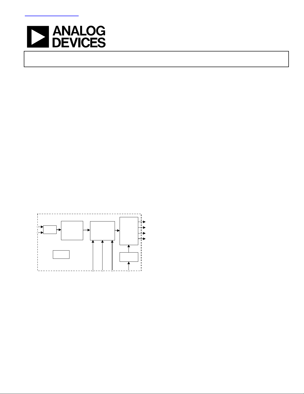
FUNCTIONAL BLOCK DIAGRAM
Thermistor
Inpu
Temp
Set Input
Error
Amplifier
Reference
Compensation
Network
2.5V
PID
Heating
ILim
Limiter
Controls
Cooling
ILim
VLim
MOSFET
Drivers
Oscillator
Freq/Phase
Control
Voltage outputs are provided to monitor both the temperature
of the object and the voltage across the TEC. A 2.5V voltage
reference is provided for the thermistor temperature sensing
bridge.
An external sense resistor provides true current sensing.
Current limits for both heating and cooling can be set
independently.
Rev. PrC
Information furnished by Analog Devices is believed to be accurate and reliable.
However, no responsibility is assumed by Analog Devices for its use, nor for any
infringements of patents or other rights of third parties that may result from its use.
Specifications subject to change without notice. No license is granted by implication
or otherwise under any patent or patent rights of Analog Devices. Trademarks and
registered trademarks are the property of their respective companies.
One Technology Way, P.O. Box 9106, Norwood, MA 02062-9106, U.S.A.
Tel: 781.329.4700 www.analog.com
Fax: 781.326.8703 © 2004 Analog Devices, Inc. All rights reserved.

ADN8831 PRELIMINARY TECHNICAL DATA
TABLE OF CONTENTS
Specifications 3
Theory of Operation 9
Absolute Maximum Ratings 5
Pin Configuration......................................................................... 6
Pin Descriptions ........................................................................... 6
REVISION HISTORY
Revision PrC
7/03—Data Sheet Changed from REV PrB to REV PrC.
Introduction...................................................................................9
Outline Dimensions 10
Ordering Guide 11
Rev. C | Page 2 of 11

PRELIMINARY TECHNICAL DATA ADN8831
SPECIFICATIONS
Table 1. ADN8831—Electrical Characteristics (V+ = 3.0 V to 5.5 V, TA = 25°C, unless otherwise noted.)
Parameter Symbol Conditions Min Typ Max Unit
TEMPERATURE STABILITY
Long Term Stability 10 kΩ thermistor with α = -4.4% at 25C 0.01 °C
PWM OUTPUT DRIVERS
Output Transition Time tR, tF C
Nonoverlapping Clock Delay 50 65 ns
Output Resistance R
Output Voltage Swing SFB V
Output Voltage Ripple ∆SFB f
Output Current Ripple ∆I
LINEAR OUTPUT AMPLIFIER
Output Resistance
Output Voltage Swing LFB 0 VDD V
POWER SUPPLY
Power Supply Voltage
Supply Current
Shutdown Current
Soft-Start Charging Current
Undervoltage Lockout UVLO Low to high threshold 2.5 2.7 V
Standby Current
Standby Threshold
ERROR AMPLIFIERS
Input Offset Voltage
Input Voltage Range V
Common-Mode Rejection Ratio CMRR
Output Voltage Range V
Power Supply Rejection Ratio PSRR
Output Current I
Gain Bandwidth Product GBW
OSCILLATOR
Sync Range f
Oscillator Frequency f
Free-Run Oscillation Frequency f
Phase Adjustment Range
Phase Adjustment Default
REFERENCE VOLTAGE
Reference voltage V
LOGIC OUTPUTS
Logic Low Output Level TEMPGD, SYNCOUT 0.2 V
Logic High Outut Threshold
= 3,300 pF 20 ns
L
O(N1,P1)
f
TEC
IL = 10 mA
= 0 V 0 VDD V
LIM
= 1 MHz 0.2 %
CLK
= 1 MHz 0.2 %
CLK
6 Ω
R
O, LNGATE
R
O, LPGATE
I
OUT
I
OUT
= 2 mA
= 2 mA
85
178
Ω
Ω
V
DD
PWM not switching
I
SY
I
SD
I
SS
I
SB
V
SB
3.0 5.5 V
-40C ≤ TA ≤ +85
SYNCIN/
SD
= 0 V
8
5 µA
12
15
mA
mA
2 µA
SINCIN/
SYNCIN/
SD
= VDD, SS/SB = 0 V
SD
= VDD
1 mA
200 300 mV
V
OS1
V
OS2
0
CM1,2
120 dB
1,2
0
OUT1,2
1,2
-5 +5 mA
OUT1,2
2 MHz
1,2
= 1.5 V, V
V
CM1
V
= 1.5 V, V
CM2
3.0 V ≤ V
DD
IN1P
IN2P
≤ 5.0 V
– V
– V
IN1M
IN2M
10
10
100
100
V
DD
V
DD
µV
µV
V
V
120 dB
CLK
CLK
CLK
SYNCIN/SD connected to external clock
SD
DD
= VDD
DD
, RFREQ = 150kΏ,
,
COMPOSC = V
SYNCIN/
COMPOSC = V
200 1,000 KHz
800 1,000 1,250 kHz
100 1000 KHz
SYNCIN/SD = VDD
Φ
CLK
Φ
CLK
0.1 V ≤ V
PHASE = open 180 °
≤ 2.4 V 25 335 °
PHASE
I
REF
< 2mA 2.37 2.47 2.57 V
REF
V
-
V
DD
0.2V
Rev. C | Page 3 of 11

ADN8831 PRELIMINARY TECHNICAL DATA
Table 2. ADN8831—Electrical Characteristics (V+ = 3.0 V to 5.5 V, TA = 25°C, unless otherwise noted.)
Parameter Symbol Conditions Min Typ Max Unit
TEC CURRENT MEASUREMENT
ITEC Gain A
ITEC Output Range V
ITEC Input Range V
ITEC Bias Voltage V
ITEC Output Current I
TEC VOLTAGE MEASUREMENT
VTEC Gain A
VTEC Output Range V
VTEC Bias Voltage V
VTEC Output Current I
VOLTAGE LIMIT
VLIM Gain A
VLIM Input Range V
VLIM Input Current, cooling I
VLIM Input Current, heating I
VLIM Input Current Accuracy,
heating
CURRENT LIMIT
ILIMC Input Voltage Range V
ILIMH Input Voltage Range V
ILIMC Limit Threshold V
ILIMH Limit Threshold V
TEMPERATURE GOOD
High Threshold V
Low Threshold V
V
V,ITEC
0 VDD V
ITEC
0 VDD V
CS, VLFB
V
ITEC, B
1 mA
OUT,TEC
/(V
ITEC
= VCS = 0 1.2 1.25 1.3 V
LFB
) 98 100 102 V/V
LFB-VCS
V
V,VTEC
0 2.5 V
VTEC
V
VTEC,B
1 mA
VTEC
VTEC
LFB
/(V
= V
) 0.23 0.25 0.27 V/V
LFB-VSFB
= 2.5V 1.2 1.25 1.3 V
SFB
V
V,LIM
0 VDD V
VLIM
V
VLIM,COOL
V
VLIM,HEAT
I
I
VLIM,HEAT
VLIM/IFREQ
5 V/V
SFB/VVLIM
< 1.25V 100 nA
OUT2
>1.25V I
OUT2
mA
FREQ
0.9 1.0 1.1 A/A
1.25 VDD V
ILIMC
0 1.25 V
ILIMH
V
TH,ILIMC
V
TH,ILIMH
= 2.0V 1.98 2.0 2.02 V
ITEC
= 0.5V 0.48 0.5 0.52 V
ITEC
IN2M tied to OUT2, V
OUT1,TH1
IN2M tied to OUT2, V
OUT1,TH2
= 1.5V 1.525 1.530 V
IN2P
= 1.5V 1.470 1.475 V
IN2P
Rev.Pr C | Page 4 of 11

PRELIMINARY TECHNICAL DATA ADN8831
ABSOLUTE MAXIMUM RATINGS
Table 3. Absolute Maximum Ratings (at 25°C, unless
otherwise noted)
Parameter Rating
Supply Voltage 6 V
Input Voltage GND to Vs + 0.3V
Storage Temperature Range –65°C to +150°C
Operating Temperature Range –40°C to +85°C
Operating Junction Temperature 125°C
Lead Temperature Range (Soldering, 60 Sec) 300°C
Table 2. Thermal Resistance
Package Type
32-lead LFCSP (ACP) 35 10 °C/W
1
θJC
θ
JA
Unit
1
θJA is specified for the worst-case conditions, i.e., θJA is specified for device
soldered in circuit board for surface mount packages.
Rev. C | Page 5 of 11

ADN8831 PRELIMINARY TECHNICAL DATA
Pin Configuration
Pin Descriptions
Pin No. Mneumonic Type Description
1 ILIMC Analog Input Analog input sets TEC cooling current protection limit.
2 IN1P Analog Input Non-inverting input to error amplifier.
3 IN1M Analog Input Inverting input to error amplifier.
4 OUT1 Analog Output Output of error amplifer.
5 IN2P Analog Input Non-inverting input to compensation amplifier.
6 IN2M Analog Input Inverting input to compensation amplifier.
7 OUT2 Analog Output Output of compensation amplifier.
8 VREF Analog Output 2.5V Voltage Reference output.
9 AVDD Power Power for non-driver sections. 3.0 V min; 5.5V max.
10 PHASE Analog Input Sets SYNCOUT clock phase relative to SYNCIN clock.
11 TMPGD Digital Output
12 AGND Ground Analog ground. Connect to low noise ground.
13 FREQ Analog Input Sets switching frequency with an external resistor.
14
15 SYNCO Digital Output
16
17 COMPOSC Analog Output Comensation for oscillator; connect capacitor to ground.
18 PVDD Power Power for output driver sections. 3.0V min; 5.5V max.
19 SPGATE Analog Output Drives PWM output external PMOS gate.
20 SWITCH Analog Input Connects to PWM FET drains.
21 SNGATE Analog Output Drives PWM output external NMOS gate.
22 PGND Ground Power ground. External NMOS devices connect to PGND. Connect to digital ground.
23 SFB Analog Input PWM feedback. Typically connects to TEC- pin of TEC.
24 COMPSW Analog Input Comensation for switching amplifier.
25 LPGATE Analog Ouput Drives linear output external PMOS gate.
26 LNGATE Analog Output Drives linear output external NMOS gate.
27 LFB Analog Input Linear feedback. Will typically connect to TEC+ pin of TEC.
28 CS Analog Input Connect to output current sense resistor.
29 ITEC Analog Ouput Indicates TEC current.
30 VTEC Analog Ouput Indicates TEC voltage.
31 VLIM Analog Input Sets maximum TEC voltage.
32 ILIMH Analog Input Sets TEC heating current protection limit.
SS/SB
SYNCI/SD
Analog Input
Digital Input
Indicates when thermistor temperature is within ±0.01°C if target temperature as
set by TEMPSET voltage.
Sets soft-start time for output voltage. Pull low to put ADN8831 into standby mode
(VTEC = 0V).
Phase adjustment clock output. Phase set from PHASE pin. Used to drive SYNCIN of
other ADN8831 devices.
Optional clock input. If not connected, clock frequency is set by FREQ pin. Pull low
to put ADN8831 into shutdown mode.
Rev.Pr C | Page 6 of 11

PRELIMINARY TECHNICAL DATA ADN8831
DETAILED BLOCK DIAGRAM
Figure 2. Detailed Block Diagram
Rev. C | Page 7 of 11

ADN8831 PRELIMINARY TECHNICAL DATA
TYPICAL APPLICATION CIRCUIT
Figure 3. Typical Application Circuit I
Rev.Pr C | Page 8 of 11

PRELIMINARY TECHNICAL DATA ADN8831
THEORY OF OPERATION
Introduction
The ADN831 is a thermoelectric cooler (TEC) controller used
to set and stabilize the temperature of the TEC. A voltage
applied to the input of the ADN8831 corresponds to a target
temperature set-point. Using a thermistor to monitor the
current temperature of the target object, the ADN8831 applies
the appropriate current to the TEC to pump heat either towards
or away from the target object until the set-point temperature is
reached.
Self correcting auto-zero amplifiers (chop1 and chop2) are used
in the input and compesation stages of the aDN8831 to provide
a maximum offset voltage of 100uV over time and temperature.
This results in a final temperature accuracy of 0.01C in typical
applications, eliminating the ADN8831 as an error source in the
temperature control loop.
The TEC is driven differentially using an H-bridge
configuration. The ADN8831 drives external transistors that are
used to provide the current to the TEC. The maximum voltage
across the TEC and current flowing through the TEC can be set
using the VLIM and ILIM pins. Additional details are provided
in the Setting Voltage and Current Limits section.
One side of the H-bridge uses a switched output, while the
other is linear. This proprietary configuration allows the
ADN8831 to provide efficiency of >90%, while minimizing
external filtering component count. The ADN8831 requires
only one inductor and one capacitor to filter the switching
frequency of the switched output. For most applications, a
4.7uH inductor, a 22uF capacitor and a switching frequency of
1MHz maintains less than 0.5% worst-case output voltage ripple
across the TEC.
The switched output is controlled by the ADN8831’s oscillator.
A single resistor on the FREQ pin (pin #13) sets the switching
frequency from 100kHz to 1MHz. The clock output is available
at the SYNCO pin (pin #15). Connecting SYNCO to the SYNI
pin of another ADN8831 allows multiple ADN8831s to be
driven using a single clock.
The clock phase can be changed using a simple resistor divider
at the PHASE pin )pin #10). Phase adjustment allows two or
more ADN8831 devices to operate from the same clock
frequency and not have all outputs switch simultaneously,
which could create excessive power supply ripple. Details of
how to adjust the clock frequency and phase are provided in the
Setting the Frequency section.
The logic output of the TEMPGD pin (pin #11) indicates when
the target temperature is reached. Shutdown, standby, and true
current-sensing are also provided by the ADN8831 to protect
from catastrophic system failures that could damage the TEC.
Rev. C | Page 9 of 11

ADN8831 PRELIMINARY TECHNICAL DATA
OUTLINE DIMENSIONS
Figure 1. 32-Lead Lead Frame Chip Scale Package [LFCSP]
(CP-32)
Dimensions Shown in Millimeters
ESD CAUTION
ESD (electrostatic discharge) sensitive device. Electrostatic charges as high as 4000 V readily accumulate on the
human body and test equipment and can discharge without detection. Although these products feature
proprietary ESD protection circuitry, permanent damage may occur on devices subjected to high energy
electrostatic discharges. Therefore, proper ESD precautions are recommended to avoid performance
degradation or loss of functionality.
Rev.Pr C | Page 10 of 11

PRELIMINARY TECHNICAL DATA ADN8831
ORDERING GUIDE
Table 3.
Model Temperature Range Package Description Package Option
ADN8831ACP
ADN8831-EVAL
-40°C to +85°C
-40°C to +85°C
32-Lead Lead Frame Chip Scale Package CP-32
Evaluation Board
© 2003 Analog Devices, Inc. All rights reserved. Trademarks and
registered trademarks are the property of their respective companies.
PR04663-0-2/04(PrC)
Rev. C | Page 11 of 11
 Loading...