

EDFA and CW Laser Controller
Preliminary Technical Data
FEATURES
Four Operational Modes Including:
Constant Laser Current
Constant Optical Output Power
Constant EDFA Gain
Constant Laser Power
High Power Efficiency: >90%
Three Built-In Photodiode TIAs
Adjustable Laser Diode and EDFA Protection Limits
Free-run or Synchronous Switching Frequency Modes
Adjustable Phase Delay for Synchornous Clock Mode
Optional Dithering Built-In
Programmable Dither Frequency and Amplitude
APPLICATIONS
EDFA Pump Laser Diode Control
CW Laser Bias Control
Raman Amplifiers
GENERAL DESCRIPTION
The ADN8820 is a versatile Continuous Wave (CW) and EDFA
laser diode driver and controller. It provides a low noise and
precise current control for driving a source or pump laser diode.
ADN8820
Output Power (COP), or Constant EDFA Gain (CG). Multiple
pump laser applications are easily supported by the ADN8820.
Common-cathode-to-ground and common-anode-to-VDD
configurations are also supported.
The ADN8820 has a high speed closed-loop control, making it
suitable for add/drop applications in telecommunication
systems. It has a low-current shutdown mode and a soft-start
feature to minimize power supply bounce on start-up.
Protection circuitry is built into the device. The protection
limits are easily adjustable and are used to set maximum output
current and voltage, optical output power, EDFA gain, and
pump or CW laser power.
The output stage consists of a high-efficiency PWM amplifier in
parallel with a high-speed linear amplifier. This provides the
fastest settling time response along with the lowest power and
heat dissipation. A pair of external MOSFETs on the PWM
amplifier provide output currents of up to 5A.
Three low-bias current TIAs are built-in. These allow
amplification for the laser back-facet photodiode and EDFA
input and output photodiodes. For CW laser applications, the
two unused TIAs can be used for etalon photodiode
amplification, allowing continuous wavelength monitoring.
*
It can be set to operate in one of four controller modes:
Constant Current (CC), Constant Laser Power (CLP), Constant
FUNCTIONAL BLOCK DIAGRAM
*
U.S. Patent Pending
Rev. PrB
Information furnished by Analog Devices is believed to be accurate and reliable.
However, no responsibility is assumed by Analog Devices for its use, nor for any
infringements of patents or other rights of third parties that may result from its use.
Specifications subject to change without notice. No license is granted by implication
or otherwise under any patent or patent rights of Anal og Devices.
The ADN8820 is available in a 7 x 7 mm lead-frame chip scale
package (LFCSP) with a package height of less than 1 mm.
One Technology Way, P.O. Box 9106, Norwood, MA 02062-9106, U.S.A.
Tel: 781/329-4700 www.analog.com
Fax: 781/326-8703 © 2003 Analog Devices, Inc. All rights reserved.

ADN8820 - SPECIFICATIONS1 Preliminary Technical Data
Table 1. ADN8820—Electrical Characteristics (AVDD = PVDD = 5V, AGND = PGND = 0V, TA = 25°C, using typical
circuit in Figure 1, unless otherwise noted.)
2
Parameter Symbol Conditions Min Typ Max Unit
TRANSIMPEDANCE AMPLIFIERS
Detection Range IIP From IPDIN Photodiode
I
I
Input Bias Current IB
IB
IB
From OPDIN Photodiode 0.005 5,000
OP
LP
IPDIN
OPDIN
LPDIN
From LPDIN Photodiode 5 5,000
IPDIN, OPDIN, LPDIN Amplifier 100 pA
Inputs 100 pA
100 pA
0.005 5,000
µA
µA
µA
Input Voltage Range VBLP, VB 0 VDD V
Monitor Output Range V
V
V
Input Offset Voltage V
V
V
Maximum Output Current I
I
I
Gain-Bandwidth Product GBW
GBW
GBW
IPO
LPO
OPO
OSIP
OSOP
OSLP
OUTIPO
OUTLPO
OUTOPO
IP
OP
LP
IPO, LPO, OPO Outputs 0 VDD V
0 VDD V
0 VDD V
IPDIN, OPDIN, LPDIN Amplifiers 10
10
µV
µV
2 mV
IPO, LPO, OPO Outputs ±10 mA
±10 mA
±10 mA
IPDIN, OPDIN, LPDIN Amplifiers 10 MHz
10 MHz
1 MHz
LIMIT CONTROLS
Input Voltage Range V
INLIM
IPMIN, OPLIM, LPLIM, ILIM, and
0 2.6 V
VLIM
Limiter Accuracy V
Open Circuit Voltage V
OSLIM
LIMNC
OPLIM, LPLIM, ILIM, IPMIN ±10 mV
Voltage for OPLIM, LPLIM, and ILIM
2.5 2.6 2.7 V
with no connection
Pull-up Current IB
LIM
Flowing out of OPLIM, LPLIM, and
500 nA
ILIM with LIM Voltage <2.0V
IPMIN Disable Threshold V
VLIM Input Bias Current I
VLIM Voltage Control Accuracy |V
V
IPMINLO
VLIM
= 0V 200 mV
IPO
Flowing into VLIM pin 1
– VLIM| 50 mV
LINOUT
µA
ERROR AMPLIFIER
Input Offset Voltage V
Input Common-Mode Voltage Range V
Output Voltage Swing V
Maximum Output Current I
OSEA
CMEA
OUTEA
MAXEA
Gain-Bandwidth GBW
EA
10 25
µV
0 VDD V
0 VDD V
±10 mA
10 MHz
SET INPUT
Input Voltage Range V
Input Bias Current IB
SET
SET
0 VDD V
±1
µA
MULTIPLEXERS
Ouput Impedance 100
Ω
Output Voltage Range 0 VDD V
1
Specifications subject to change without notice
2
Capital letters denote pin names.
Rev. PrB | Page 2 of 9

ADN8820 - SPECIFICATIONS1 Preliminary Technical Data
Table 1. ADN8820—Electrical Characteristics (AVDD = PVDD = 5V, AGND = PGND = 0V, TA = 25°C, using typical
circuit in Figure 1, unless otherwise noted.)
2
Parameter Symbol Conditions Min Typ Max Unit
LINEAR OUTPUT
Short-Circuit Output Current I
Output Voltage Compliance V
V
Power Supply Rejection Ratio PSRR
Gain-Bandwidth Product GBW
OUTLIN
LINMAX
LINMIN
LIN
LIN
300 mA
I
= 300mA (sourcing) 4.5 V
OUTLIN
I
= -160mA (sinking) 0.5 V
OUTLIN
68 dB
10 MHz
PWM OUTPUT
Offset Voltage V
V
OSPWM
= LINOUT - FB ±10 mV
OSPWM
Non-Overlap Delay
Output Transistion Time tR, tF
Output Driver Resistance R
R
NGATE
PGATE
Output Current Ripple I
Soft-Start Time
Standby Mode Threshold V
SSSB
≤ 3nF
FET C
ISS
6
6
= 300mA, V
OUT
= 0.1 µF
C
SS
= 2V 1 %
OUT
PWM and LINOUT disabled 0.4 V
40 ns
Ω
Ω
15 ms
OSCILLATOR
Free-Run Oscillation Frequency f
CLK
CMPOSC = VDD; SYNCIN = 0V 100 1,000 kHz
Synchornization Capture Range SYNCIN driven with external clock 100 1,000 kHz
Phase Adjustment
φ
CLK
45 315 degrees
CURRENT SENSE AMPLIFIER
Input Common-Mode Voltage Range V
Input Resistance R
Output Offset Voltage V
Gain A
Output Voltage Range V
CMCS
INCS
OSLIO
VCS
LIO
0 VDD V
10.5
V
= V
CSP
V
LIO
= 2.5V 1 mV
CSN
/ (V
– V
CSP
) 20 V/V
CSN
kΩ
0 VDD V
DITHER GENERATOR
Frequency Range f
Frequency Multiplier Programming
DITHER
xx kΩ ≤ RT ≤ xx kΩ
See Table II
0.2 2 MHz
Voltage
Dither Current Control Votlage V
Programming Current Range I
Maximum DO Output Current I
DO Output Voltage V
V
DCTL
V
DCTL
MAXDO
DO
LIO
LIO
±19 ±20 ±21 mA
1.5 V
= 2.5 V 1.2 1.25 1.3 V
= 2.5 V 0 100
µA
POWER SUPPLY
Power Supply Range VDD 3.0 5.5 V
Supply Current ISY
Shutdown Current I
Standby Current I
Undervoltage Lockout V
SD
SB
UVLO
SD
DSEL/
-40°C ≤ T
≥ 0.8V; I
≤ +85°C
A
OUT
= 0A
DSEL/SD ≤ 0.2V
SS/SB ≤ 0.2V
2.4 2.5 V
25 30 mA
10
µA
2.5 mA
REFERNCE OUTPUT
Reference Voltage V
REF
Power Supply Rejection Ratio PSRR
REF
I
≤ 2 mA
REF
With respct to AVDD 68 V
2.4 2.5 2.6 V
1
Specifications subject to change without notice
2
Capital letters denote pin names.
Rev. PrB | Page 3 of 9

ADN8820 - SPECIFICATIONS1 Preliminary Technical Data
Table 1. ADN8820—Electrical Characteristics (AVDD = PVDD = 5V, AGND = PGND = 0V, TA = 25°C, using typical
circuit in Figure 1, unless otherwise noted.)
2
Parameter Symbol Conditions Min Typ Max Unit
DUAL OUTPUT
Output Voltage Range V
Voltage Gain A
CONTROL LOOP STATUS OUTPUT
CLGD High V
CLGD Low V
LOGIC CONTROL
Logic Low Input Threshold V
Logic High Input Threshold V
Logic Low Output Level V
Logic High Output Level V
DUAL
VDUAL
CLGDHI
CLGDLO
IL
IH
OL
OH
≤ 500 µA
I
DUAL
A
= DUAL / LIO; V
VDUAL
with 1.9 V ≤ V
≤ 2.1V
LIO
= 2.25V
ILIM
0.05 x VDD ≤ V
≤ 0.95 x VDD
EAOUT
Otherwise 0.2 V
MODE0, MODE1, SYNCIN 0.2 V
MODE0, MODE1, SYNCIN VDD-0.2 V
0.2 V
VDD-0.2 V
Input Current ±1
0.4 VDD-0.4 V
20 V/V
4.8 V
µA
1
Specifications subject to change without notice
2
Capital letters denote pin names.
Figure 1. Typical Application Circuit
Rev. PrB | Page 4 of 9

ADN8820 Preliminary Technical Data
ABSOLUTE MAXIMUM RATINGS
Table 2. Absolute Maximum Ratings (at 25°C, unless
otherwise noted)
Parameter Rating
Supply Voltage 6 V
Output Short-Circuit Duration to GND Indefinite
Storage Temperature Range –65°C to +150°C
Operating Temperature Range –40°C to +85°C
Junction Temperature Range: CP Packages –65°C to +150°C
Lead Temperature Range (Soldering, 60 Sec) 300°C
Table 3. Thermal Resistance
Package Type
LFSCP-48 (CP-48) 32 12 °C/W
1
θJA is specified for the worst-case conditions, i.e., θJA is specified for device
soldered in circuit board for surface mount packages.
1
θJC
θ
JA
Unit
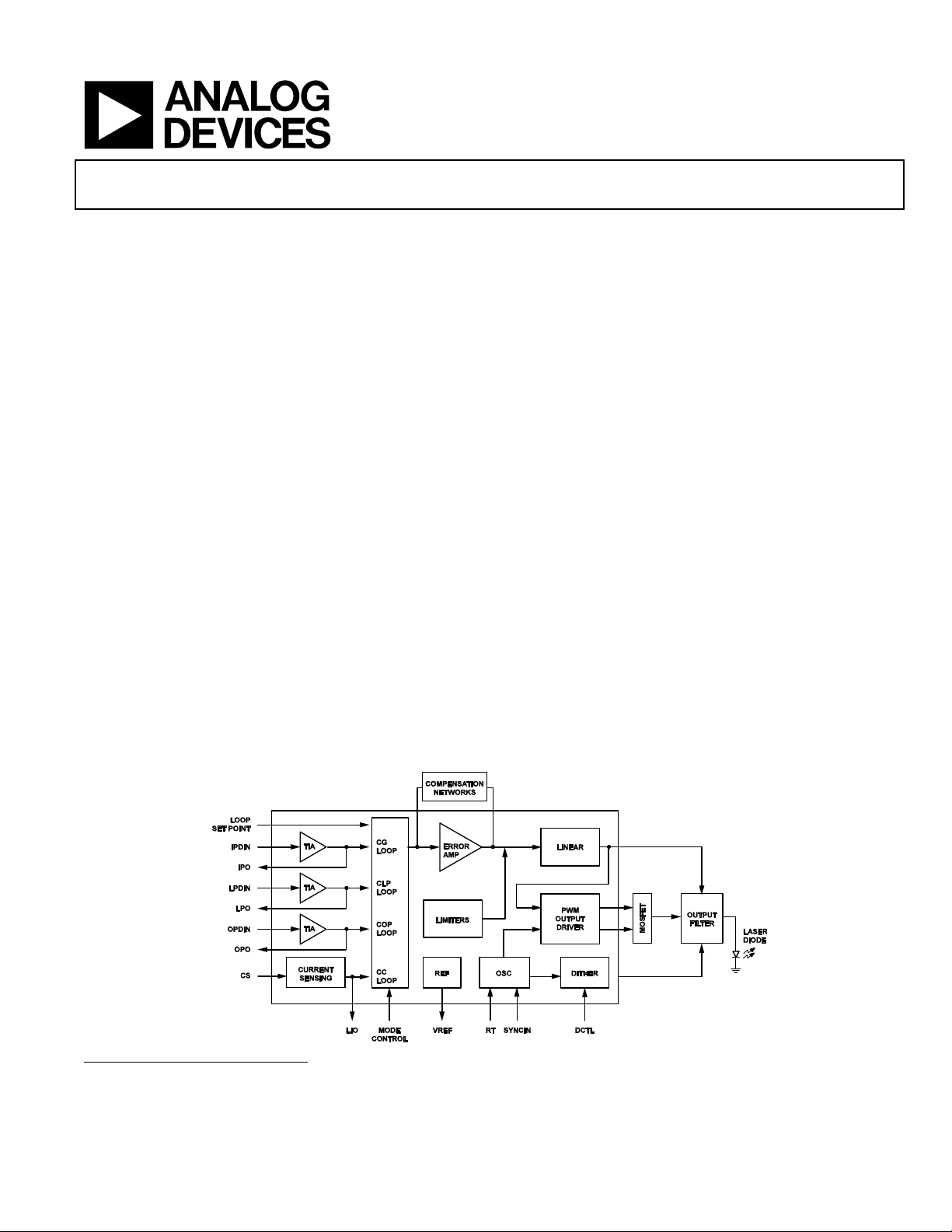
Figure 2. System Block Diagram
PIN CONFIGURATION
Rev. PrB | Page 5 of 9

ADN8820 Preliminary Technical Data
PIN FUNCTIONS
Name Pin Function Connections
AMPLIFIER INPUTS
IPDIN 3 Input to TIA for EDFA input photodiode EDFA input photodiode and feedback resistor
LPDIN 6 Input to TIA for laser photodiode Laser photodiode and feedback resistor
OPDIN 9 Input to TIA for EDFA output photodiode EDFA output photodiode and feedback resistor
VB 2 Bias voltage for EDFA input and output photodiodes External bias voltage required
VBLP 5 Bias voltage for laser photodiode External bias voltage required
CSP 37 Non-inverting input of current sense amplifier
CSN 38 Inverting input of current sense amplifier
LIMIT INPUTS
VLIM 1 Laser diode voltage will not exceed VLIM External voltage required
ILIM 45 Limits output voltage if LIO > ILIM External voltage or no connection (defaults to 2.5 V)
OPLIM 47 Limits output voltage if OPO > OPLIM External voltage or no connection (defaults to 2.5 V)
LPLIM 46 Limits output voltage if LPO > LPLIM External voltage or no connection (defaults to 2.5 V)
IPMIN 48 Limits output voltage if IPO is lower than IPMIN External voltage required
ERROR (COMPENSATION) AMPLIFIER (EA)
EANLP 41 Compensation network for laser diode loop
EANOP 40 Compensation network for EDFA loop
EAOUT 39 Output of compensation amplifier Internal connection to linear output amplifier
MUX 42
OPCMP 44 Compensation for limiter section R-C network to ground
SET 8
POWER OUTPUT AMPLIFIERS
LINOUT 33 Linear amplifier output
PGATE 30 PWM switching for PMOS Gate of external PMOS for PWM output
NGATE 31 PWM switching for NMOS Gate of external NMOS for PWM output
SWITCH 28 PWM amplifier output Drains of external NMOS, PMOS, and input of L-C filter
FB 24 Feedback input for PWM amplifier Output of L-C filter and laser diode
PWMCMP1 23 Compensation for PWM amplifier Series R-C networks to FB and PWMCMP2
PWMCMP2 22 Compensation for PWM amplifier Series R-C to PWMCMP1
SB
SS/
OUTPUT MONITOR VOLTAGES
IPO 4 Output of EDFA input photodiode TIA Feedback resistor to IPDIN
OPO 10 Output of EDFA output photodiode TIA Feedback resistor to OPDIN
LPO 7 Output of laser diode photodiode TIA Feedback resistor to LPDIN
LIO 11 Output of current sense amplifier
DUAL 12 Compares LIO to 90% of ILIM
EAOUT 39 Output of compesnation amplifier Internal connection to linear output amplifier
OSCILLATOR SECTION
SYNCIN 27 Optional clock input signal for PLL Ground or external clock
SYNCOUT 26 Follows rising edge of SYNCIN plus phase shift
CMPOSC 16 Compensation for synchronizing PLL R-C network to ground
PHASE 17 Sets rising edge phase shift of SYNCOUT External voltage or no connection (default is 0.7V)
RT 15 Sets PWM clock frequency Resistor (RT) to ground
25
Allows separate compensation for EDFA and laser
diode
Sets output power or current based on MODE
settings
Constant current charges external capacitor to softstart PWM output from 0% duty cycle
High-side of laser current sense resistor (50 mΩ typ.)
Low-side of laser current sense resistor (50 mΩ typ.)
Internally connects inverting input of EA to laser diode
compensation network
Internally connects inverting input of EA to EDFA
compensation network
Connects to two external compensation networks: one
for EDFA loop, one for laser diode loop
External voltage or DAC
Laser diode through 1 Ω series resistor
Optional external FET can pull down and to engage
standby mode
To SET pin of additional ADN8820 device in multipump optical amplifier applications
Optional connection to SYNCIN of additional ADN8820
device
Rev. PrB | Page 6 of 9

ADN8820 Preliminary Technical Data
Name Pin Function Connections
DITHER GENERATOR
DSEL/SD
21
4-level logic input to set dither frequency or engage
shutdown
DCTL 36
Sets dither current as a percentage of the laser
diode current
DO 35 Optional dither AC current to laser diode To laser diode through 1 nF series capacitor
LOGIC INPUTS
MODE1 18 Sets control loop mode (see Table I) External logic voltage
MODE0 19 Sets control loop mode (see Table I) External logic voltage
DSEL/
SB
SS/
SD
21 Pulling voltage low engages shutdown External voltage
25 Pulling voltage low engages standby
LOGIC OUTPUTS
CLGD 20
Logic high if EAOUT is within 5% to 95% of AVDD;
Logic low otherwise
POWER
PVDD 29, 34 Power for output amplifiers and digital sections 3.0 V to 5.5 V
AVDD 43 Low noise power for TIAs, limiter section, and EA 3.0 V to 5.5 V
PGND 32 Current return for output amplifiers 0 V
AGND 14 Low noise ground 0 V
VREF 13 2.5 V reference voltage
External voltage
Resistor (R
) to ground
DCTL
470 pF soft-start capacitor to ground; optional external
FET can pull down to engage standby
Can be used as refernce for VB, VBLP, SET, and limiter
inputs
TABLE 4. MODE CONTROL LOGIC
MODE Inputs Error Amplifier MUX
MODE1 MODE0 Mode Setting -Input +Input Output Description
0 0 Constant Current EANLP SET LIO
Maintains a fixed current through laser diode;
generally used for calibration.
0 1 Constant Laser Power EANLP SET LPO
Maintains a constant optical output power from
laser diode.
1 0 Constant Ouptut Power EANOP SET OPO
Maintains a constant optical power at output of
EDFA.
1 1 Constant Gain EANOP IPO OPO
Monitors both input and output optical power
to maintain constant gain from optical amplifier.
TABLE 5. PWM CLOCK FREQUENCY SELECTION LEVELS
PWM Clock Frequency
÷2
f
DITHER
÷4
f
DITHER
÷8
f
DITHER
Note: f
DSEL/SD (V)
Min Max Mode Division
0 0.5 Shutdown N/A
0.7 1.2 Active
1.3 1.8 Active
2.0 VDD Active
is the ADN8820 dither frequency and is set by a resistor connected from RT to ground.
DITHER
Rev. PrB | Page 7 of 9

ADN8820 Preliminary Technical Data
OUTLINE DIMENSIONS
Figure 3. 48-Lead Frame (LFCSP-48) Chip Scale Package
7 x 7 mm Body
(CP-48)
Dimensions Shown in Millimeters
ESD CAUTION
ESD (electrostatic discharge) sensitive device. Electrostatic charges as high as 4000 V readily accumulate on the
human body and test equipment and can discharge without detection. Although these products feature
proprietary ESD protection circuitry, permanent damage may occur on devices subjected to high energy
electrostatic discharges. Therefore, proper ESD precautions are recommended to avoid performance
degradation or loss of functionality.
Rev. PrB | Page 8 of 9

ADN8820 Preliminary Technical Data
ORDERING GUIDE
Table 6. ADN8820 Ordering Guide
Product
ADN8820 48-Lead LFCSP CP-48 TBD N/A –40 to +125
ADN8820-REEL7 48-Lead LFCSP CP-48 TBD TBD –40 to +125
ADN8820-EVAL Eval board N/A N/A N/A –40 to +125
Package
Description
Package
Option
Top
Mark
No. of Parts
per Reel
Temperature
Range (°C)
© 2003 Analog Devices, Inc. All rights reserved. Trademarks and
registered trademarks are the property of their respective companies.
C02747-0-4/03(C)
Rev. PrB | Page 9 of 9
 Loading...