

3.75 Gbps Quad Bidirectional
q
FEATURES
Optimized for dc to 3.75 Gbps data
Programmable input equalization
Up to 22 dB boost at 1.875 GHz
Compensates up to 30 meters of CX4 cable up to 3.75 Gbps
Compensates up to 40 inches of FR4 up to 3.75 Gbps
Programmable output pre-emphasis/de-emphasis
Up to 12 dB boost at 1.875 GHz (3.75 Gbps)
Compensates up to 15 meters of CX4 cable up to 3.75 Gbps
Compensates up to 40 inches of FR4 up to 3.75 Gbps
Flexible 1.8 V to 3.3 V core supply
Per lane P/N pair inversion for routing ease
Low power: 125 mW/channel up to 3.75 Gbps
DC- or ac-coupled differential CML inputs
Programmable CML output levels
50 Ω on-chip termination
Loss-of-signal detection
Temperature range operation: −40°C to +85°C
Supports 8b10b, scrambled, or uncoded NRZ data
2
I
C control interface
64-lead LFCSP (QFN) package
APPLICATIONS
10GBase-CX4
HiGig™
InfiniBand®
1×, 2× Fibre Channel
XAUI™
Gigabit Ethernet over backplane or cable
CPRI™
50 Ω cables
CX4 E
ualizer
ADN8102
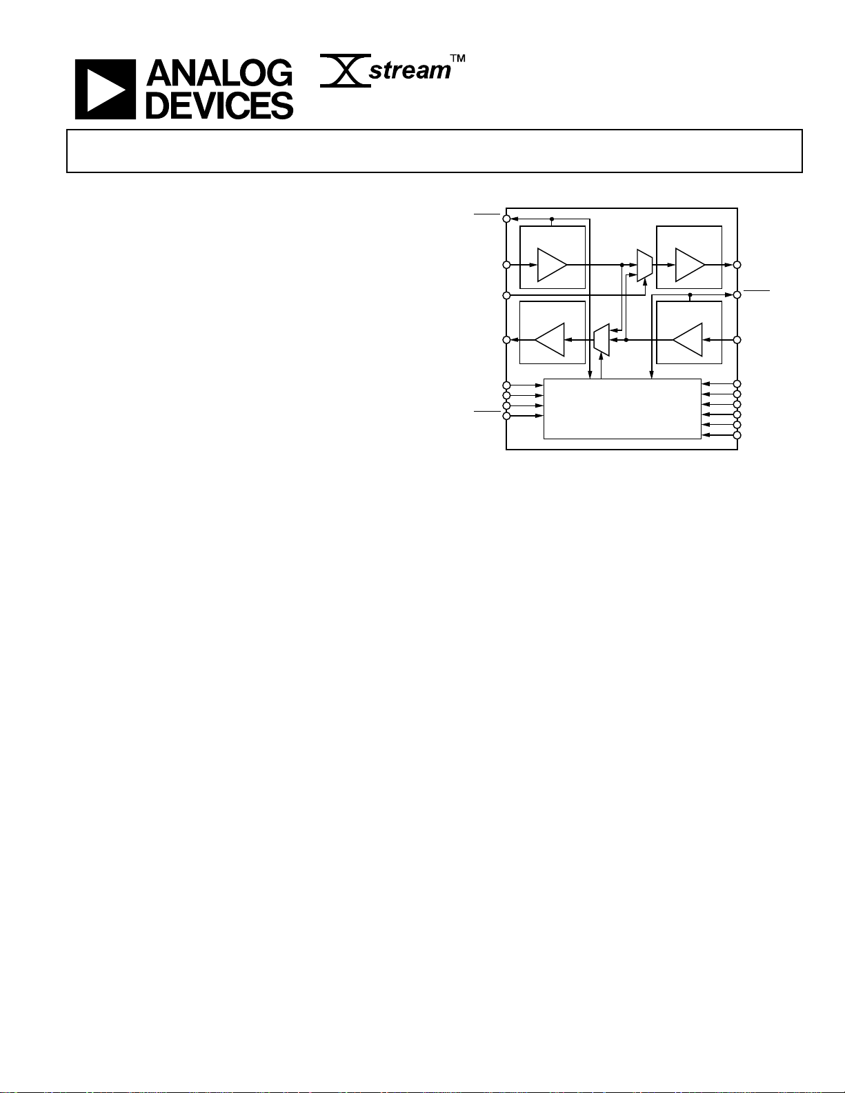
FUNCTIONAL BLOCK DIAGRAM
LOS_B
RECEIVE
EQUALIZ ATION
Ix_B[3:0]
Ox_A[3:0]
ADDR[1:0]
SCL
SDA
RESET
LB
EQ
TRANSMIT
PRE-EMPHASIS
PE
GENERAL DESCRIPTION
The ADN8102 is a quad, bidirectional, CX4 cable/backplane
equalizer with eight differential PECL-/CML-compatible inputs
with programmable equalization and eight differential CML
outputs with programmable output levels and pre-emphasis or
de-emphasis. The operation of this device is optimized for NRZ
data at rates up to 3.75 Gbps.
The receive inputs provide programmable equalization to
compensate for up to 30 meters of CX4 cable (24 AWG) or
40 inches of FR4, and programmable pre-emphasis to compensate
for up to 15 meters of CX4 cable (24 AWG) or 40 inches of FR4
at 3.75 Gbps. Each channel also provides programmable loss-ofsignal detection and loopback capability for system testing and
debugging.
The ADN8102 is controlled through toggle pins, an I
interface that provides more flexible control, or a combination of
both. Every channel implements an asynchronous path supporting
dc to 3.75 Gbps NRZ data, fully independent of other channels. The
ADN8102 has low latency and very low channel-to-channel skew.
The main application for the ADN8102 is to support switching
in chassis-to-chassis applications over CX4 or InfiniBand cables.
The ADN8102 is packaged in a 9 mm × 9 mm 64-lead LFCSP
(QFN) package and operates from −40°C to +85°C.
ADN8102
2:1
CONTROL LO GIC
Figure 1.
TRANSMIT
PRE-EMPHASIS
2:1
RECEIVE
EQUALIZ ATION
PE
EQ
Ox_B[3:0]
LOS_A
Ix_A[3:0]
EQ_A[1:0]
PE_A[1:0]
EQ_B[1:0]
PE_B[1:0]
ENA
ENB
2
C® control
07060-001
Rev. B
Information furnished by Analog Devices is believed to be accurate and reliable. However, no
responsibility is assumed by Analog Devices for its use, nor for any infringements of patents or other
rights of third parties that may result from its use. Specifications subject to change without notice. No
license is granted by implication or otherwise under any patent or patent rights of Analog Devices.
Trademarks and registered trademarks are the property of their respective owners.
One Technology Way, P.O. Box 9106, Norwood, MA 02062-9106, U.S.A.
Tel: 781.329.4700 www.analog.com
Fax: 781.461.3113 ©2008–2010 Analog Devices, Inc. All rights reserved.

ADN8102
TABLE OF CONTENTS
Features .............................................................................................. 1
Applications ....................................................................................... 1
Functional Block Diagram .............................................................. 1
General Description ......................................................................... 1
Revision History ............................................................................... 2
Specifications ..................................................................................... 3
Timing Specifications .................................................................. 5
Absolute Maximum Ratings ............................................................ 6
ESD Caution .................................................................................. 6
Pin Configuration and Function Descriptions ............................. 7
Typical Performance Characteristics ............................................. 9
Theory of Operation ...................................................................... 16
Introduction ................................................................................ 16
Receivers ...................................................................................... 17
Equalization Settings .................................................................. 17
Lane Inversion ............................................................................ 18
Loopback ..................................................................................... 20
Transmitters ................................................................................ 21
Selective Squelch and Disable ................................................... 24
I2C Control Interface ...................................................................... 25
Serial Interface General Functionality..................................... 25
I2C Interface Data Transfers—Data Write .............................. 25
I2C Interface Data Transfers—Data Read ............................... 26
Applications Information .............................................................. 27
Output Compliance ................................................................... 27
Printed Circuit Board (PCB) Layout Guidelines ................... 29
Register Map ................................................................................... 31
Outline Dimensions ....................................................................... 33
Ordering Guide .......................................................................... 33
REVISION HISTORY
10/10—Rev. A to Rev. B
Changes to Power Supply/Supply Current Parameter, Table 1 ... 4
Added t
Renumbered Sequentially ................................................................ 5
Added Junction Temperature Parameter, Table 3 ........................ 6
Changes to Introduction Section .................................................. 16
Added Table 5; Renumbered Sequentially .................................. 16
Changes to Equalization Settings Section ................................... 17
Added Table 7 and Advanced Equalization Settings Section ... 17
Changes to Table 8 .......................................................................... 18
Added Table 12 ............................................................................... 20
Changes to Loopback Section and Changes to Table 13 ........... 20
Added Table 14 ............................................................................... 21
Changes to Table 15 ........................................................................ 21
Changes to Table 17 ........................................................................ 22
Deleted High Current Setting and Output Level Shift
Section .............................................................................................. 23
Deleted Table 14; Renumbered Sequentially .............................. 24
Changes to Table 18 ........................................................................ 24
Added Table 19 ............................................................................... 24
Deleted Table 15 .............................................................................. 25
Added Applications Information Section and Output
Compliance Section ....................................................................... 27
Parameter and Note 1, Table 2 and Figure 3;
RESET
Moved TxHeadroom and Figure 44 ............................................. 27
Changes to TxHeadroom and Figure 44 ..................................... 27
Added Table 20 ............................................................................... 27
Added Table 21 ............................................................................... 28
Deleted Transmission Lines Section and Soldering Guidelines
for Chip Scale Package Section ..................................................... 28
Changes to Printed Circuit Board (PCB) Layout Guidelines
Section .............................................................................................. 29
Added Figure 45, Supply Sequencing Section, Thermal Paddle
Design Section, and Figure 46 ...................................................... 29
Added Stencil Design for the Thermal Paddle, Figure 47, and
Figure 48 .......................................................................................... 30
8/08—Rev. 0 to Rev. A
Changes to Features Section ............................................................ 1
Changes to Loss of Signal/Signal Detect Section ....................... 18
Added Recommended LOS Settings Section .............................. 18
Deleted Figure 39; Renumbered Sequentially ............................ 18
Exposed Paddle Notation Added to Outline Dimensions ........ 31
5/08—Revision 0: Initial Version
Rev. B | Page 2 of 36

ADN8102
SPECIFICATIONS
VCC = 1.8 V, VEE = 0 V, V
T
= 25°C, unless otherwise noted.
A
Table 1.
Parameter Test Conditions/Comments Min Typ Max Unit
DYNAMIC PERFORMANCE
Maximum Data Rate/Channel (NRZ) 3.75 Gbps
Deterministic Jitter Data rate < 3.75 Gbps; BER = 1 × 10
Random Jitter VCC = 1.8 V 1.5 ps rms
Residual Deterministic Jitter
With Input Equalization Data rate < 3.25 Gbps; 0 inches to 40 inches FR4 0.20 UI
Data rate < 3.25 Gbps; 0 meters to 30 meters CX4 0.19 UI
Data rate < 3.75 Gbps; 0 inches to 40 inches FR4 0.24 UI
Data rate < 3.75 Gbps; 0 meters to 30 meters CX4 0.21 UI
With Output Pre-Emphasis Data rate < 3.25 Gbps; 0 inches to 40 inches FR4 0.13 UI
Data rate < 3.25 Gbps; 0 meters to 15 meters CX4 0.37 UI
Data rate < 3.75 Gbps; 0 inches to 40 inches FR4 0.14 UI
Data rate < 3.75 Gbps; 0 meters to 15 meters CX4 0.41 UI
Output Rise/Fall Time 20% to 80% 75 ps
Propagation Delay 1 ns
Channel-to-Channel Skew 50 ps
OUTPUT PRE-EMPHASIS
Equalization Method 1-tap programmable pre-emphasis
Maximum Boost 800 mV p-p output swing 6 dB
200 mV p-p output swing 12 dB
Pre-Emphasis Tap Range Minimum 2 mA
Maximum 12 mA
INPUT EQUALIZATION
Minimum Boost EQBY = 1 1.5 dB
Maximum Boost Maximum boost occurs at 1.875 GHz 22 dB
Number of Equalization Settings 8
Gain Step Size 2.5 dB
INPUT CHARACTERISTICS
Input Voltage Swing Differential, V
Input Voltage Range Single-ended absolute voltage level, VL minimum VEE + 0.4 V p-p
Single-ended absolute voltage level, VH maximum VCC + 0.5 V p-p
Input Resistance Single-ended 45 50 55 Ω
Input Return Loss Measured at 2.5 GHz 5 dB
OUTPUT CHARACTERISTICS
Output Voltage Swing DC, differential, PE = 0, default, VCC = 1.8 V 635 740 870
DC, differential, PE = 0, default, VCC = 3.3 V 800
DC, differential, PE = 0, minimum output level,2 VCC = 1.8 V 100
DC, differential, PE = 0, minimum output level,2 VCC = 3.3 V 100
DC, differential, PE = 0, maximum output level,2 VCC = 1.8 V 1300
DC, differential, PE = 0, maximum output level,2 VCC = 3.3 V 1800
TTI
= V
= VCC, RL = 50 Ω, differential output swing = 800 mV p-p differential, 3.75 Gbps, PRBS 27 − 1,
TTO
−12
33 ps p-p
1
= VCC − 0.6 V 300 2000
ICM
mV pp
mV pp
mV pp
mV pp
mV pp
mV pp
mV pp
Rev. B | Page 3 of 36

ADN8102
Parameter Test Conditions/Comments Min Typ Max Unit
Output Voltage Range
Single-ended absolute voltage level, TxHeadroom = 0;
minimum
V
L
Single-ended absolute voltage level, TxHeadroom = 0;
V
V
VH maximum
Single-ended absolute voltage level, TxHeadroom = 1;
minimum
V
L
Single-ended absolute voltage level, TxHeadroom = 1;
maximum
V
H
V
V
Output Current Minimum output current per channel 2 mA
Maximum output current per channel, VCC = 1.8 V 21 mA
Output Resistance Single-ended 43 50 57 Ω
Output Return Loss Measured at 2.5 GHz 5 dB
LOS CHARACTERISTICS
Assert Level IN_A/IN_B LOS threshold = 0x0C 20 mV diff
Deassert Level IN_A/IN_B LOS hysteresis = 0x0D 225 mV diff
POWER SUPPLY
Operating Range
VCC V
DVCC V
V
(VEE + 0.4 V + 0.5 × VID) < V
TTI
V
(VCC − 1.1 V + 0.5 × VOD) < V
TTO
= 0 V 1.7 1.8 3.6 V
EE
= 0 V, DVCC ≤ (VCC + 1.3 V) 3.0 3.3 3.6 V
EE
< (VCC + 0.5 V) VEE + 0.4 1.8 3.6 V
TTI
< (VCC + 0.5 V) VCC − 1.1 1.8 3.6 V
TTO
Supply Current
I
V
TTO
= 1.8 V, all outputs enabled 63 69 mA
TTO
ICC VCC = 1.8 V, all outputs enabled 460 565 mA
LOGIC CHARACTERISTICS
Input High, VIH DVCC = 3.3 V 2.5 V
Input Low, VIL 1.0 V
Output High, VOH 2.5 V
Output Low, VOL 1.0 V
THERMAL CHARACTERISTICS
Operating Temperature Range −40 +85 °C
θJA 22 °C/W
1
V
is the input common-mode voltage.
ICM
2
Programmable via I2C.
− 1.1 V
CC
+ 0.6 V
CC
− 1.2 V
CC
+ 0.6 V
CC
Rev. B | Page 4 of 36
ADN8102
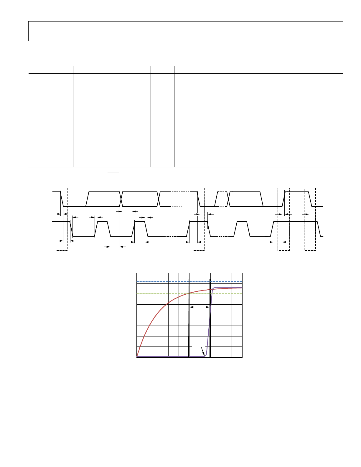
TIMING SPECIFICATIONS
Table 2. I2C Timing Parameters
Parameter Min Max Unit Description
f
0 400 kHz SCL clock frequency
SCL
t
0.6 Not applicable μs Hold time for a start condition
HD:STA
t
0.6 Not applicable μs Setup time for a repeated start condition
SU:STA
t
1.3 Not applicable μs Low period of the SCL clock
LOW
t
0.6 Not applicable μs High period of the SCL clock
HIGH
t
0 Not applicable μs Data hold time
HD:DAT
t
10 Not applicable ns Data setup time
SU:DAT
tR 1 300 ns Rise time for both SDA and SCL
tF 1 300 ns Fall time for both SDA and SCL
t
0.6 Not applicable μs Setup time for a stop condition
SU:STO
t
1 Not applicable ns Bus free time between a stop and a start condition
BUF
CIO 5 7 pF Capacitance for each I/O pin
t
10 Not applicable ns Reset pulse width1
RESET
1
Reset pulse width is defined as the time
SDA
RESET
is held below the logic low threshold (VIL) listed in Table 1 while the DVCC supply is within the operating range in Table 1.
t
t
HD:DAT
SU:DAT
t
R
t
HIGH
t
F
Figure 2. I
t
SU:STA
2
C Timing Diagram
t
HD:STA
t
SU:STO
t
R
t
BUF
SPSrS
07060-010
SCL
t
F
t
LOW
t
HD:STA
4.0
DVCC MAX LIMIT
3.5
DVCC MIN LIMIT
3.0
2.5
DVCC (V)
2.0
VOLTAGE (V)
1.5
1.0
0.5
0
0 5 10 15 20 25 30 35 40 45 50
Figure 3. Reset Timing Diagram
RESET
TIME (ns)
t
RESET
07060-103
Rev. B | Page 5 of 36
ADN8102
ABSOLUTE MAXIMUM RATINGS
Table 3.
Parameter Rating
VCC to VEE 3.7 V
V
V
TTI
V
V
TTO
Internal Power Dissipation 4.26 W
Differential Input Voltage 2.0 V
Logic Input Voltage VEE − 0.3 V < VIN < VCC + 0.6 V
Storage Temperature Range −65°C to +125°C
Lead Temperature 300°C
Junction Temperature 125°C
+ 0.6 V
CC
+ 0.6 V
CC
Stresses above those listed under Absolute Maximum Ratings
may cause permanent damage to the device. This is a stress rating
only; functional operation of the device at these or any other
conditions above those indicated in the operational section of
this specification is not implied. Exposure to absolute maximum
rating conditions for extended periods may affect device reliability.
ESD CAUTION
Rev. B | Page 6 of 36
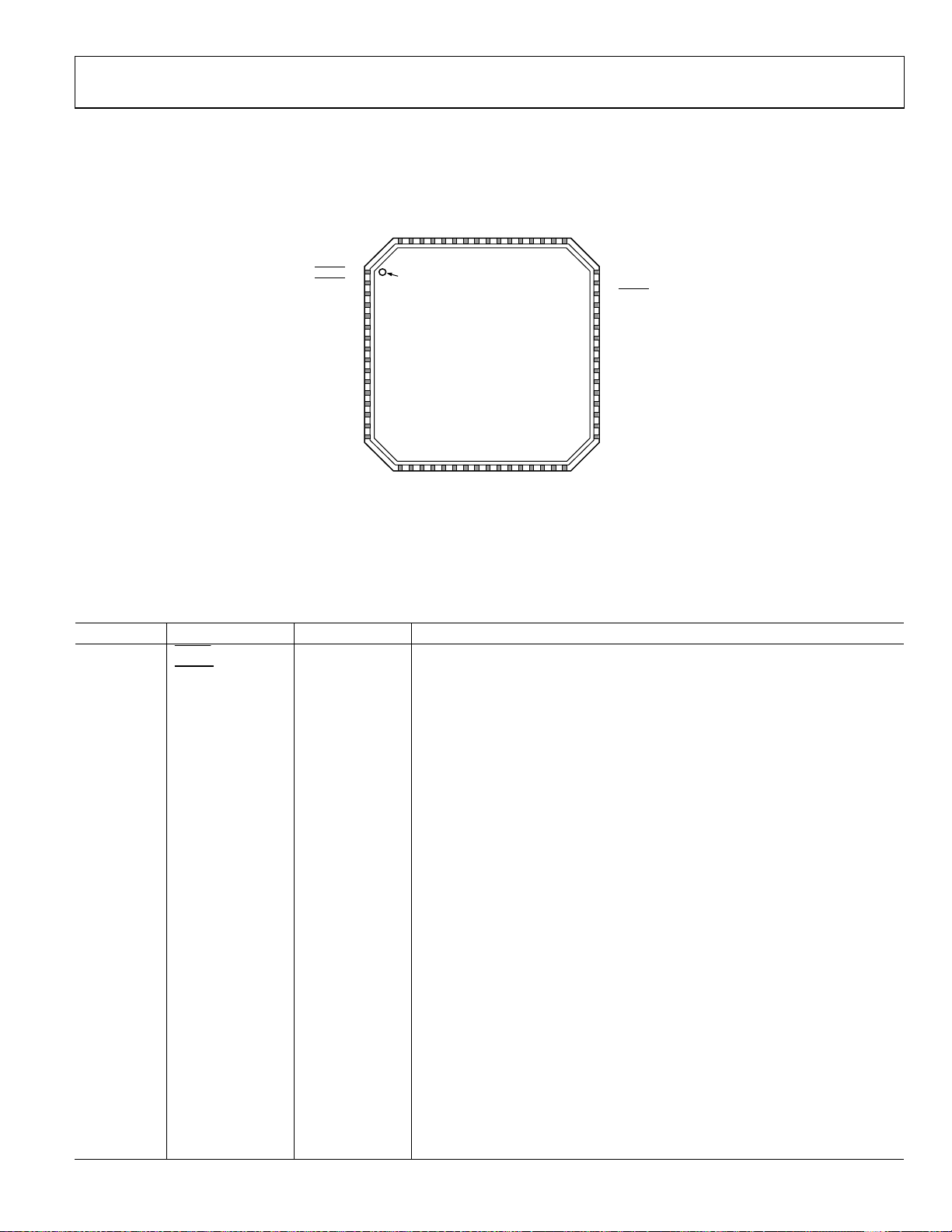
ADN8102
A
PIN CONFIGURATION AND FUNCTION DESCRIPTIONS
PE_A1
PE_A0
ENA
OP_A0
ON_A0
VCC
OP_A1
ON_A1
VTTO
OP_A2
ON_A2
VEE
OP_A3
ON_A3
ADDR1
646362616059585756555453525150
ADDR0
49
RESET
LOS_
IN_A0
IP_A0
VCC
IN_A1
IP_A1
VTTI
IN_A2
IP_A2
VEE
IN_A3
IP_A3
DVCC
EQ_A1
EQ_A0
PIN 1
1
INDICATO R
2
3
4
5
6
7
8
9
10
11
12
13
14
15
16
171819202122232425262728293031
VEE
NOTES
1. EXPOSE D PAD MUST BE CONNECT ED TO VEE.
LB
OP_B0
ON_B0
ADN8102
TOP VIEW
(Not to Scale)
VCC
VTTO
OP_B1
ON_B1
VEE
OP_B2
OP_B3
ON_B2
ON_B3
ENB
48
SCL
47
SDA
46
LOS_B
45
IP_B0
44
IN_B0
43
VCC
42
IP_B1
41
IN_B1
40
VTTI
39
IP_B2
38
IN_B2
37
VEE
36
IP_B3
35
IN_B3
34
EQ_B1
33
EQ_B0
32
PE_B1
PE_B0
Figure 4. Pin Configuration
Table 4. Pin Function Descriptions
Pin No. Mnemonic Type Description
1
2
RESET
LOS_A
Control Reset Input, Active Low
Digital I/O Port A Loss of Signal Status, Active Low
3 IN_A0 I/O High Speed Input Complement
4 IP_A0 I/O High Speed Input
5 VCC Power Positive Supply
6 IN_A1 I/O High Speed Input Complement
7 IP_A1 I/O High Speed Input
8 VTTI Power Input Termination Supply
9 IN_A2 I/O High Speed Input Complement
10 IP_A2 I/O High Speed Input
11 VEE Power Negative Supply
12 IN_A3 I/O High Speed Input Complement
13 IP_A3 I/O High Speed Input
14 DVCC Power Digital Power Supply
15 EQ_A1 Control Port A Input Equalization MSB
16 EQ_A0 Control Port A Input Equalization LSB
17 VEE Power Negative Supply
18 LB Control Loopback Control
19 ON_B0 I/O High Speed Output Complement
20 OP_B0 I/O High Speed Output
21 VCC Power Positive Supply
22 ON_B1 I/O High Speed Output Complement
23 OP_B1 I/O High Speed Output
24 VTTO Power Output Termination Supply
25 ON_B2 I/O High Speed Output Complement
26 OP_B2 I/O High Speed Output
27 VEE Power Negative Supply
Rev. B | Page 7 of 36
7060-002

ADN8102
Pin No. Mnemonic Type Description
28 ON_B3 I/O High Speed Output Complement
29 OP_B3 I/O High Speed Output
30 ENB Control Port B Enable
31 PE_B1 Control Port B Output Pre-Emphasis MSB
32 PE_B0 Control Port B Output Pre-Emphasis LSB
33 EQ_B0 Control Port B Input Equalization LSB
34 EQ_B1 Control Port B Input Equalization MSB
35 IN_B3 I/O High Speed Input Complement
36 IP_B3 I/O High Speed Input
37 VEE Power Negative Supply
38 IN_B2 I/O High Speed Input Complement
39 IP_B2 I/O High Speed Input
40 VTTI Power Input Termination Supply
41 IN_B1 I/O High Speed Input Complement
42 IP_B1 I/O High Speed Input
43 VCC Power Positive Supply
44 IN_B0 I/O High Speed Input Complement
45 IP_B0 I/O High Speed Input
46
47 SDA Control I2C Control Interface Data Input/Output
48 SCL Control I2C Control Interface Clock Input
49 ADDR0 Control I2C Control Interface Address LSB
50 ADDR1 Control I2C Control Interface Address MSB
51 ON_A3 I/O High Speed Output Complement
52 OP_A3 I/O High Speed Output
53 VEE Power Negative Supply
54 ON_A2 I/O High Speed Output Complement
55 OP_A2 I/O High Speed Output
56 VTTO Power Output Termination Supply
57 ON_A1 I/O High Speed Output Complement
58 OP_A1 I/O High Speed Output
59 VCC Power Positive Supply
60 ON_A0 I/O High Speed Output Complement
61 OP_A0 I/O High Speed Output
62 ENA Control Port A Enable
63 PE_A0 Control Port A Output Pre-Emphasis LSB
64 PE_A1 Control Port A Output Pre-Emphasis MSB
EP EPAD Power EPAD Must Be Connected to VEE
LOS_B
Digital I/O Port B Loss of Signal Status, Active Low
Rev. B | Page 8 of 36
ADN8102
V
V
V
V
TYPICAL PERFORMANCE CHARACTERISTICS
DATA OUT
PATTERN
GENERATOR
2 2
INPUT
PIN
ADN8102
AC-COUPL ED
EVALUATION
OUTPUT
BOARD
50Ω CABLES
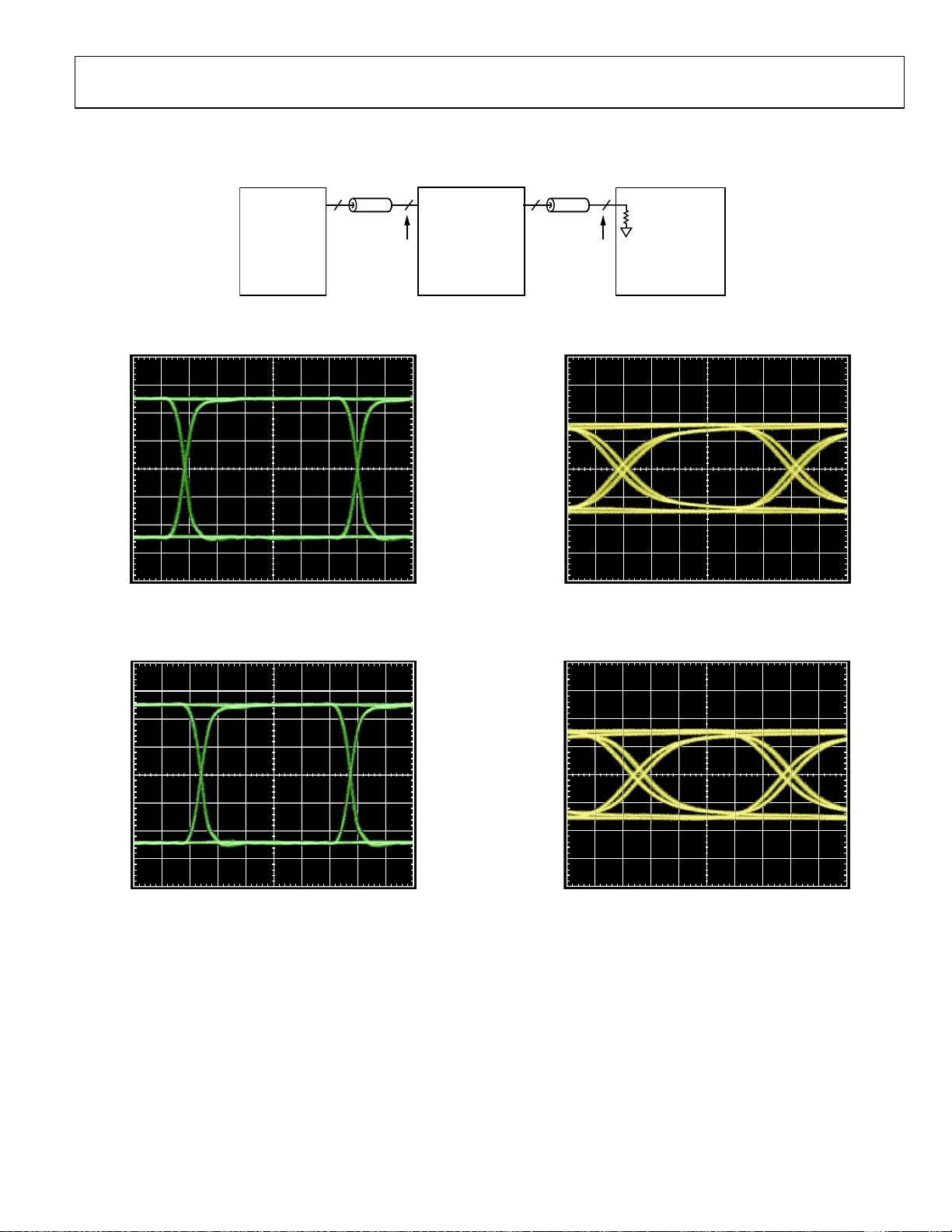
Figure 5. Standard Test Circuit (No Channel)
50Ω CABLES
2 2
PIN
50Ω
TP2TP1
OSCILLOSCOPE
HIGH SPEED
SAMPLING
07060-011
200mV/DI
50ps/DIV
07060-012
200mV/DI
50ps/DIV
Figure 6. 3.25 Gbps Input Eye (TP1 from Figure 5) Figure 8. 3.25 Gbps Output Eye, No Channel (TP2 from Figure 5)
200mV/DI
50ps/DIV
07060-013
200mV/DI
50ps/DIV
Figure 7. 3.75 Gbps Input Eye (TP1 from Figure 5) Figure 9. 3.75 Gbps Output Eye, No Channel (TP2 from Figure 5)
07060-014
07060-015
Rev. B | Page 9 of 36
ADN8102
V
V
V
V
V
50Ω CABLES
DATA OUT
PATTERN
200mV/DI
GENERATOR
2 2
FR4 TEST BACKPLANE
DIFFERENTIAL
STRIPLINE TRACES
TP1
8mils WIDE, 8mils SPACE,
8mils DIELECTRIC HEIGHT
TRACE LENGT HS = 40''
50Ω CABLES
2 2
TP2
INPUT
OUTPUT
PIN
ADN8102
AC-COUPLED
EVALUATION
BOARD
2 2
PIN
50Ω CABLES
50Ω
HIGH SPEED
TP3
SAMPLING
OSCILLOSCOPE
REFERENCE EYE DI AGRAM AT TP1
50ps/DIV
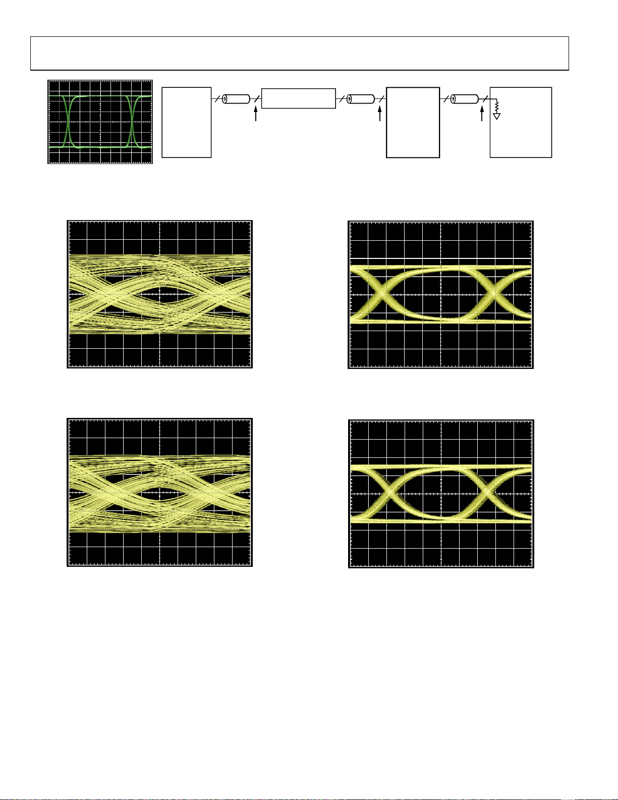
Figure 10. Input Equalization Test Circuit, FR4
200mV/DI
50ps/DIV
Figu re 11. 3. 25 Gbps I nput Eye, 40 Inch FR4 Input Channel (TP2 from Figure 10)
07060-017
200mV/DI
50ps/DIV
07060-019
Figure 13. 3.25 Gbps Output Eye, 40 Inch FR4 Input Channel, Best EQ Setting
(TP3 from Figure 10)
07060-016
200mV/DI
50ps/DIV
07060-018
Figu re 12. 3.75 Gb ps Input Eye, 40 Inch FR4 Input Channel (TP2 from Figure 10)
200mV/DI
50ps/DIV
07060-020
Figure 14. 3.75 Gbps Output Eye, 40 Inch FR4 Input Channel, Best EQ Setting
(TP3 from Figure 10)
Rev. B | Page 10 of 36
ADN8102
V
V
V
V
V
50Ω CABLES
DATA OUT
PATTERN
200mV/DI
GENERATOR
2 2
30m CX4 CABLE
TP1
50Ω CABLES
2 2
TP2
INPUT
OUTPUT
PIN
ADN8102
AC-COUPLED
EVALUATION
BOARD
2 2
PIN
50Ω CABLES
50Ω
HIGH SPEED
TP3
SAMPLING
OSCILLOSCOPE
REFERENCE EYE DI AGRAM AT TP1
50ps/DIV
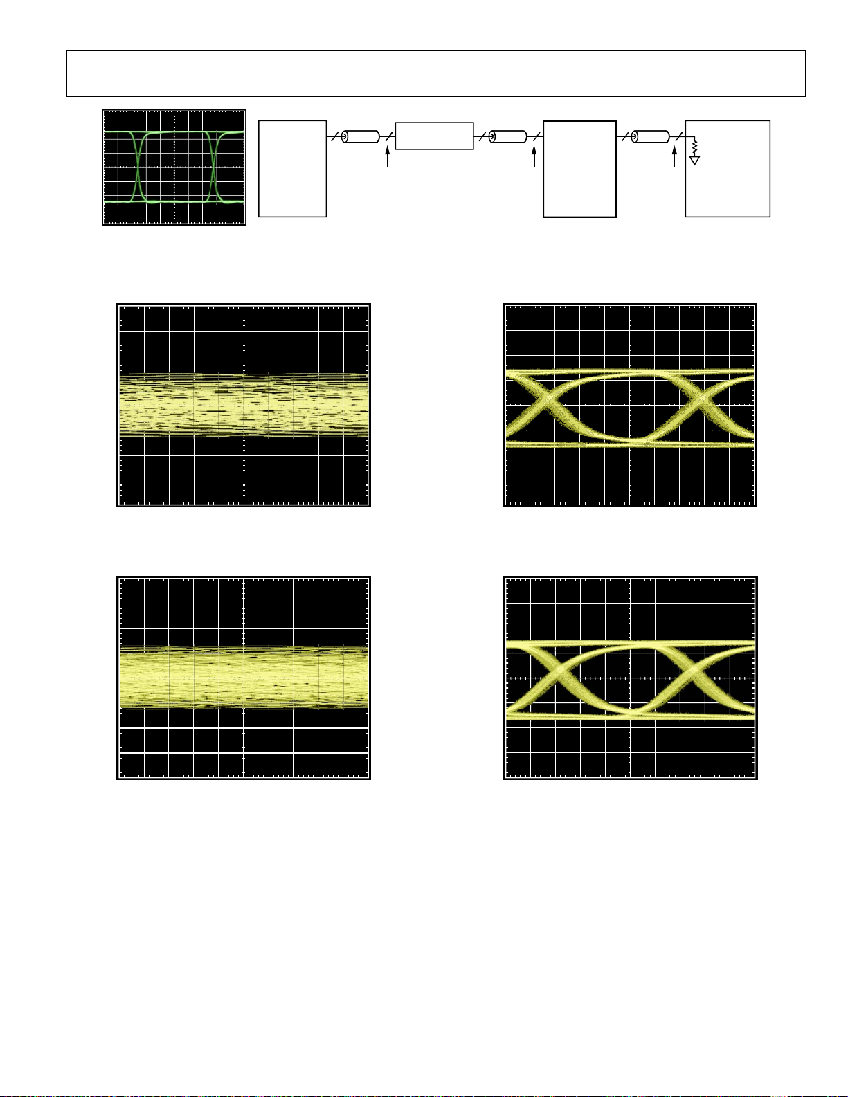
Figure 15. Input Equalization Test Circuit, CX4
200mV/DI
50ps/DIV
Figure 16. 3.25 Gbps Input Eye, 30 Meters CX4 Cable (TP2 from Figure 15)
07060-021
200mV/DI
07060-022
50ps/DIV
07060-024
Figure 18. 3.25 Gbps Output Eye, 30 Meters CX4 Cable, Best EQ Setting
(TP3 from Figure 15)
200mV/DI
50ps/DIV
07060-023
Figure 17. 3.75 Gbps Input Eye, 30 Meters CX4 Cable (TP2 from Figure 15)
200mV/DI
50ps/DIV
07060-025
Figure 19. 3.75 Gbps Output Eye, 30 Meters CX4 Cable, Best EQ Setting
(TP3 from Figure 15)
Rev. B | Page 11 of 36

ADN8102
V
V
V
V
V
50Ω CABLES
DATA OUT
2 2
PATTERN
GENERATOR
200mV/DI
TP1
INPUT
OUTPUT
PIN
ADN8102
AC-COUPLED
EVALUATION
BOARD
50Ω CABLES
2 2
PIN
FR4 TEST BACKPL ANE
DIFFERENTIAL
STRIPLINE TRACES
TP2
8mils WIDE, 8mils SPACE,
8mils DIELECTRIC HEIGHT
TRACE LENGTHS = 40''
50Ω CABLES
2 2
TP3
50Ω
HIGH SPEED
SAMPLING
OSCILLOSCOPE
REFERENCE EYE DI AGRAM AT TP1
50ps/DIV
200mV/DI
50ps/DIV
Figure 21. 3.25 Gbps Output Eye, 40 Inch FR4 Output Channel,
PE = 0 (TP3 from Figure 20)
Figure 20. Output Pre-Emphasis Test Circuit, FR4
200mV/DI
07060-027
Figure 23. 3.25 Gbps Output Eye, 40 Inch FR4 Output Channel,
50ps/DIV
PE = Best Setting (TP3 from Figure 20)
07060-026
07060-029
200mV/DI
50ps/DIV
Figure 22. 3.75 Gbps Output Eye, 40 Inch FR4 Output Channel,
PE = 0 (TP3 from Figure 20)
07060-028
200mV/DI
50ps/DIV
Figure 24. 3.75 Gbps Output Eye, 40 Inch FR4 Output Channel,
PE = Best Setting (TP3 from Figure 20)
07060-030
Rev. B | Page 12 of 36

ADN8102
V
V
V
V
V
50Ω CABLES
DATA OUT
22
PATTERN
GENERATOR
200mV/DI
TP1
INPUT
OUTPUT
PIN
ADN8102
AC-COUPLED
EVALUATION
BOARD
50Ω CABLES
22
PIN
TP2
15m CX4 CABLE
50Ω CABLES
22
50Ω
HIGH SPEED
TP3
SAMPLING
OSCILLOSCOPE
REFERENCE EYE DI AGRAM AT TP1
50ps/DIV
50mV/DI
Figure 26. 3.25 Gbps Output Eye, 15 Meters CX4 Cable,
50ps/DIV
PE = 0 (TP3 from Figure 25)
Figure 25. Output Pre-Emphasis Test Circuit, CX4
50mV/DI
07060-032
Figure 28. 3.25 Gbps Output Eye, 15 Meters CX4 Cable,
50ps/DIV
PE = Best Setting (TP3 from Figure 25)
07060-031
07060-034
50mV/DI
50ps/DIV
Figure 27. 3.75 Gbps Output Eye, 15 Meters CX4 Cable,
PE = 0 (TP3 from Figure 25)
07060-033
50mV/DI
50ps/DIV
Figure 29. 3.75 Gbps Output Eye, 15 Meters CX4 Cable,
PE = Best Setting (TP3 from Figure 25)
07060-035
Rev. B | Page 13 of 36

ADN8102
80
70
60
100
80
50
40
30
20
DETERMINISTIC JITTER (ps)
10
0
02040
DATA RATE (Hz)
Figure 30. Deterministic Jitter vs. Data Rate
100
90
80
70
60
50
40
30
DETERMINISTIC JITTER (ps)
20
10
0
0 0.5 1.0 1.5 2.0 2.5
DIFFERENTIAL INPUT SWING (V)
Figure 31. Deterministic Jitter vs. Differential Input Swing
60
07060-036
07060-037
60
40
DETERMINI STIC JIT TER (ps)
20
0
1.0 1.5 2.0 2. 5 3.0 3.5 4.0
VCC = 1.8V
VCC = 3.3V
INPUT COMMON MODE (V)
Figure 33. Deterministic Jitter vs. Input Common Mode
100
80
60
40
DETERMINI STIC JIT TER (ps)
20
0
1.0 1.5 2.0 2. 5 3.0 3.5 4.0
(V)
V
CC
Figure 34. Deterministic Jitter vs. Supply Voltage (VCC)
07060-039
07060-040
100
80
60
40
DETERMINI STIC JIT TER (ps)
20
0
–60 –40 –20 0 20 40 60 80 100
TEMPERATURE ( °C)
Figure 32. Deterministic Jitter vs. Temperature
07060-038
Rev. B | Page 14 of 36
100
80
60
40
DETERMINI STIC JIT TER (ps)
20
0
1.0 1.5 2.0 2. 5 3.0 3.5 4.0
V
TTO
VCC = 1.8V
VCC = 3.3V
(V)
Figure 35. Deterministic Jitter vs. Output Termination Voltage (V
TTO
07060-041
)

ADN8102
450000
400000
350000
300000
250000
200000
150000
NUMBER OF SAMPLES
100000
50000
0
–8 –6 –4 –2 0 2 4 6 8 10
JITTER ( ps)
07060-042
Figure 36. Random Jitter Histogram
100
90
80
(ps)
F
/t
R
t
70
60
50
–60 –40 –20 0 20 40 60 80 100
Figure 37. Rise Time (t
tR/t
F
TEMPERATURE ( °C)
)/Fall Time (tF) vs. Temperature
R
07060-043
Rev. B | Page 15 of 36

ADN8102
A
THEORY OF OPERATION
INTRODUCTION
The ADN8102 is a quad, bidirectional cable and backplane
equalizer that provides both input equalization and output preemphasis on both the line card and cable sides of the device.
The device supports full loopback and through connectivity
of the two unidirectional half-links, each consisting of four
differential signal pairs.
The ADN8102 offers extensively programmable output levels
and pre-emphasis as well as the ability to disable the output
current. The receivers integrate a programmable, multizero
equalizer transfer function that is optimized to compensate
either typical backplane or typical cable losses.
The I/O on-chip termination resistors are terminated to usersettable supplies to support dc coupling in a wide range of logic
styles. The ADN8102 supports a wide core supply range; V
can be set from 1.8 V to 3.3 V. These features, together with
programmable output levels, allow for a wide range of dc- and
ac-coupled I/O configurations.
The ADN8102 supports several control and configuration
modes, as shown in Tabl e 5. The pin control mode offers access
to a subset of the total feature list but allows for a much
simplified control scheme. The primary advantage of using the
serial control interface is that it allows finer resolution in setting
receive equalization, transmitter preemphasis, loss-of-signal
(LOS) behavior, and output levels.
By default, the ADN8102 starts in pin control mode. Strobing
RESET
the
pin sets all on-chip registers to their default values
and uses pins to configure loopback, PE, and EQ levels. In
Table 5. Control Interface Mode Register
Address Default Register Name Bit Bit Name Functionality Description
0x0F 0x00 Control 7:2 Reserved Set to 0.
interface mode 1:0 MODE[1:0] 00 = toggle pin control. Asynchronous control through toggle pins only.
11 = serial control. Register-based control through the I2C serial interface.
CC
01 = Loopback control via toggle pins, equalization, and preemphasis via
register-based control through the I2C serial interface.
10 = Equalization and preemphasis via toggle pins and loopback control
via register-based control through the I
mixed mode, loopback is still controlled through the external
pin. The user can override PE and EQ settings in mixed mode.
In serial mode, all functions are accessed through registers, and
the control pin inputs are ignored, except
The ADN8102 register set is controlled through a 2-wire, I
interface. The ADN8102 acts only as an I
slave address for the ADN8102 I
2
C interface contains the static
RESET
.
2
2
C slave device. The 7-bit
C
value b10010 for the upper four bits. The lower two bits are
controlled by the input pins, ADDR[1:0]
LOS_B
Ix_B[3:0]
Ox_A[3:0]
DDR[1:0]
SCL
SDA
RESET
RECEIVE
EQUALIZATION
EQ
LB
TRANSMIT
PRE-EMPHASIS
PE
Figure 38. Simplified Functional Block Diagram
ADN8102
2:1
CONTROL LO GIC
TRANSMIT
PRE-EMPHASIS
2:1
RECEIVE
EQUALIZATION
PE
EQ
Ox_B[3:0]
LOS_A
Ix_A[3:0]
EQ_A[1:0]
PE_A[1:0]
EQ_B[1:0]
PE_B[1:0]
ENA
ENB
2
C serial interface.
07060-003
Rev. B | Page 16 of 36

ADN8102
V
RECEIVERS
Input Structure and Input Levels
The ADN8102 receiver inputs incorporate 50 Ω termination
resistors, ESD protection, and a multizero transfer function
equalizer that can be optimized for backplane or cable operation.
Each channel also provides a programmable LOS function that
provides an interrupt that can be used to squelch or disable the
associated output when the differential input voltage falls below the
programmed threshold value. Each receive channel also provides a
P/N inversion function that allows the user to swap the sign of
the input signal path to eliminate the need for board-level
crossovers in the receiver channel.
Tabl e 6 illustrates some, but not all, possible combinations of
input supply voltages.
Table 6. Common Input Voltage Levels
Configuration VCC (V) V
Low V
, ac-coupled input 1.8 1.6
TTI
(V)
TTI
Single 1.8 V supply 1.8 1.8
3.3 V core 3.3 1.8
Single 3.3 V supply 3.3 3.3
V
CC
TTI
IP
IN
V
EE
SIMPLI FIED REC EIVER INPUT CIRCUI T
R1
R2
RLN RLP
Q1
R3
1kΩ
RP
52Ω
Figure 39. Simplified Input Structure
RN
52Ω
750Ω
750Ω
Q2
I1
EQUALIZATION SETTINGS
The ADN8102 receiver incorporates a multizero transfer function,
continuous time equalizer that provides up to 22 dB of high
frequency boost at 1.875 GHz to compensate up to 30 meters
of CX4 cable or 40 inches of FR4 at 3.75 Gbps. The ADN8102
allows joint control of the equalizer transfer function of the
four equalizer channels in a single port through the I
interface. Port A and Port B equalizer transfer functions are
controlled via Register 0x80 and Register 0xA0, respectively.
The equalizer transfer function allows independent control of
the boost in two different frequency ranges for optimal matching
with the loss shape of the user’s channel (for example, skin-effect
loss dominated or dielectric loss dominated). By default, the
equalizer control is simplified to two independent look up
tables (LUT) of basic settings that provide nine settings, each
optimized for CX4 cable and FR4 to ease programming for
2
C control
07060-004
typical channels. The default state of the part selects the CX4
optimized equalization map for the IN_A[3:0] channels that
interface with the cable and the FR4 optimized equalization map
for the IN_B[3:0] channels that interface with the board. Full
control of the equalizer is available via the I
2
C control interface by
writing MODE[0] = 1 at Address 0x0F. Ta b l e 8 summarizes the
high frequency boost for each of the basic control settings and
the typical length of CX4 cable and FR4 trace that each setting
compensates. Setting the EQBY bit of the IN_A/IN_B configuration
registers high sets the equalization to 1.5 dB of boost, which
compensates 0 meters to 2 meters of CX4 or 0 inches to
5 inches of FR4.
Setting the LUT SELECT bit = 1 (Bit 1 in the IN_Ax/IN_Bx FR4
control registers) allows the default map selection (CX4 or FR4
optimized) to be overwritten via the LUT FR4/CX4 bit (Bit 0)
in the IN_Ax/IN_Bx FR4 control registers. Setting this bit high
selects the FR4 optimized map, and setting it low selects the CX4
optimized map. These settings are set on a per channel basis
(see Tabl e 9 and Ta b le 2 2 ).
Table 7.
LUT SELECT LUT FR4/CX4 Description
0 (default) X1
Port A eq optimized for CX4
cable
Port B eq optimized for FR4
PCB trace
1 0 Eq optimized for CX4 cable
1 1 Eq optimized for FR4 PCB trace
1
X = don’t care.
Advanced Equalization Settings
The user can also specify the boost in the midfrequency and high
frequency ranges independently. This is done by writing to the
IN_A/IN_B EQ1 control and IN_A/IN_B EQ2 control registers for
the channel of interest. Each of these registers provides 32 settings
of boost, with IN_A/IN_B EQ1 control setting the midfrequency
boost and IN_A/IN_B EQ2 control setting the high frequency
boost. The IN_A/IN_B EQx control registers are ordered such
that Bit 5 is a sign bit, and midlevel boost is centered on 0x00;
setting Bit 5 low and increasing the LSBs results in decreasing
boost, while setting Bit 5 high and increasing the LSBs results in
increasing boost. The EQ CTL SRC bit (Bit 6) in the IN_A/IN_B
EQ1 control registers determines whether the equalization
control for the channel of interest is selected from the optimized
map or directly from the IN_A/IN_B EQx control registers (per
port). Setting this bit high selects equalization control directly
from the IN_A/IN_B EQx control registers, and setting it low
selects equalization control from the selected optimized map.
Rev. B | Page 17 of 36

ADN8102
Table 8. Receive Equalizer Boost vs. Setting (CX4 and FR4 Optimized Maps)
IN_Ax/IN_Bx
EQ_A[1:0] and
EQ_B[1:0] Pins
X
0 0 0 10 2 to 6 3.5 5 to 10
1 0 12 8 to 10 3.9 10 to 15
1 2 0 14 12 to 14 4.25 15 to 20
3 0 17 16 to 18 4.5 20 to 25
4 0 19 20 to 22 4.75 25 to 30
2 5 0 20 24 to 26 5.0 30 to 35
6 0 21 28 to 30 5.3 35 to 40
3 7 0 22 30 to 32 5.5 35 to 40
1
X = Don’t care
Configuration,
EQ[2:0]
1
1 1.5 < 2 1.5 < 5
Table 9. Receive Configuration and Equalization Registers
Name Address Bit 7 Bit 6 Bit 5 Bit 4 Bit 3 Bit 2 Bit 1 Bit 0 Default
IN_A/IN_B
configuration
IN_A/IN_B
EQ1 control
IN_A/IN_B
EQ2 control
IN_Ax/IN_Bx
FR4 control
0x80, 0xA0 PNSWAP EQBY EN EQ[2] EQ[1] EQ[0] 0x30
0x83, 0xA3 EQ CTL SRC EQ1[5] EQ1[4] EQ1[3] EQ1[2] EQ1[1] EQ1[0] 0x00
0x84, 0xA4 EQ2[5] EQ2[4] EQ2[3] EQ2[2] EQ2[1] EQ2[0] 0x00
0x85, 0x8D, 0x95,
0x9D, 0xA5, 0xAD,
0xB5, 0xBD
Loss of Signal/Signal Detect
An independent signal detect output is provided for all eight
input ports of the device. The signal-detect function measures
the low frequency amplitude of the signal at the receiver input
and compares this measurement with a defined threshold level.
If the measurement indicates that the input signal swing is
smaller than the threshold for 250 μs, the channel indicates a
loss-of-signal event. Assertion and deassertion of the LOS signal
occurs within 100 μs of the event.
The LOS-assert and LOS-deassert levels are set on a per channel
basis through the I
2
C control interface, by writing to the IN_A/
IN_B LOS threshold and IN_A/IN_B LOS hysteresis registers,
respectively. The recommended settings are IN_A/IN_B LOS
threshold = 0x0C and IN_A/IN_B LOS hysteresis = 0x0D.
All ports are factory tested with these settings to ensure that an
LOS event is asserted for single-ended dc input swings less than
20 mV and is deasserted for single-ended dc input swings greater
than 225 mV.
The LOS status for each individual channel can be accessed
through the I
2
C control interface. The independent channel
LOS status can be read from the IN_A/IN_B LOS status registers
(Address 0x1F and Address 0x3F). The four LSBs of each register
represent the current LOS status of each channel, with high
representing an ongoing LOS event. The four MSBs of each
Cable Optimized FR4 Optimized
Typical CX4 Cable
EQBY Boost (dB)
LUT SELECT LUT FR4/CX4 0x00
Length (Meters) Boost (dB)
Typical FR4 Trace
Length (Inches)
register represent the historical LOS status of each channel,
with high representing a LOS event at any time on a specific
channel. The MSBs are sticky and remain high once asserted
until cleared by the user by overwriting the bits to 0.
Recommended LOS Settings
Recommended settings for LOS are as follows:
• Set IN_A/IN_B LOS threshold to 0x0C for an assert
voltage of 20 mV differential (40 mV p-p differential).
• Set IN_A/IN_B LOS hysteresis to 0x0D for a deassert voltage
of 225 mV differential (450 mV p-p differential).
LANE INVERSION
The input P/N inversion is a feature intended to allow the user
to implement the equivalent of a board-level crossover in a much
smaller area and without additional via impedance discontinuities
that degrade the high frequency integrity of the signal path. The
P/N inversion is available on a per port basis and is controlled
through the I
plished by writing to the PNSWAP bit (Bit 6) of the IN_A/IN_B
configuration register (see Tabl e 9) with low representing a
noninverting configuration and high representing an inverting
configuration. Note that using this feature to account for signal
inversions downstream of the receiver requires additional attention
when switching connectivity.
2
C control interface. The P/N inversion is accom-
Rev. B | Page 18 of 36

ADN8102
Table 10. LOS Threshold and Hysteresis Control Registers
Name Address Bit 7 Bit 6 Bit 5 Bit 4 Bit 3 Bit 2 Bit 1 Bit 0 Default
IN_A/IN_B
LOS threshold
IN_A/IN_B
LOS hysteresis
0x81,
0xA1
0x82,
0xA2
Table 11. LOS Status Registers
Name Address Bit 7 Bit 6 Bit 5 Bit 4 Bit 3 Bit 2 Bit 1 Bit 0
IN_A/IN_B
LOS status
0x1F,
0x3F
THRESH[6] THRESH[5] THRESH[4] THRESH[3] THRESH[2] THRESH[1] THRESH[0] 0x04
HYST[6] HYST[5] HYST[4] HYST[3] HYST[2] HYST[1] HYST[0] 0x12
STICKY
LOS[3]
STICKY
LOS[2]
STICKY
LOS[1]
STICKY LOS[0]
REAL-TIME
LOS[3]
REAL-TIME
LOS[2]
REAL-TIME
LOS[1]
REAL-TIME
LOS[0]
Rev. B | Page 19 of 36

ADN8102
A
LOOPBACK
The ADN8102 provides loopback on both input ports (Port A:
cable interface input, and Port B: line card interface input). The
external loopback toggle pin, LB, controls the loopback of the Port
B input only (board side loopback). When loopback is asserted,
valid data continues to pass through the Port B link, but the
Port B input signals are also shunted to the Port A output to allow
testing and debugging without disrupting valid data. This
loopback, as well as loopback of the Port A input (cable side
loopback), can be programmed through the I
loopbacks are controlled through the I
Bit 0 and Bit 1 of the loopback control register (Register 0x02).
CABLE SIDE LOO PBACK BOARD SIDE LOOPBACK FULL LO OPBACK
Ix_B[3:0]
Ox_A[3:0]
LB
RECEIVE
EQUALIZATION
EQ
TRANSMIT
PRE-EMPHASIS
PE
TRANSMIT
PRE-EMPHASIS
PE
RECEIVE
EQUALIZATION
EQ
Ox_B[3:0]
LOS_A
Ix_A[3:0]
2
C interface. The
2
C interface by writing to
RECEIVE
EQUALIZATION
Ix_B[3:0]
Ox_A[3:0]
LB
EQ
TRANSMIT
PRE-EMPHASIS
PE
Bit 0 represents loopback of the Port A inputs to the Port B
outputs (cable side loopback). Bit 1 represents loopback of the
Port B inputs to the Port A outputs (board side loopback), with
high representing loopback for both bits. Bit 1 can be overridden
by the LB pin if the pin mode register is set to enable loopback
via external pin as shown in Ta b le 5 . Both input ports can be
looped back simultaneously (full loopback) by writing high to
both Bit 0 and Bit 1, but in this case, valid data is disrupted on
each channel. Figure 40 illustrates the three loopback modes.
TRANSMIT
PRE-EMPHASIS
PE
RECEIVE
EQUA LIZATION
EQ
Ox_B[3:0 ]
LOS_A
Ix_A[3:0]
Ix_B[3:0]
Ox_A[3:0 ]
LB
RECEIVE
EQUALIZATION
EQ
TRANSMIT
PRE-EMPHASIS
PE
TRANSMIT
PRE-EMPHASIS
PE
RECEIVE
EQUALIZATION
EQ
Ox_B[3:0]
LOS_A
Ix_A[3:0]
DDR[1:0]
SCL
SDA
RESET
CONTROL LOGIC
EQ_A[1:0]
PE_A[1:0]
EQ_B[1:0]
PE_B[1:0]
ENA
ENB
ADDR[1:0]
SCL
SDA
RESET
CONTROL LOGIC
EQ_A[1:0]
PE_A [1:0]
EQ_B[1:0]
PE_B [1:0]
ENA
ENB
ADDR[1:0]
SCL
SDA
RESET
CONTROL LOGIC
EQ_A[1:0]
PE_A[1:0]
EQ_B[1:0]
PE_B[1:0]
ENA
ENB
07060-005
Figure 40. Loopback Modes of Operation
Table 12. Loopback Control Functionality
Control Mode1 LB Pin LB[1] LB[0] Description
Pin Control (00 or 01) 0 X2 X Loopback disabled
1 X X Board side loopback enabled
Serial Control X 0 0 Loopback disabled
(10 or 11) X 0 1 Cable side loopback enabled
X 1 0 Board side loopback enabled
X 1 1 Full loopback enabled
1
Refer to Table 5 for additional information regarding control mode settings.
2
X = don’t care.
Table 13. Loopback Control Register
Name Address Bit 7 Bit 6 Bit 5 Bit 4 Bit 3 Bit 2 Bit 1 Bit 0 Default
Loopback control 0x02 LB[1] LB[0] 0x00
Rev. B | Page 20 of 36

ADN8102
TRANSMITTERS
Output Structure and Output Levels
The ADN8102 transmitter outputs incorporate 50 Ω termination resistors, ESD protection, and an output current switch. Each
port provides control of both the absolute output level and the
pre-emphasis output level. It should be noted that the choice of
output level affects the output common-mode level. A 600 mV
peak-to-peak differential output level with full pre-emphasis
range requires an output termination voltage of 2.5 V or greater
(V
, VCC ≥ 2.5 V).
TTO
Tx SIMPLIFIED DIAGRAM
V3
VC
V2
VP
V1
VN
Figure 41. Simplified Output Structure
ON-CHIP
TERMINATION
RP
50Ω
Q1
+ I
I
DC
PE
ESD
RN
50Ω
Q2
I
TOT
Pre-Emphasis
The total output amplitude and pre-emphasis setting space is
reduced to a single map of basic settings that provide seven
settings of output equalization to ease programming for typical
channels. The PE_A/PE_B[1:0] pins provide selections 0, 2, 4,
and 6 of the seven pre-emphasis settings through toggle pin
control, covering the entire range of settings at lower resolution.
The full resolution of seven settings is available through the I
interface by writing to Bits[2:0] (PE[2:0] of the OUT_A/OUT_B
configuration registers) with I
2
C settings overriding the toggle
V
V
OP
ON
V
CC
TTO
EE
2
C
07060-006
pin control. Similar to the receiver settings, the ADN8102 allows
joint control of all four channels in a transmit port. Tab l e 15
summarizes the absolute output level, pre-emphasis level, and
high frequency boost for each of the basic control settings and
the typical length of the CX4 cable and FR4 trace that each
setting compensates.
Full control of the transmit output levels is available through the
2
I
C control interface. This full control is achieved by writing to
the OUT_A/OUT_B Output Level Control[1:0] registers for the
channel of interest. Tab le 1 7 shows the supported output level
settings of the OUT_A/OUT_B Output Level Control[1:0]
registers. Register settings not listed in Tab l e 1 7 are not
supported by the ADN8102.
The output equalization is optimized for less than 1.75 Gbps
operation but can be optimized for higher speed applications at
up to 3.75 Gbps through the I
2
C control interface by writing to
the DATA RATE bit (Bit 4) of the OUT_A/OUT_B configuration
registers, with high representing 3.75 Gbps and low representing
1.75 Gbps. The PE CTL SRC bit (Bit 7) in the OUT_A/OUT_B
Output Level Control 1 register determines whether the preemphasis and output current controls for the channel of interest
are selected from the optimized map or directly from the OUT_A/
OUT_B Output Level Control[1:0] registers (per channel). Setting
this bit high selects pre-emphasis control directly from the
OUT_A/OUT_B Output Level Control[1:0] registers, and setting
it low selects pre-emphasis control from the optimized map.
Table 14. Data Rate Select
OUT_A/OUT_B Configuration Bit 4 Supported Data Rates
0 (default) 0 Gbps to 1.75 Gbps
1 1.75 Gbps to 3.75 Gbps
Table 15. Transmit Pre-Emphasis Boost and Overshoot vs. Setting
PE[2:0] Register PE[1:0] Pins Boost (dB) Overshoot (%)
DC Swing
(mV p-p diff)
Typical CX4 Cable
Length (Meters)
Typical FR4 Trace
Length (Inches)
0 0 0 0 800 0 to 2.5 0 to 5
1 Not applicable 2 25 800 2.5 to 5 0 to 5
2 1 3.5 50 800 5 to 7.5 10 to 15
3 Not applicable 4.9 75 800 7.5 to 10 10 to 15
4 2 6 100 800 10 to 12.5 15 to 20
5 Not applicable 7.4 133 600 15 to 17.5 20 to 25
6 4 9.5 200 400 20 to 22.5 25 to 30
Table 16. Output Configuration Registers
Name Address Bit 7 Bit 6 Bit 5 Bit 4 Bit 3 Bit 2 Bit 1 Bit 0 Default
OUT_A/OUT_B configuration 0xC0, 0xE0 EN DATA RATE PE[2] PE[1] PE[0] 0x20
OUT_A/OUT_B Output Level Control 1 0xC1, 0xE1 PE CTL SRC OUTx_OLEV1[6:0] 0x40
OUT_A/OUT_B Output Level Control 0 0xC2, 0xE2 OUTx_OLEV0[6:0] 0x40
Rev. B | Page 21 of 36

ADN8102
Table 17. Output Level Settings
V
(mV) V
SW-DC
50 50 100 100 0.00 2 0x00 0x81
50 150 100 300 9.54 6 0x11 0x81
50 250 100 500 13.98 10 0x22 0x81
50 350 100 700 16.90 14 0x33 0x81
50 450 100 900 19.08 18 0x44 0x81
50 550 100 1100 20.83 22 0x55 0x81
50 650 100 1300 22.28 26 0x66 0x81
100 100 200 200 0.00 4 0x00 0x91
100 200 200 400 6.02 8 0x11 0x91
100 300 200 600 9.54 12 0x22 0x91
100 400 200 800 12.04 16 0x33 0x91
100 500 200 1000 13.98 20 0x44 0x91
100 600 200 1200 15.56 24 0x55 0x91
100 700 200 1400 16.90 28 0x66 0x91
150 150 300 300 0.00 6 0x00 0x92
150 250 300 500 4.44 10 0x11 0x92
150 350 300 700 7.36 14 0x22 0x92
150 450 300 900 9.54 18 0x33 0x92
150 550 300 1100 11.29 22 0x44 0x92
150 650 300 1300 12.74 26 0x55 0x92
150 750 300 1500 13.98 30 0x66 0x92
200 200 400 400 0.00 8 0x00 0xA2
200 300
200 400
200 500
200 600
200 700
200 800
250 250 500 500 0.00 10 0x00 0xA3
250 350 500 700 2.92 14 0x11 0xA3
250 450 500 900 5.11 18 0x22 0xA3
250 550 500 1100 6.85 22 0x33 0xA3
250 650 500 1300 8.30 26 0x44 0xA3
250 750 500 1500 9.54 30 0x55 0xA3
250 850 500 1700 10.63 34 0x66 0xA3
300 300 600 600 0.00 12 0x00 0xB3
300 400 600 800 2.50 16 0x11 0xB3
300 500 600 1000 4.44 20 0x22 0xB3
300 600 600 1200 6.02 24 0x33 0xB3
300 700 600 1400 7.36 28 0x44 0xB3
300 800 600 1600 8.52 32 0x55 0xB3
300 900 600 1800 9.54 36 0x66 0xB3
350 350 700 700 0.00 14 0x00 0xB4
350 450 700 900 2.18 18 0x11 0xB4
350 550 700 1100 3.93 22 0x22 0xB4
350 650 700 1300 5.38 26 0x33 0xB4
350 750 700 1400 6.62 30 0x44 0xB4
350 850 700 1700 7.71 34 0x55 0xB4
350 950 700 1900 8.67 38 0x66 0xB4
400 400 800 800 0.00 16 0x00 0xC4
400 500 800 1000 1.94 20 0x11 0xC4
400 600 800 1200 3.52 24 0x22 0xC4
400 700 800 1400 4.86 28 0x33 0xC4
400 800 800 1600 6.02 32 0x44 0xC4
400 900 800 1800 7.04 36 0x55 0xC4
400 1000 800 2000 7.96 40 0x66 0xC4
SW-PE
(mV) V
DPP-DC
400
400
400
400
400
400
(mV) V
(mV) PE (dB) I
DPP-PE
(mA) OUT_A/OUT_B OLEV 0 OUT_A/OUT_B OLEV 1
TOT
600 3.52 12 0x11 0xA2
800 6.02 16 0x22 0xA2
1000 7.96 20 0x33 0xA2
1200 9.54 24 0x44 0xA2
1400 10.88 28 0x55 0xA2
1600 12.04 32 0x66 0xA2
Rev. B | Page 22 of 36

ADN8102
V
(mV) V
SW-DC
450 450 900 900 0.00 18 0x00 0xC5
450 550 900 1100 1.74 22 0x11 0xC5
450 650 900 1300 3.19 26 0x22 0xC5
450 750 900 1500 4.44 30 0x33 0xC5
450 850 900 1700 5.52 34 0x44 0xC5
450 950 900 1900 6.49 38 0x55 0xC5
450 1050 900 2100 7.36 42 0x66 0xC5
500 500 1000 1000 0.00 20 0x00 0xD5
500 600 1000 1200 1.58 24 0x11 0xD5
500 700 1000 1400 2.92 28 0x22 0xD5
500 800 1000 1600 4.08 32 0x33 0xD5
500 900 1000 1800 5.11 36 0x44 0xD5
500 1000 1000 2000 6.02 40 0x55 0xD5
500 1100 1000 2200 6.85 44 0x66 0xD5
550 550 1100 1100 0.00 22 0x00 0xD6
550 650 1100 1300 1.45 26 0x11 0xD6
550 750 1100 1500 2.69 30 0x22 0xD6
550 850 1100 1700 3.78 34 0x33 0xD6
550 950 1100 1900 4.75 38 0x44 0xD6
550 1050 1100 2100 5.62 42 0x55 0xD6
550 1150 1100 2300 6.41 46 0x66 0xD6
600 600 1200 1200 0.00 24 0x00 0xE6
600 700 1200 1400 1.34 28 0x11 0xE6
600 800 1200 1600 2.50 32 0x22 0xE6
600 900 1200 1800 3.52 36 0x33 0xE6
600 1000 1200 2000 4.44 40 0x44 0xE6
600 1100 1200 2200 5.26 44 0x55 0xE6
600 1200 1200 2400 6.02 48 0x66 0xE6
650 650 1300 1300 0.00 26 0x01 0xE6
650 750 1300 1500 1.24 30 0x12 0xE6
650 850 1300 1700 2.33 34 0x23 0xE6
650 950 1300 1900 3.30 38 0x34 0xE6
650 1050 1300 2100 4.17 42 0x45 0xE6
650 1150 1300 2300 4.96 46 0x56 0xE6
700 700 1400 1400 0.00 28 0x02 0xE6
700 800 1400 1600 1.16 32 0x13 0xE6
700 900 1400 1800 2.18 36 0x24 0xE6
700 1000 1400 2000 3.10 40 0x35 0xE6
700 1100 1400 2300 3.93 44 0x46 0xE6
750 750 1500 1500 0.00 30 0x03 0xE6
750 850 1500 1700 1.09 34 0x14 0xE6
750 950 1500 1900 2.05 38 0x25 0xE6
750 1050 1500 2100 2.92 42 0x36 0xE6
800 800 1600 1600 0.00 32 0x04 0xE6
800 900 1600 1800 1.02 36 0x15 0xE6
800 1000 1600 2000 1.94 40 0x26 0xE6
850 850 1700 1700 0.00 34 0x05 0xE6
850 950 1700 1900 0.97 38 0x16 0xE6
900 900 1800 1800 0.00 36 0x06 0xE6
SW-PE
(mV) V
(mV) V
DPP-DC
(mV) PE (dB) I
DPP-PE
(mA) OUT_A/OUT_B OLEV 0 OUT_A/OUT_B OLEV 1
TOT
Rev. B | Page 23 of 36

ADN8102
SELECTIVE SQUELCH AND DISABLE
Each transmitter is equipped with output disable and output
squelch controls. Disable is a full power-down state: the transmitter current is reduced to zero, and the output pins pull up
to V
, but there is a delay of approximately 1 μs associated
TTO
with re-enabling the transmitter. The output disable control is
accessed through the EN bit (Bit 4) of the OUT_A/OUT_B
configuration registers through the I
Squelch is not a full power-down state but a state in which only
the output current is reduced to zero and the output pins pull
up to V
, and there is a much smaller delay to bring back the
TTO
output current. The output squelch and the output disable control
can both be accessed through the OUT_A/OUT_B squelch
control registers, with the top nibble representing the squelch
control for one entire output port, and the bottom nibble
representing the output disable for one entire output port. The
ports are disabled or squelched by writing 0s to the corresponding
nibbles. The ports are enabled by writing all 1s, which is the
2
C control interface.
default setting. For example, to squelch Port A, Register 0xC3
must be set to 0x0F. The entire nibble must be written to all 0s
for this functionality.
Table 18. Squelch and Disable Control Registers
Name Address Data Default
OUT_A/
OUT_B
squelch
control
0xC3,
0xE3
SQUELCH[3:0] DISABLE[3:0]
0xFF
Table 19. Squelch and Disable Functionality
SQUELCH[3:0]
1111 1111 Enabled (default)
xxxx1 0000 Disabled
0000 1111 Squelched
1
xxxx = don’t care
DISABLE[3:0]
Output State
Rev. B | Page 24 of 36

ADN8102
G
I2C CONTROL INTERFACE
SERIAL INTERFACE GENERAL FUNCTIONALITY
The ADN8102 register set is controlled through a 2-wire
2
C interface. The ADN8102 acts only as an I2C slave device.
I
Therefore, the I
master to configure the ADN8102 and other I
2
C bus in the system needs to include an I2C
2
C devices that
may be on the bus. Data transfers are controlled using the two
2
I
C wires: the SCL input clock pin and the SDA bidirectional
data pin.
The ADN8102 I
2
C interface can be run in the standard (100 kHz)
and fast (400 kHz) modes. The SDA line only changes value
when the SCL pin is low with two exceptions. To indicate the
beginning or continuation of a transfer, the SDA pin is driven
low while the SCL pin is high, and to indicate the end of a
transfer, the SDA line is driven high while the SCL line is high.
Therefore, it is important to control the SCL clock to toggle
only when the SDA line is stable, unless indicating a start,
repeated start, or stop condition.
I2C INTERFACE DATA TRANSFERS—DATA WRITE
To write data to the ADN8102 register set, a microcontroller, or
any other I
to the ADN8102 slave device. The steps that need to be completed
are listed as follows, where the signals are controlled by the I
master, unless otherwise specified. A diagram of the procedure
can be seen in Figure 42.
1. Send a start condition (while holding the SCL line high,
2. Send the ADN8102 part address (seven bits) whose upper
3. Send the write indicator bit (0).
4. Wait for the ADN8102 to acknowledge the request.
5. Send the register address (eight bits) to which data is to be
6. Wait for the ADN8102 to acknowledge the request.
2
C master, needs to send the appropriate control signals
2
C
pull the SDA line low).
five bits are the static value 10010b and whose lower two
bits are controlled by the ADDR[1:0] input pins. This transfer
should be MSB first.
written. This transfer should be MSB first.
7. Send the data (eight bits) to be written to the register whose
address was set in Step 5. This transfer should be MSB first.
8. Wait for the ADN8102 to acknowledge the request.
9a. Send a stop condition (while holding the SCL line high,
pull the SDA line high) and release control of the bus.
9b. Send a repeated start condition (while holding the SCL line
high, pull the SDA line low) and continue with Step 2 in
this procedure to perform another write.
9c. Send a repeated start condition (while holding the SCL line
high, pull the SDA line low) and continue with Step 2 of
the read procedure (in the I2C Interface Data Transfers—
Data Read section) to perform a read from another address.
9d. Send a repeated start condition (while holding the SCL line
high, pull the SDA line low) and continue with Step 8 of
the read procedure (in the I2C Interface Data Transfers—
Data Read section) to perform a read from the same
address set in Step 5.
Figure 42 shows the ADN8102 write process. The SCL signal is
shown along with a general write operation and a specific example.
In the example, Data 0x92 is written to Address 0x6D of an
ADN8102 part with a part address of 0x4B. The part address is
seven bits wide. The upper five bits of the ADN8102 are internally
set to 10010b. The lower two bits are controlled by the ADDR[1:0]
pins. In this example, the bits controlled by the ADDR[1:0] pins
are set to 11b. In Figure 42, the corresponding step number is
visible in the circle under the waveform. The SCL line is driven by
2
the I
C master and never by the ADN8102 slave. As for the SDA
line, the data in the shaded polygons is driven by the ADN8102,
whereas the data in the nonshaded polygons is driven by the I
2
C
master. The end phase case shown is that of Step 9a.
Note that the SDA line only changes when the SCL line is low,
except for the case of sending a start, stop, or repeated start
condition, Step 1 and Step 9 in this case.
SCL
ENERAL CASE
SDA
EXAMPLE
SDA
START REGISTER ADDR
FIXED PART ADDR
1
2 2 3 4 5 6 7 8 9a
ADDR
[1:0]
ACK ACK ACK
R/W
Figure 42. I
2
C Write Diagram
STOPDATA
7060-008
Rev. B | Page 25 of 36

ADN8102
I2C INTERFACE DATA TRANSFERS—DATA READ
To read data from the ADN8102 register set, a microcontroller,
or any other I
signals to the ADN8102 slave device. The steps that need to be
completed are listed as follows, where the signals are controlled
by the I
procedure can be seen in Figure 43.
1. Send a start condition (while holding the SCL line high,
2. Send the ADN8102 part address (seven bits) whose
3. Send the write indicator bit (0).
4. Wait for the ADN8102 to acknowledge the request.
5. Send the register address (eight bits) from which data is
6. Wait for the ADN8102 to acknowledge the request.
7. Send a repeated start condition (while holding the SCL
8. Send the ADN8102 part address (seven bits) whose
9. Send the read indicator bit (1).
10. Wait for the ADN8102 to acknowledge the request.
11. The ADN8102 then serially transfers the data (eight bits)
12. Acknowledge the data.
2
C master, needs to send the appropriate control
2
C master, unless otherwise specified. A diagram of the
pull the SDA line low).
upper five bits are the static value 10010b and whose
lower two bits are controlled by the input pins ADDR[1:0].
This transfer should be MSB first.
to be read. This transfer should be MSB first. The register
address is kept in memory in the ADN8102 until the
part is reset or the register address is written over with
the same procedure (Step 1 to Step 6).
line high, pull the SDA line low).
upper five bits are the static value 10010b and whose
lower two bits are controlled by the input pins ADDR[1:0].
This transfer should be MSB first.
held in the register indicated by the address set in Step 5.
13a. Send a stop condition (while holding the SCL line high,
pull the SDA line high) and release control of the bus.
13b. Send a repeated start condition (while holding the SCL
line high, pull the SDA line low) and continue with Step 2
of the write procedure (in the I2C Interface Data
Transfers—Data Write section) to perform a write.
13c. Send a repeated start condition (while holding the SCL
line high, pull the SDA line low) and continue with Step 2 of
this procedure to perform a read from a another address.
13d. Send a repeated start condition (while holding the SCL
line high, pull the SDA line low) and continue with Step 8 of
this procedure to perform a read from the same address.
Figure 43 shows the ADN8102 read process. The SCL signal is
shown along with a general read operation and a specific example.
In the example, Data 0x49 is read from Address 0x6D of an
ADN8102 part with a part address of 0x4B. The part address is
seven bits wide. The upper five bits of the ADN8102 are internally
set to 10010b. The lower two bits are controlled by the ADDR[1:0]
pins. In this example, the bits controlled by the ADDR[1:0] pins
are set to 11b. In Figure 43, the corresponding step number is
visible in the circle under the waveform. The SCL line is driven
2
by the I
C master and never by the ADN8102 slave. As for the SDA
line, the data in the shaded polygons is driven by the ADN8102,
whereas the data in the nonshaded polygons is driven by the I
2
C
master. The end phase case shown is that of Step 13a.
Note that the SDA line changes only when the SCL line is low,
except for the case of sending a start, stop, or repeated start
condition, as in Step 1, Step 7, and Step 13. In Figure 43, A is the
same as ACK in Figure 42. Equally, Sr represents a repeated
start where the SDA line is brought high before SCL is raised.
SDA is then dropped while SCL is still high.
SCL
GENERAL CASE
START REGISTER ADDR
SDA
EXAMPLE
SDA
FIXED PART
ADDR
ADDR
[1:0]
R/
AAASr A
W
3221
4 5 6 7 8 1098 11 12 13a
Figure 43. I
2
C Read Diagram
Rev. B | Page 26 of 36
FIXED PART
ADDR
ADDR
[1:0]
R/
W
STOPDATA
07060-009

ADN8102
APPLICATIONS INFORMATION
OUTPUT COMPLIANCE
In low voltage applications, users must pay careful attention
to both the differential and common-mode signal levels. The
choice of output voltage swing, preemphasis setting, supply
voltages (V
peak and settled single-ended voltage swings and the commonmode shift measured across the output termination resistors.
These choices also affect output current and, consequently,
power consumption. For ac-coupled applications, certain
combinations of supply voltage, output voltage swing, and
preemphasis settings may violate the single-ended absolute output
low voltage, as specified in Tabl e 1. Under these conditions,
the performance is degraded; therefore, these settings are not
recommended. Tabl e 21 includes annotations that identify these
settings. In dc-coupled applications, the far-end termination voltage
should be equal to V
preemphasis settings listed in Tab le 17 .
and V
CC
), and output coupling (ac or dc) affect
TTO
to allow the full list of output swing and
TTO
TxHeadroom
The TxHeadroom register (Register 0x23) allows configuration
of the individual transmitters for extra headroom at the output
for high current applications. The bits in this register are active
high (default) and are one per output (see Tab l e 22 ). Setting a
bit high puts the respective transmitter in a configuration for
extra headroom, and setting a bit low does not provide extra
headroom. The TxHeadroom bits should only be set high when
required for a given output swing as listed in Tab l e 21. Note that
TxHeadroom is not available for V
V
TTO
V
OCM
t
PE
Figure 44. Simplified Output Voltage Levels Diagram
< 2.5 V.
CC
V
SW-DC
V
V
H-DC
L-DC
V
V
H-PE
SW-PE
V
L-PE
07060-140
Table 20. Symbol Definitions
Symbol Formula Definition
IDC Programmable Output current that sets output level
IPE Programmable Output current for PE delayed tap
I
I
TTO
V
25 Ω × I
DPP-DC
+ IPE Total transmitter output current
DC
× 2
DC
Peak-to-peak differential voltage swing of
nonpreemphasized waveform
V
25 Ω × I
DPP-PE
TTO
× 2
Peak-to-peak differential voltage swing of preemphasized
waveform
V
V
SW-DC
V
V
SW-PE
∆V
OCM_DC-COUPLED
∆V
OCM_AC-COUPLED
V
V
OCM
V
V
H-DC
V
V
L-DC
V
V
H-PE
V
V
L-PE
25 Ω × I
50 Ω × I
DPP-DC
DPP-PE
− ∆V
TTO
− ∆V
TTO
− ∆V
TTO
− ∆V
TTO
− ∆V
TTO
/2 = V
/2 = V
– V
H-DC
H-PE
/2 Output common-mode shift, dc-coupled outputs
TTO
/2 Output common-mode shift, ac-coupled outputs
TTO
= ( V
OCM
+ V
OCM
− V
OCM
+ V
OCM
− V
OCM
DC single-ended voltage swing
L-DC
– V
Preemphasized single-ended voltage swing
L-PE
+ V
H-DC
DPP-DC
DPP-DC
DPP-PE
DPP-PE
)/2 Output common-mode voltage
L-DC
/2 DC single-ended output high voltage
/2 DC single-ended output low voltage
/2 Maximum single-ended output voltage
/2 Minimum single-ended output voltage
Rev. B | Page 27 of 36

ADN8102
Table 21. Output Compliance for AC-Coupled Outputs
V
(mV) V
SW-DC
200 200 0.00 8 0x00 0xA2 Supported Supported Supported
200 300 3.52 12 0x11 0xA2 Supported Supported Supported
200 400 6.02 16 0x22 0xA2 Supported Supported Supported
200 500 7.96 20 0x33 0xA2 Supported Supported Supported
200 600 9.54 24 0x44 0xA2 Supported Supported Supported
200 700 10.88 28 0x55 0xA2 Supported Supported Not Supported
200 800 12.04 32 0x66 0xA2 Use TX_HDRM = 1 Use TX_HDRM = 1 Not Supported
300 300 0.00 12 0x00 0xB3 Supported Supported Supported
300 400 2.50 16 0x11 0xB3 Supported Supported Supported
300 500 4.44 20 0x22 0xB3 Supported Supported Supported
300 600 6.02 24 0x33 0xB3 Supported Supported Supported
300 700 7.36 28 0x44 0xB3 Supported Supported Supported
300 800 8.52 32 0x55 0xB3 Use TX_HDRM = 1 Use TX_HDRM = 1 Not Supported
300 900 9.54 36 0x66 0xB3 Not Supported Not Supported Not Supported
400 400 0.00 16 0x00 0xC4 Supported Supported Supported
400 500 1.94 20 0x11 0xC4 Supported Supported Supported
400 600 3.52 24 0x22 0xC4 Supported Supported Supported
400 700 4.86 28 0x33 0xC4 Supported Supported Supported
400 800 6.02 32 0x44 0xC4 Use TX_HDRM = 1 Use TX_HDRM = 1 Not Supported
400 900 7.04 36 0x55 0xC4 Not Supported Not Supported Not Supported
400 1000 7.96 40 0x66 0xC4 Not Supported Not Supported Not Supported
600 600 0.00 24 0x00 0xE6 Supported Supported Supported
600 700 1.34 28 0x11 0xE6 Supported Supported Supported
600 800 2.50 32 0x22 0xE6 Use TX_HDRM = 1 Use TX_HDRM = 1 Not Supported
600 900 3.52 36 0x33 0xE6 Not Supported Not Supported Not Supported
600 1000 4.44 40 0x44 0xE6 Not Supported Not Supported Not Supported
600 1100 5.26 44 0x55 0xE6 Not Supported Not Supported Not Supported
600 1200 6.02 48 0x66 0xE6 Not Supported Not Supported Not Supported
(mV) PE (dB) I
SW-PE
(mA) OLEV 0 OLEV1 VCC=V
TOT
=3.3V VCC=V
TTO
=2.5V VCC=V
TTO
TTO
=1.8V
Rev. B | Page 28 of 36

ADN8102
PRINTED CIRCUIT BOARD (PCB) LAYOUT GUIDELINES
The high speed differential inputs and outputs should be routed
with 100 Ω controlled impedance, differential transmission
lines. The transmission lines, either microstrip or stripline,
should be referenced to a solid low impedance reference plane.
An example of a PCB cross-section is shown in Figure 45. The
trace width (W), differential spacing (S), height above reference
plane (H), and dielectric constant of the PCB material determine
the characteristic impedance. Adjacent channels should be kept
apart by a distance greater than 3 W to minimize crosstalk.
WSW
SOLDERMASK
SIGNAL (MICROSTRIP )
PCB DIEL ECTRI C
REFERENCE PLANE
PCB DIEL ECTRI C
SIGNAL (ST RIPLINE )
PCB DIEL ECTRI C
REFERENCE PLANE
PCB DIEL ECTRI C
WSW
Figure 45. Example of a PCB Cross-Section
Power Supply Connections and Ground Planes
Use of one low impedance ground plane is recommended.
The VEE pins should be soldered directly to the ground plane
to reduce series inductance. If the ground plane is an internal
plane and connections to the ground plane are made through
vias, multiple vias can be used in parallel to reduce the series
inductance. The exposed pad should be connected to the VEE
plane using plugged vias so that solder does not leak through
the vias during reflow.
Use of a 10 μF electrolytic capacitor between VCC and VEE is
recommended at the location where the 3.3 V supply enters the
printed circuit board (PCB). It is recommended that 0.1 μF and
1 nF ceramic chip capacitors be placed in parallel at each supply
pin for high frequency, power supply decoupling. When using
0.1 μF and 1 nF ceramic chip capacitors, they should be placed
between the IC power supply pins (VCC, VTTI, and VTTO)
and VEE, as close as possible to the supply pins.
By using adjacent power supply and GND planes, excellent high
frequency decoupling can be realized by using close spacing
between the planes. This capacitance is given by
C
= 0.88εr × A/d (pF)
PLANE
where:
ε
is the dielectric constant of the PCB material.
r
A is the area of the overlap of power and GND planes (cm
d is the separation between planes (mm).
For FR4, ε
= 4.4 and 0.25 mm spacing, C ≈ 15 pF/cm2.
r
H
7060-149
2
).
Rev. B | Page 29 of 36
Supply Sequencing
Ideally, all power supplies should be brought up to the appropriate levels simultaneously (power supply requirements are set by
the supply limits in Tab l e 1 and the absolute maximum ratings
listed in Table 3 ). In the event that the power supplies to the
ADN8102 are brought up separately, the supply power-up
sequence is as follows: DV
and lastly V
with V
V
and V
TTI
and V
TTI
and V
TTI
being powered off first.
TTO
contain ESD protection diodes to the VCC power
TTO
is powered first, followed by VCC,
CC
. The power-down sequence is reversed,
TTO
domain (see Figure 39 and Figure 41). To avoid a sustained high
current condition in these devices (I
and V
be powered off before V
supplies should be powered on after VCC and should
TTO
.
CC
SUSTAINED
< 64 mA), the V
TTI
If the system power supplies have a high impedance in the
powered off state, then supply sequencing is not required
provided the following limits are observed:
or V
• Peak current from V
TTI
• Sustained current from V
to VCC < 200 mA.
TTO
or V
TTI
to VCC < 64 mA.
TTO
Thermal Paddle Design
The LFCSP is designed with an exposed thermal paddle to
conduct heat away from the package and into the PCB. By
incorporating thermal vias into the PCB thermal paddle,
heat is dissipated more effectively into the inner metal layers
of the PCB. To ensure device performance at elevated
temperatures, it is important to have a sufficient number of
thermal vias incorporated into the design. An insufficient
number of thermal vias results in a θ
value larger than
JA
specified in Tabl e 1. Additional PCB footprint and assembly
guidelines are described in the AN-772 Application Note, A
Design and Manufacturing Guide for the Lead Frame Chip Scale
Package (LFCSP).
It is recommended that a via array of 4 × 4 or 5 × 5 with a
diameter of 0.3 mm to 0.33 mm be used to set a pitch between
1.0 mm and 1.2 mm. A representative of these arrays is shown in
Figure 46.
THERMAL
VIA
THERMAL
PADDLE
07060-150
Figure 46. PCB Thermal Paddle and Via

ADN8102
R
Stencil Design for the Thermal Paddle
To effectively remove heat from the package and to enhance
electrical performance, the thermal paddle must be soldered
(bonded) to the PCB thermal paddle, preferably with minimum
voids. However, eliminating voids may not be possible because
of the presence of thermal vias and the large size of the thermal
paddle for larger size packages. Also, outgassing during the
reflow process may cause defects (splatter, solder balling) if the
solder paste coverage is too big. It is recommended that smaller
multiple openings in the stencil be used instead of one big
opening for printing solder paste on the thermal paddle region.
This typically results in 50% to 80% solder paste coverage.
Figure 47 shows how to achieve these levels of coverage.
Voids within solder joints under the exposed paddle can have
an adverse affect on high speed and RF applications, as well as
on thermal performance. Because the LFCSP package incorporates a large center paddle, controlling solder voiding within
this region can be difficult. Voids within this ground plane can
increase the current path of the circuit. The maximum size for a
void should be less than via pitch within the plane. This assures
that any one via is not rendered ineffectual when any void
increases the current path beyond the distance to the next
available via.
1.35mm × 1.35mm SQUARE S
AT 1.65mm PIT CH
COVERAGE: 68%
07060-151
Figure 47. Typical Thermal Paddle Stencil Design
Large voids in the thermal paddle area should be avoided. To
control voids in the thermal paddle area, solder masking may be
required for thermal vias to prevent solder wicking inside the
via during reflow, thus displacing the solder away from the
interface between the package thermal paddle and thermal
paddle land on the PCB. There are several methods employed
for this purpose, such as via tenting (top or bottom side), using
dry film solder mask; via plugging with liquid photo-imagible
(LPI) solder mask from the bottom side; or via encroaching.
These options are depicted in Figure 48. In case of via tenting,
the solder mask diameter should be 100 microns larger than the
via diameter.
SOLDER
MASK
(A) (B) (D)(C)
Figure 48. Solder Mask Options for Thermal Vias: (a) Via Tenting from the
Top; (b) Via Tenting from the Bottom; (c) Via Plugging, Bottom; and (d) Via
VIA
Encroaching, Bottom
COPPE
PLATING
07060-152
A stencil thickness of 0.125 mm is recommended for 0.4 mm and
0.5 mm pitch parts. The stencil thickness can be increased to
0.15 mm to 0.2 mm for coarser pitch parts. A laser-cut, stainless
steel stencil is recommended with electropolished trapezoidal
walls to improve the paste release. Because not enough space is
available underneath the part after reflow, it is recommended
that no clean Type 3 paste be used for mounting the LFCSP.
Inert atmosphere is also recommended during reflow.
Rev. B | Page 30 of 36

ADN8102
REGISTER MAP
Table 22. I2C Register Definitions
Name Address Bit 7 Bit 6 Bit 5 Bit 4 Bit 3 Bit 2 Bit 1 Bit 0 Default
Reset 0x00 RESET
Loopback
control
Control
interface
mode
TxHeadroom 0x23 TxH_B3 TxH_B2 TxH_B1 TxH_B0 TxH_A3 TxH_A2 TxH_A1 TxH_A0 0x00
IN_A
configuration
IN_A LOS
threshold
IN_A LOS
hysteresis
IN_A LOS
1
status
IN_A EQ1
control
IN_A EQ2
control
IN_A0 FR4
control
IN_A1 FR4
control
IN_A2 FR4
control
IN_A3 FR4
control
IN_B
configuration
IN_B LOS
threshold
IN_B LOS
hysteresis
IN_B LOS
1
Status
IN_B EQ1
control
IN_B EQ2
control
IN_B3 FR4
control
IN_B2 FR4
Control
IN_B1 FR4
control
IN_B0 FR4
control
0x02 LB[1] LB[0] 0x00
0x0F MODE[1] MODE[0] 0x00
0x80 PNSWAP EQBY EN EQ[2] EQ[1] EQ[0] 0x30
0x81 THRESH[6] THRESH[5] THRESH[4] THRESH[3] THRESH[2] THRESH[1] THRESH[0] 0x04
0x82 HYST[6] HYST[5] HYST[4] HYST[3] HYST[2] HYST[1] HYST[0] 0x12
0x1F
0x83
0x84 EQ2[5] EQ2[4] EQ2[3] EQ2[2] EQ2[1] EQ2[0] 0x00
0x85
0x8D
0x95
0x9D
0xA0 PNSWAP EQBY EN EQ[2] EQ[1] EQ[0] 0x30
0xA1 THRESH[6] THRESH[5] THRESH[4] THRESH[3] THRESH[2] THRESH[1] THRESH[0] 0x04
0xA2 HYST[6] HYST[5] HYST[4] HYST[3] HYST[2] HYST[1] HYST[0] 0x12
0x3F
0xA3
0xA4 EQ2[5] EQ2[4] EQ2[3] EQ2[2] EQ2[1] EQ2[0] 0x00
0xA5
0xAD
0xB5
0xBD
STICKY
LOS[3]
STICKY
LOS[3]
STICKY
LOS[2]
EQ CTL
SRC
STICKY
LOS[2]
EQ CTL
SRC
STICKY
LOS[1]
EQ1[5] EQ1[4] EQ1[3] EQ1[2] EQ1[1] EQ1[0] 0x00
STICKY
LOS[1]
EQ1[5] EQ1[4] EQ1[3] EQ1[2] EQ1[1] EQ1[0] 0x00
STICKY
LOS[0]
STICKY
LOS[0]
REAL-TIME
LOS[3]
REAL-TIME
LOS[3]
REAL-TIME
LOS[2]
REAL-TIME
LOS[2]
REAL-TIME
LOS[1]
LUT
SELECT
LUT
SELECT
LUT
SELECT
LUT
SELECT
REAL-TIME
LOS[1]
LUT
SELECT
LUT
SELECT
LUT
SELECT
LUT
SELECT
REAL-TIME
LOS[0]
LUT
FR4/CX4
LUT
FR4/CX4
LUT
FR4/CX4
LUT
FR4/CX4
REAL-TIME
LOS[0]
LUT
FR4/CX4
LUT
FR4/CX4
LUT
FR4/CX4
LUT
FR4/CX4
0x00
0x00
0x00
0x00
0x00
0x00
0x00
0x00
Rev. B | Page 31 of 36

ADN8102
Name Address Bit 7 Bit 6 Bit 5 Bit 4 Bit 3 Bit 2 Bit 1 Bit 0 Default
OUT_A
configuration
OUT_A
Output Level
Control 1
OUT_A
Output Level
Control 0
OUT_A
squelch
control
OUT_B
configuration
OUT_B
Output Level
Control 1
OUT_B
Output Level
Control 0
OUT_B
squelch
control
1
Read-only register.
0xC0 EN
DATA
RATE
0xC1
PE CTL
SRC
0xC2 OUTA_OLEV0[6:0] 0x40
0xC3
0xE0 EN
SQUELCH[3:0] DISABLE[3:0]
DATA
RATE
0xE1
PE CTL
SRC
0xE2 OUTB_OLEV0[6:0] 0x40
0xE3
SQUELCH[3:0] DISABLE[3:0]
PE[2] PE[1] PE[0] 0x20
OUTA_OLEV1[6:0] 0x40
0xFF
PE[2] PE[1] PE[0] 0x20
OUTB_OLEV1[6:0] 0x40
0xFF
Rev. B | Page 32 of 36

ADN8102
OUTLINE DIMENSIONS
9.00
BSC SQ
PIN 1
INDICATOR
VIEW
TOP
8.75
BSC SQ
0.60 MAX
0.60 MAX
49
48
EXPOSED PAD
(BOTTOM VIEW)
0.30
0.25
0.18
PIN 1
INDICATOR
64
1
*
6.15
6.00 SQ
5.85
1.00
0.85
0.80
SEATING
PLANE
12° MAX
0.50
0.40
0.30
0.80 MAX
0.65 TYP
0.50 BSC
*
COMPLIANT TO JEDEC S TANDARDS MO-220-VMMD-4
EXCEPT FO R EXPOSED PAD DI MENSION
0.20 REF
0.05 MAX
0.02 NOM
33
32
7.50
REF
FOR PROPER CONNECTION O F
THE EXPOSED PAD, REFER TO
THE PIN CONF IGURATIO N AND
FUNCTION DESCRIPTIO NS
SECTION OF THIS DATA SHEET.
16
17
080108-B
Figure 49. 64-Lead Lead Frame Chip Scale Package [LFCSP_VQ]
9 mm × 9 mm Body, Very Thin Quad
(CP-64-2)
Dimensions shown in millimeters
ORDERING GUIDE
Model1 Temperature Range Package Description Package Option
ADN8102ACPZ −40°C to +85°C 64-Lead Lead Frame Chip Scale Package [LFCSP_VQ] CP-64-2
ADN8102ACPZ-R7 −40°C to +85°C 64-Lead Lead Frame Chip Scale Package [LFCSP_VQ] CP-64-2
ADN8102-EVALZ Evaluation Board
1
Z = RoHS Compliant Part.
Rev. B | Page 33 of 36

ADN8102
NOTES
Rev. B | Page 34 of 36

ADN8102
NOTES
Rev. B | Page 35 of 36

ADN8102
NOTES
I2C refers to a communications protocol originally developed by Philips Semiconductors (now NXP Semiconductors).
©2008–2010 Analog Devices, Inc. All rights reserved. Trademarks and
registered trademarks are the property of their respective owners.
D07060-0-10/10(B)
Rev. B | Page 36 of 36
 Loading...