

Page 1
3.3 V, 200 Mbps, Half- and Full-Duplex,
V
Data Sheet
ADN4691E/ADN4693E/ADN4696E/ADN4697E
FEATURES
Multipoint LVDS transceivers (low voltage differential
signaling driver and receiver pairs)
Switching rate: 200 Mbps (100 MHz)
Supported bus loads: 30 Ω to 55 Ω
Choice of 2 receiver types
Type 1 ( ADN4691E/ADN4693E): hysteresis of 25 mV
Type 2 ( ADN4696E/ADN4697E): threshold offset of 100 mV
for open-circuit and bus-idle fail-safe
Conforms to TIA/EIA-899 standard for M-LVDS
Glitch-free power-up/power-down on M-LVDS bus
Controlled transition times on driver output
Common-mode range: −1 V to +3.4 V, allowing
communication with 2 V of ground noise
Driver outputs high-Z when disabled or powered off
Enhanced ESD protection on bus pins
±15 kV HBM (human body model), air discharge
±8 kV HBM (human body model), contact discharge
±10 kV IEC 61000-4-2, air discharge
±8 kV IEC 61000-4-2, contact discharge
Operating temperature range: −40°C to +85°C
Available in 8-lead (ADN4691E/ADN4696E) and 14-lead
(ADN4693E/ADN4697E) SOIC packages
High Speed M-LVDS Transceivers
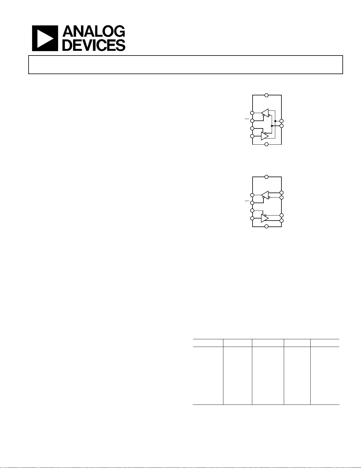
FUNCTIONAL BLOCK DIAGRAMS
CC
ADN4691E/
ADN4696E
RO R
RE
DE
D
DI
GND
Figure 1.
V
CC
ADN4693E/
ADN4697E
RO R
RE
DE
D
DI
GND
Figure 2.
A
B
10355-001
A
B
Z
Y
10355-002
APPLICATIONS
Backplane and cable multipoint data transmission
Multipoint clock distribution
Low power, high speed alternative to shorter RS-485 links
Networking and wireless base station infrastructure
GENERAL DESCRIPTION
The ADN4691E/ADN4693E/ADN4696E/ADN4697E are
multipoint, low voltage differential signaling (M-LVDS)
transceivers (driver and receiver pairs) that can operate at up to
200 Mbps (100 MHz). The receivers detect the bus state with a
differential input of as little as 50 mV over a common-mode
voltage range of −1 V to +3.4 V. ESD protection of up to ±15 kV
is implemented on the bus pins. The parts adhere to the
TIA/EIA-899 standard for M-LVDS and complement TIA/EIA644 LVDS devices with additional multipoint capabilities.
The ADN4691E/ADN4693E are Type 1 receivers with 25 mV of
hysteresis, so that slow-changing signals or loss of input does
not lead to output oscillations. The ADN4696E/ADN4697E are
Type 2 receivers exhibiting an offset threshold, guaranteeing the
output state when the bus is idle (bus-idle fail-safe) or the inputs are
open (open-circuit fail-safe).
A
Rev.
Information furnished by Analog Devices is believed to be accurate and reliable. However, no
responsibility is assumed by Anal og Devices for its use, nor for any infringements of patents or ot her
rights of third parties that may result from its use. Specifications subject to change without notice. No
license is granted by implication or otherwise under any patent or patent rights of Analog Devices.
Trademarks and registered trademarks are the property of their respective owners.
The parts are available as half-duplex in an 8-lead SOIC package
(the ADN4691E/ADN4696E) or as full-duplex in a 14-lead
SOIC package (the ADN4693E/ADN4697E). A selection table
for the ADN469xE parts is shown in Ta ble 1.
Table 1. ADN469xE Selection Table
Part No. Receiver Data Rate SOIC Duplex
ADN4690E Type 1 100 Mbps 8-lead Half
ADN4691E Type 1 200 Mbps 8-lead Half
ADN4692E Type 1 100 Mbps 14-lead Full
ADN4693E Type 1 200 Mbps 14-lead Full
ADN4694E Type 2 100 Mbps 8-lead Half
ADN4695E Type 2 100 Mbps 14-lead Full
ADN4696E Type 2 200 Mbps 8-lead Half
ADN4697E Type 2 200 Mbps 14-lead Full
One Technology Way, P.O. Box 9106, Norwood, MA 02062-9106, U.S.A.
Tel: 781.329.4700 www.analog.com
Fax: 781.461.3113 ©2011–2012 Analog Devices, Inc. All rights reserved.
Page 2

ADN4691E/ADN4693E/ADN4696E/ADN4697E Data Sheet
TABLE OF CONTENTS
Features.............................................................................................. 1
Applications....................................................................................... 1
Functional Block Diagrams............................................................. 1
General Description ......................................................................... 1
Revision History ........................................................................... 2
Specifications..................................................................................... 3
Receiver Input Threshold Test Voltages.................................... 4
Timing Specifications .................................................................. 5
Absolute Maximum Ratings............................................................ 6
Thermal Resistance ...................................................................... 6
ESD Caution.................................................................................. 6
Pin Configurations and Function Descriptions ........................... 7
Typical Performance Characteristics ............................................. 8
Test Circuits and Switching Characteristics................................ 11
Driver Voltage and Current Measurements............................ 11
Driver Timing Measurements .................................................. 12
Receiver Timing Measurements............................................... 13
Theory of Operation ...................................................................... 14
Half-Duplex/Full-Duplex Operation....................................... 14
Three-State Bus Connection..................................................... 14
Truth Tables................................................................................. 14
Glitch-Free Power-Up/Power-Down....................................... 15
Fault Conditions......................................................................... 15
Receiver Input Thresholds/Fail-Safe........................................ 15
Applications Information.............................................................. 16
Outline Dimensions....................................................................... 17
Ordering Guide .......................................................................... 17
REVISION HISTORY
3/12—Rev. 0 to Rev. A
Added ADN4691E and ADN4693E................................. Universal
Changes to Features Section, General Description Section,
and Table 1..........................................................................................1
Added Type 1 Receiver Parameters, Table 2 ..................................3
Added Table 3, Renumbered Sequentially .....................................4
Added Type 1 Receiver Parameters, Table 5 ..................................5
Added Table 7.....................................................................................6
Changes to Table 8............................................................................. 7
Changes to Figure 33.......................................................................13
Added Table 12 ................................................................................14
Changes to Receiver Input Thresholds/Fail-Safe Section
and Figure 36....................................................................................15
Changes to Ordering Guide........................................................... 17
12/11—Revision 0: Initial Version
Rev. A | Page 2 of 20
Page 3

Data Sheet ADN4691E/ADN4693E/ADN4696E/ADN4697E
SPECIFICATIONS
VCC = 3.0 V to 3.6 V; RL = 50 ; TA = T
Table 2.
Parameter Symbol Min Typ Max Unit Test Conditions/Comments
DRIVER
Differential Outputs
Differential Output Voltage Magnitude |VOD| 480 650 mV See Figure 19
∆|VOD| for Complementary Output States ∆|VOD| −50 +50 mV See Figure 19
Common-Mode Output Voltage (Steady State) V
ΔV
for Complementary Output States ΔV
OC(SS)
Peak-to-Peak VOC V
Maximum Steady-State Open-Circuit Output
Voltage
Voltage Overshoot
Low to High VPH 1.2VSS V See Figure 24, Figure 27
High to Low VPL −0.2VSS V See Figure 24, Figure 27
Output Current
Short Circuit |IOS| 24 mA See Figure 22
High Impedance State, Driver Only IOZ −15 +10 μA
Power Off I
Output Capacitance CY or CZ 3 pF
Differential Output Capacitance CYZ 2.5 pF VAB = 0.4 sin(30e6πt) V,2 DE = 0 V
Output Capacitance Balance (CY/CZ) C
Logic Inputs (DI, DE)
Input High Voltage VIH 2 VCC V
Input Low Voltage VIL GND 0.8 V
Input High Current IIH 0 10 μA VIH = 2 V
Input Low Current IIL 0 10 μA VIL = 0.8 V
RECEIVER
Differential Inputs
Differential Input Threshold Voltage
Type 1 Receiver (ADN4691E, ADN4693E) VTH −50 +50 mV See Table 3, Figure 36
Type 2 Receiver (ADN4696E, ADN4697E) VTH 50 150 mV See Table 4 , Figure 36
Input Hysteresis
Type 1 Receiver (ADN4691E, ADN4693E) V
Type 2 Receiver (ADN4696E, ADN4697E) V
Differential Input Voltage Magnitude |VID| 0.05 VCC V
Input Capacitance CA or CB 3 pF
Differential Input Capacitance CAB 2.5 pF VAB = 0.4 sin(30e6πt) V2
Input Capacitance Balance (CA/CB) C
Logic Output RO
Output High Voltage VOH 2.4 V IOH = –8 mA
Output Low Voltage VOL 0.4 V IOL = 8 mA
High Impedance Output Current IOZ −10 +15 μA VO = 0 V or 3.6 V
Logic Input RE
Input High Voltage VIH 2 VCC V
Input Low Voltage VIL GND 0.8 V
Input High Current IIH −10 0 μA VIH = 2 V
Input Low Current IIL −10 0 μA VIL = 0.8 V
MIN
to T
, unless otherwise noted. 1
MAX
0.8 1.2 V See Figure 20, Figure 23
OC(SS)
−50 +50 mV See Figure 20, Figure 23
OC(SS)
150 mV See Figure 20, Figure 23
OC(PP)
V
, V
,
A(O)
B(O)
, or V
V
Y(O)
O(OFF)
Y/Z
HYS
HYS
A/B
Z(O)
−10 +10 μA
0.99 1.01
25 mV
0 mV
0.99 1.01
0 2.4 V See Figure 21
–1.4 V ≤ (V
or VZ) ≤ 3.8 V,
Y
other output = 1.2 V
–1.4 V ≤ (V
or VZ) ≤ 3.8 V,
Y
other output = 1.2 V, 0 V ≤ V
= 0.4 sin(30e6πt) V + 0.5 V,2
V
I
other output = 1.2 V, DE = 0 V
= 0.4 sin(30e6πt) V + 0.5 V,2
V
I
other input = 1.2 V
≤ 1.5 V
CC
Rev. A | Page 3 of 20
Page 4
ADN4691E/ADN4693E/ADN4696E/ADN4697E Data Sheet
Parameter Symbol Min Typ Max Unit Test Conditions/Comments
BUS INPUT/OUTPUT
Input Current
A (Receiver or Transceiver with Driver Disabled) IA 0 32 μA VB = 1.2 V, VA = 3.8 V
−20 +20 μA VB = 1.2 V, VA = 0 V or 2.4 V
−32 0 μA VB = 1.2 V, VA = −1.4 V
B (Receiver or Transceiver with Driver Disabled) IB 0 32 μA VA = 1.2 V, VB = 3.8 V
−20 +20 μA VA = 1.2 V, VB = 0 V or 2.4 V
−32 0 μA VA = 1.2 V, VB = −1.4 V
−4 +4 μA VA = VB, 1.4 V ≤ VA ≤ 3.8 V
Differential (Receiver or Transceiver with Driver
Disabled)
Power-Off Input Current 0 V ≤ VCC ≤ 1.5 V
A (Receiver or Transceiver) I
−20 +20 μA VB = 1.2 V, VA = 0 V or 2.4 V
−32 0 μA VB = 1.2 V, VA = −1.4 V
B (Receiver or Transceiver) I
−20 +20 μA VA = 1.2 V, VB = 0 V or 2.4 V
−32 0 μA VA = 1.2 V, VB = −1.4 V
Differential (Receiver or Transceiver) I
Input Capacitance (Transceiver with Driver Disabled) CA or CB 5 pF
Differential Input Capacitance (Transceiver with
Driver Disabled)
Input Capacitance Balance (CA/CB) (Transceiver
with Driver Disabled)
POWER SUPPLY
Supply Current ICC
Only Driver Enabled 13 22 mA
Both Driver and Receiver Disabled 1 4 mA
Both Driver and Receiver Enabled 16 24 mA
Only Receiver Enabled 4 13 mA
1
All typical values are given for VCC = 3.3 V and TA = 25°C.
2
HP4194A impedance analyzer (or equivalent).
I
AB
0 32 μA VB = 1.2 V, VA = 3.8 V
A(OFF)
0 32 μA VA = 1.2 V, VB = 3.8 V
B(OFF)
−4 +4 μA VA = VB, 1.4 ≤ VA ≤ 3.8 V
AB(OFF)
= 0.4 sin(30e6πt) V + 0.5 V,2
V
I
other input = 1.2 V, DE = 0 V
3 pF VAB = 0.4 sin(30e6πt) V,2 DE = 0 V
C
AB
C
0.99 1.01 DE = 0 V
A/B
= VCC, RL = 50 Ω
DE, RE
DE = 0 V, RE
DE = V
DE, RE
= VCC, RL = no load
, RE = 0 V, RL = 50 Ω
CC
= 0 V, RL = 50 Ω
RECEIVER INPUT THRESHOLD TEST VOLTAGES
RE
= 0 V, H = high, L = low
Table 3. Test Voltages for Type 1 Receiver
Applied Voltages Input Voltage, Differential Input Voltage, Common Mode Receiver Output
VA (V) VB (V) VID (V) VIC (V) RO (V)
2.4 0 2.4 1.2 H
0 2.4 −2.4 1.2 L
3.8 3.75 0.05 3.775 H
3.75 3.8 −0.05 3.775 L
−1.35 −1.4 0.05 −1.375 H
−1.4 −1.35 −0.05 −1.375 L
Rev. A | Page 4 of 20
Page 5

Data Sheet ADN4691E/ADN4693E/ADN4696E/ADN4697E
Table 4. Test Voltages for Type 2 Receiver
Applied Voltages Input Voltage, Differential Input Voltage, Common Mode Receiver Output
VA (V) VB (V) VID (V) VIC (V) RO (V)
+2.4 0 +2.4 +1.2 H
0 +2.4 −2.4 +1.2 L
+3.8 +3.65 +0.15 +3.725 H
+3.8 +3.75 +0.05 +3.775 L
−1.25 −1.4 +0.15 −1.325 H
−1.35 −1.4 +0.05 −1.375 L
TIMING SPECIFICATIONS
VCC = 3.0 V to 3.6 V; TA = T
Table 5.
Parameter Symbol Min Typ Max Unit Test Conditions/Comments
DRIVER
Maximum Data Rate 200 Mbps
Propagation Delay t
Differential Output Rise/Fall Time tR, tF 1 1.6 ns See Figure 24, Figure 27
Pulse Skew |t
PHL
– t
PLH
Part-to-Part Skew2 t
Period Jitter, RMS (1 Standard Deviation)3 t
Peak-to-Peak Jitter
3, 5
Disable Time from High Level t
Disable Time from Low Level t
Enable Time to High Level t
Enable Time to Low Level t
RECEIVER
Propagation Delay t
Rise/Fall Time tR, tF 1 2.3 ns CL = 15 pF (see Figure 30, Figure 33)
Pulse Skew |t
RPHL
– t
RPLH
Type 1 Receiver (ADN4691E,
ADN4693E)
Type 2 Receiver (ADN4696E,
ADN4697E)
Part-to-Part Skew2 t
Period Jitter, RMS (1 Standard Deviation)3 t
Peak-to-Peak Jitter
3, 5
Type 1 Receiver (ADN4691E,
ADN4693E)
Type 2 Receiver (ADN4696E,
ADN4697E)
Disable Time from High Level t
Disable Time from Low Level t
Enable Time to High Level t
Enable Time to Low Level t
1
All typical values are given for VCC = 3.3 V and TA = 25°C.
2
t
is defined as the difference between the propagation delays of two devices between any specified terminals. This specification applies to devices at the same VCC
SK(PP)
and temperature, and with identical packages and test circuits.
3
Jitter parameters are guaranteed by design and characterization. Values do not include stimulus jitter.
4
tR = tF = 0.5 ns (10% to 90%), measured over 30,000 samples.
5
Peak-to-peak jitter specifications include jitter due to pulse skew (tSK).
6
tR = tF = 0.5 ns (10% to 90%), measured over 100,000 samples.
7
|VID| = 400 mV (ADN4696E, ADN4697E), Vic = 1.1 V, tR = tF = 0.5 ns (10% to 90%), measured over 30,000 samples.
8
|VID| = 400 mV (ADN4696E, ADN4697E), Vic = 1.1 V, tR = tF = 0.5 ns (10% to 90%), measured over 100,000 samples.
to T
MIN
, unless otherwise noted.1
MAX
, t
1 1.5 2.4 ns See Figure 24, Figure 27
PLH
PHL
| tSK 0 100 ps See Figure 24, Figure 27
1 ns See Figure 24, Figure 27
SK(PP)
2 3 ps 100 MHz clock input4 (see Figure 26)
J(PER)
t
| tSK C
30 130 ps 200 Mbps 215 − 1 PRBS input6 (see Figure 29)
J(PP)
7 ns See Figure 25, Figure 28
PHZ
7 ns See Figure 25, Figure 28
PLZ
7 ns See Figure 25, Figure 28
PZH
7 ns See Figure 25, Figure 28
PZL
, t
RPLH
2 4 6 ns CL = 15 pF (see Figure 30, Figure 33)
RPHL
= 15 pF (see Figure 30, Figure 33)
L
100 300 ps
300 500 ps
1 ns CL = 15 pF (see Figure 30, Figure 33)
SK(PP)
4 7 ps 100 MHz clock input7 (see Figure 32)
J(PER)
t
200 Mbps 215 − 1 PRBS input8 (see Figure 35)
J(PP)
t
300 700 ps
J(PP)
450 800 ps
10 ns See Figure 31, Figure 34
RPHZ
10 ns See Figure 31, Figure 34
RPLZ
15 ns See Figure 31, Figure 34
RPZH
15 ns See Figure 31, Figure 34
RPZL
Rev. A | Page 5 of 20
Page 6
ADN4691E/ADN4693E/ADN4696E/ADN4697E Data Sheet
ABSOLUTE MAXIMUM RATINGS
= T
MIN
to T
T
A
, unless otherwise noted.
MAX
Table 6.
Parameter Rating
VCC −0.5 V to +4 V
Digital Input Voltage (DE, RE, DI)
Receiver Input (A, B) Voltage
Half-Duplex (ADN4691E, ADN4696E) −1.8 V to +4 V
Full-Duplex (ADN4693E, ADN4697E) −4 V to +6 V
Receiver Output Voltage (RO) −0.3 V to +4 V
Driver Output (A, B, Y, Z) Voltage −1.8 V to +4 V
ESD Rating (A, B, Y, Z Pins)
HBM (Human Body Model)
Air Discharge ±15 kV
Contact Discharge ±8 kV
IEC 61000-4-2, Air Discharge ±10 kV
IEC 61000-4-2, Contact Discharge ±8 kV
ESD Rating (Other Pins, HBM) ±4 kV
ESD Rating (All Pins)
FICDM ±1.25 kV
Machine Model ±400 V
Operating Temperature Range −40°C to +85°C
Storage Temperature Range −65°C to +150°C
−0.5 V to +4 V
THERMAL RESISTANCE
θJA is specified for the worst-case conditions, that is, a device
soldered in a circuit board for surface-mount packages.
Table 7. Thermal Resistance
Package Type θJA Unit
8-Lead SOIC 121 °C/W
14-Lead SOIC 86 °C/W
ESD CAUTION
Stresses above those listed under Absolute Maximum Ratings
may cause permanent damage to the device. This is a stress
rating only; functional operation of the device at these or any
other conditions above those indicated in the operational
section of this specification is not implied. Exposure to absolute
maximum rating conditions for extended periods may affect
device reliability.
Rev. A | Page 6 of 20
Page 7

Data Sheet ADN4691E/ADN4693E/ADN4696E/ADN4697E
PIN CONFIGURATIONS AND FUNCTION DESCRIPTIONS
14
13
12
11
9
8
RO
RE
DE
DI
1
ADN4691E/
2
ADN4696E
3
TOP VIEW
(Not to Scale)
4
V
8
CC
7
B
A
6
GND
5
10355-003
Figure 3. ADN4691E/ADN4696E Pin Configuration
NC
1
2
RO
ADN4693E/
3
RE
ADN4697E
TOP VIEW
4
DE
(Not to Scal e)
5 10
DI
6
GND
GND
7
NC = NO CONNE CT
Figure 4. ADN4693E/ADN4697E Pin Configuration
Table 8. Pin Function Descriptions
ADN4691E/
ADN4696E
Pin No.
ADN4693E/
ADN4697E
Pin No. Mnemonic Description
1 2 RO Receiver Output. Type 1 receiver (ADN4691E/ADN4693E), when enabled:
If A − B ≥ 50 mV, then RO = logic high. If A − B ≤ −50 mV, then RO = logic low.
Type 2 receiver (ADN4696E/ADN4697E), when enabled:
If A − B ≥ 150 mV, then RO = logic high. If A − B ≤ 50 mV, then RO = logic low.
Receiver output is undefined outside these conditions.
2 3
Receiver Output Enable. A logic low on this pin enables the receiver output, RO.
RE
A logic high on this pin places RO in a high impedance state.
3 4 DE
Driver Output Enable. A logic high on this pin enables the driver differential outputs.
A logic low on this pin places the driver differential outputs in a high impedance state.
4 5 DI Driver Input. Half-duplex (ADN4691E/ADN4696E), when enabled:
A logic low on DI forces A low and B high, whereas a logic high on DI forces A high and B low.
Full-duplex (ADN4693E/ADN4697E), when enabled:
A logic low on DI forces Y low and Z high, whereas a logic high on DI forces Y high and Z low.
5 6, 7 GND
N/A 9 Y
N/A 10 Z
6 N/A A
N/A 12 A
7 N/A B
N/A 11 B
8 13, 14 V
Power Supply (3.3 V ± 0.3 V).
CC
Ground.
Noninverting Driver Output Y.
Inverting Driver Output Z.
Noninverting Receiver Input A and Noninverting Driver Output A.
Noninverting Receiver Input A.
Inverting Receiver Input B and Inverting Driver Output B.
Inverting Receiver Input B.
N/A 1, 8 NC No Connect. Do not connect to these pins.
V
V
A
B
Z
Y
NC
CC
CC
10355-004
Rev. A | Page 7 of 20
Page 8

ADN4691E/ADN4693E/ADN4696E/ADN4697E Data Sheet
A
T
TYPICAL PERFORMANCE CHARACTERISTICS
20
18
16
DRIVER
14
(mA)
CC
12
10
8
6
SUPPLY CURRENT, I
(mA)
SUPPLY CURRENT, I
RECEIVER (V
4
2
0
0 20406080100120
Figure 5. Power Supply Current (I
= 3.3 V, TA = 25°C; Receiver VID = 250 mV, VIC = 1 V)
(V
CC
20
18
DRIVER
16
14
CC
12
10
RECEIVER (V
8
6
4
2
0
–50 –30 –10 10 30 50 70 90
= 250mV, VIC = 1V)
ID
FREQUENC Y (MHz)
= 250mV, VIC = 1V)
ID
TEMPERATURE (°C)
) vs. Frequency
CC
Figure 6. Power Supply Current vs. Temperature (Data Rate = 200 Mbps,
V
= 3.3 V; Receiver VID = 250 mV, VIC = 1 V)
CC
40
(mA)
OL
35
30
25
20
15
10
VCC=3V
VCC=3.3V
VCC=3.6V
5
10355-005
10355-006
0
VCC = 3.0V
–5
–10
–15
–20
–25
–30
–35
–40
–45
RECEIVER HIG H LEVEL OUT PUT CURRENT (mA)
–50
VCC = 3.3V
VCC = 3.6V
0 0.5 1.0 1.5 2.0 2.5 3.0 3.5 4.0
RECEIVER HIGH LEVEL OUTPUT VOLTAGE, VOH (V)
Figure 8. Receiver Output Current vs. Output Voltage (Output High)
= 25°C)
(T
A
2.0
1.8
(V)
OD
1.6
1.4
AGE, V
1.2
1.0
0.8
L OUTPUT VOL
0.6
0.4
0.2
DIFFERENTI
0
02468101214
OUTPUT CURRENT, IO (mA)
Figure 9. Driver Differential Output Voltage vs. Output Current
= 3.3 V, TA = 25°C)
(V
CC
2.4
t
PHL
t
PLH
2.2
2.0
1.8
1.6
1.4
DRIVER PROPAG ATION DEL AY (ns)
1.2
10355-008
10355-009
0
RECEIVER LOW LEVEL OUTPUT CURREN T, I
0 0.5 1.0 1.5 2.0 2.5 3.0 3.5 4.0
RECEIVER LO W LEVEL OUTPUT VOLTAGE, VOL (V)
10355-007
Figure 7. Receiver Output Current vs. Output Voltage (Output Low)
= 25°C)
(T
A
Rev. A | Page 8 of 20
1.0
–40 –20 0 20 40 60 80
TEMPERATURE, TA (°C)
Figure 10. Driver Propagation Delay vs. Temperature
(Data Rate = 2 Mbps, V
= 3.3 V)
CC
10355-010
Page 9

Data Sheet ADN4691E/ADN4693E/ADN4696E/ADN4697E
G
A
A
6.0
t
5.5
Y (ns)
5.0
4.5
TION DEL
4.0
3.5
3.0
RECEIVER PROPA
2.5
2.0
RPLH
t
RPHL
–50 –30 –10 10 30 50 70 90
TEMPERATURE, TA (°C)
Figure 11. Receiver Propagation Delay vs. Temperature
(Data Rate = 2 Mbps, V
3.0
2.5
2.0
1.5
1.0
0.5
ADDED DRIVER PERIOD JI TTER (ps)
= 3.3 V, VID = 400 mV, VIC = 1.1 V)
CC
10355-011
120
100
80
60
40
20
ADDED DRIVER PEAK-TO-PEAK JITTER (ps)
0
–50 –30 –10 10 30 50 70 90
TEMPERATURE, TA (°C)
Figure 14. Driver Jitter (Peak-to-Peak) vs. Temperature
(Data Rate = 200 Mbps, V
7
6
5
4
3
2
1
ADDED RECEIVER P ERIOD JI TTER (ps)
= 3.3 V, PRBS 215 − 1 Input)
CC
10355-014
0
20 30 40 50 60 70 80 90 100
FREQUE NCY (MHz )
Figure 12. Driver Jitter (Period) vs. Frequency
= 3.3 V, TA = 25°C, Clock Input)
(V
CC
120
100
80
60
40
20
ADDED DRIVER PEAK- TO-PEAK JITTER (ps)
0
0 20 40 60 80 100 120 140 160 180 200
DATA RATE (Mbps)
Figure 13. Driver Jitter (Peak-to-Peak) vs. Data Rate
= 3.3 V, TA = 25°C, PRBS 215 − 1 Input)
(V
CC
0
0 20406080100120
10355-012
FREQUENCY (MHz)
10355-015
Figure 15. Receiver Jitter (Period) vs. Frequency
= 3.3 V, TA = 25°C, VID = 400 mV)
(V
CC
800
700
600
500
400
300
200
100
ADDED RECEIVER P EAK– TO–PEAK JIT TER (ps)
0
–50 –30 –10 10 30 50 70 90
10355-013
TEMPERATURE ( °C)
10355-016
Figure 16. Receiver Jitter (Peak-to-Peak) vs. Temperature
(Data Rate = 200 Mbps, V
= 3.3 V, VID = 400 mV, VIC = 1.1 V,
CC
15
− 1 Input)
PRBS 2
Rev. A | Page 9 of 20
Page 10

ADN4691E/ADN4693E/ADN4696E/ADN4697E Data Sheet
V
V
200mV/DI
1ns/DIV
Figure 17. ADN4696E Driver Output Eye Pattern
(Data Rate = 200 Mbps, PRBS 2
15
− 1 Input, RL = 50 Ω)
10355-017
500mV/DI
2.5ns/DI V
Figure 18. ADN4696E Receiver Output Eye Pattern
(Data Rate = 200 Mbps, PRBS 2
15
− 1 Input, CL = 15 pF)
10355-018
Rev. A | Page 10 of 20
Page 11

Data Sheet ADN4691E/ADN4693E/ADN4696E/ADN4697E
V
V
V
A/Y
TEST CIRCUITS AND SWITCHING CHARACTERISTICS
DRIVER VOLTAGE AND CURRENT MEASUREMENTS
A/Y
49.9Ω
B/Z
V
OD
DI
NOTES
1. 1% TOLERANCE FOR ALL RESI STORS
3.32kΩ
3.32kΩ
V
+
TEST
–
–1V TO +3.4V
Figure 19. Driver Voltage Measurement over Common-Mode Range
24.9Ω
24.9Ω
R1
R2
C3
V
OC
2.5pF
10355-020
A/Y
DI
B/Z
NOTES
1. C1, C2, AND C3 ARE 20% AND INCL UDE PROBE/ STRAY
CAPACITANCE LESS THAN 2cm FROM DU T.
2. R1 AND R2 ARE 1%, METAL FILM, SURFACE MOUNT,
LESS THAN 2cm FROM DUT.
C1
1pF
C2
1pF
Figure 20. Driver Common-Mode Output Voltage Measurement
CC
A/Y
S1 S2
Z(O)
R1
,
1.62kΩ
±1%
V
B/ZDE
, V
A(O)
B(O)
OR V
V
Y(O)
I
A/Y
B/Z
OS
S2
V
TEST
–1V OR +3. 4V
10355-022
V
CC
DI
S1
10355-019
Figure 22. Driver Short Circuit
≈ 1.3V
B/Z
V
OC
NOTES
1. INPUT PULSE GENERATOR: 500kHz; 50% ± 5% DUTY CYCLE; t
MEASURED ON TEST EQUIPMENT WITH –3dB BANDWIDTH ≥ 1GHz.
2.
OC(PP)
OC(PP)
∆V
OC(SS)
, tF ≤ 1ns.
R
≈ 0.7V
10355-023
Figure 23. Driver Common-Mode Output Voltage (Steady State)
10355-021
Figure 21. Maximum Steady-State Output Voltage Measurement
Rev. A | Page 11 of 20
Page 12

ADN4691E/ADN4693E/ADN4696E/ADN4697E Data Sheet
V
V
(
V
V
V
DRIVER TIMING MEASUREMENTS
A/Y
DI
B/Z
NOTES
1. C1, C2, AND C3 ARE 20% AND INCL UDE PROBE/ STRAY
CAPACITANCE LESS THAN 2cm FROM DU T.
2. R1 IS 1%, METAL FILM, SURFACE MOUNT,
LESS THAN 2cm FROM DUT.
C1
1pF
C2
1pF
C3
0.5pF
OUT
R1
50Ω
Figure 24. Driver Timing Measurement
CC
A/Y
DI
S1
DE
B/Z
NOTES
1. C1, C2, C3, AND C4 ARE 20% AND I NCLUDE PRO BE/ST RAY
CAPACITANCE LESS THAN 2cm FROM DUT.
2. R1 AND R2 ARE 1%, METAL FILM, SURFACE MOUNT,
LESS THAN 2cm FROM DUT.
C1
1pF
C2
1pF
C4
0.5pF
OUT
R1
24.9Ω
R2
24.9Ω
Figure 25. Driver Enable/Disable Time
CC
INPUT
(CLOCK)
0V
/2 VCC/2
V
CC
1/f0
C3
2.5pF
10355-024
10355-025
CC
t
0.5V
PHL
CC
90% V
t
F
SS
10% V
V
PH
SS
0% V
0V
V
OUT
DI
SS
0.5V
CC
t
PLH
90% V
SS
0V 0V
10% V
SS
SS
t
R
NOTES
t
,
t
1. INPUT PULSE GENE RATOR: 500kHz; 50% ± 5% DUT Y CYCLE;
2. MEASURED O N TEST EQUIPM ENT WITH –3dB BANDW IDTH ≥ 1GHz.
≤ 1ns.
R
F
Figure 27. Driver Propagation, Rise/Fall Times and Voltage Overshoot
DE
0.5V
CC
t
PZL
OUT
(DI = 0V)
OUT
)
(DI = V
CC
NOTES
1. INPUT PUL SE GENERATOR: 500kHz; 50% ± 5% DUT Y CYCLE;
2. MEASURED ON T EST EQ UIPMENT W ITH –3dB BANDW IDTH ≥ 1GHz.
–0.1V
t
PZH
0.1V
0.5V
t
PLZ
t
PHZ
CC
–0.1V
0.1V
t
,
t
≤ 1ns.
R
F
Figure 28. Driver Enable/Disable Times
V
PL
CC
0V
0V
~ –0.6V
~ 0.6V
0V
10355-027
10355-028
OUTPUT
– V
V
A
OR
– V
V
Y
(IDEAL)
B
Z
0V 0V
1/f0
OUTPUT
– V
V
A
B
OR
– V
V
Y
Z
ACTUAL )
NOTES
1. INPUT PULSE GENERATOR: AGILENT 8304A STIMULUS SYSTEM;
100MHz; 50% ± 1% DUTY CYCL E.
2. MEASURED USI NG TEK T DS6604 WITH T DSJIT3 SO FTWARE.
0V 0V
t
c(n)
t
= |
t
c(n)
– 1/f0|
J(PER)
Figure 26. Driver Period Jitter Characteristics
(PRBS)
V
V
OUTPUT
VA – V
V
NOTES
1. INPUT P ULSE GENERATOR: AGILENT 8304A STI MULUS SYS TEM;
200Mbps; 2
10355-026
2. MEASURED USI NG TEK TDS6604 WITH T DSJIT3 SOF TWARE.
Rev. A | Page 12 of 20
INPUT
– V
A
OR
– V
Y
OR
– V
Y
CC
0.5V
CC
0V
B
Z
0V 0V
B
Z
15
– 1PRBS.
t
J(PP)
Figure 29. Driver Peak-to-Peak Jitter Characteristics
0.5V
CC
10355-029
Page 13

Data Sheet ADN4691E/ADN4693E/ADN4696E/ADN4697E
A
V
V
V
V
V
RECEIVER TIMING MEASUREMENTS
V
ID
NOTES
IS 20%, CERAMI C, SURFACE MOUN T, AND INCLUDES
1. C
L
PROBE/ST RAY CAPACITANCE < 2cm FROM DUT.
RO
RE
B
C
L
V
15pF
OUT
Figure 30. Receiver Timing Measurement
1.4
1.0V
1.2V
RE INPUT
NOTES
IS 20% AND INCLUDES PROBE/STRAY
1. C
L
CAPACITANCE < 2cm FROM DUT.
IS 1% METAL FILM, SURFACE MOUNT, <2cm FROM DUT.
2. R
L
A
RO
B
RE
C
L
15pF
R
L
499Ω
V
V
OUT
TEST
Figure 31. Receiver Enable/Disable Time
INPUT
– VB)
(V
A
0V
1/f0
V
OH
OUTPUT
(IDEAL)
V
OL
0.5V
CC
1/f0
V
OH
OUTPUT
(ACTUAL)
V
OL
NOTES
1. INPUT PULSE GENERATOR: AGILENT 8304A STIMULUS SYSTEM;
100MHz; 50% ± 1% DUTY CYCLE.
2. MEASURED USING TEK TDS6604 WITH TDSJIT3 SOFTWARE.
0.5V
CC
t
c(n)
t
= |
t
c(n)
– 1f0|
J(PER)
Figure 32. Receiver Period Jitter Characteristics
0.5V
0.5V
A
V
B
10355-030
V
ID
V
OH
OUT
V
OL
NOTES
1. INPUT PULSE GENERATOR: 50MHz; 50% ± 5% DUT Y CYCLE; t
10355-031
2. MEASURED ON T EST EQUI PMENT WI TH –3dB BANDWIDT H ≥ 1GHz.
0V
t
90%
RPHL
0.5V
CC
10%
t
F
0V
t
0.5V
10%
RPLH
90%
CC
t
R
, tF ≤ 1ns.
R
10355-033
Figure 33. Receiver Propagation and Rise/Fall Times
CC
RE INPUT
V
OUT
= VCC)
(V
TEST
(A = 1V)
CC
V
OUT
(V
= 0V)
TEST
(A = 1.4V)
NOTES
1. INPUT PULSE GENERATOR: 500kHz; 50% ± 5% DUT Y CYCLE;
CC
A
INPUT
(PRBS)
V
B
10355-032
V
OH
0.5V
t
RPZL
t
RPZH
CC
0.5V
CC
0.5V
CC
t
RPLZ
t
RPHZ
0.5V
CC
Figure 34. Receiver Enable/Disable Times
VOL + 0.5V
VOH – 0.5V
t
,
t
R
F
≤ 1ns.
0V
V
CC
V
OL
V
OH
0V
10355-034
OUTPUT
V
OL
NOTES
1. INPUT PULSE GENERATOR: AGILENT 8304A STIMULUS SYSTEM;
200Mbps; 2
2. MEASURED USING TEK T DS6604 WITH TDSJIT 3 SOFTWARE.
15
– 1PRBS.
0.5V
t
J(PP)
CC
0.5V
CC
10355-035
Figure 35. Receiver Peak-to-Peak Jitter Characteristics
Rev. A | Page 13 of 20
Page 14

ADN4691E/ADN4693E/ADN4696E/ADN4697E Data Sheet
THEORY OF OPERATION
The ADN4691E/ADN4693E/ADN4696E/ADN4697E are
transceivers for transmitting and receiving multipoint, low
voltage differential signaling (M-LVDS) at high speed (data
rates up to 200 Mbps). Each device has a differential line driver
and a differential line receiver, allowing each device to send and
receive data.
Multipoint LVDS expands on the established LVDS low voltage
differential signaling method by allowing bidirectional communication between more than two nodes. Up to 32 nodes can be
connected on an M-LVDS bus.
HALF-DUPLEX/FULL-DUPLEX OPERATION
Half-duplex operation allows a transceiver to transmit or
receive, but not both at the same time. However, with fullduplex operation, a transceiver can transmit and receive
simultaneously. The ADN4691E/ADN4696E are half-duplex
devices in which the driver and the receiver share differential
bus terminals. The ADN4693E/ADN4697E are full-duplex
devices that have dedicated driver output and receiver input
pins. Figure 37 and Figure 38 show typical half- and full-duplex
bus topologies, respectively, for M-LVDS.
THREE-STATE BUS CONNECTION
The outputs of the device can be placed in a high impedance
state by disabling the driver or receiver. This allows several
driver outputs to be connected to a single M-LVDS bus. Note
that, on each bus line, only one driver can be enabled at a time,
but many receivers can be enabled at the same time.
The driver can be enabled or disabled using the driver enable
pin (DE). DE enables the driver outputs when taken high; when
taken low, DE puts the driver outputs into a high impedance state.
Similarly, an active low receiver enable pin (
receiver. Taking
RE
low enables the receiver, whereas taking it
high puts the receiver outputs into a high impedance state.
Truth tables for driver and receiver output states under various
conditions are shown in Tab l e 1 0 , Tab l e 1 1 , Tab l e 1 2 and
Tabl e 13 .
RE
) controls the
Driver, Half Duplex (ADN4691E/ADN4696E)
Table 10. Transmitting (See Table 9 for Abbreviations)
Inputs Outputs
Power
Yes H H H L
Yes H L L H
Yes H NC L H
Yes L X Z Z
Yes NC X Z Z
≤1.5 V X X Z Z
DE DI A B
Driver, Full Duplex (ADN4693E/ADN4697E)
Table 11. Transmitting (See Table 9 for Abbreviations)
Inputs Outputs
Power
Yes H H H L
Yes H L L H
Yes H NC L H
Yes L X Z Z
Yes NC X Z Z
≤1.5 V X X Z Z
DE DI Y Z
Type 1 Receiver (ADN4691E/ADN4693E)
Table 12. Receiving (see Table 9 for Abbreviations)
Inputs Output
Power
Yes ≥50 mV L H
Yes ≤−50 mV L L
Yes −50 mV < A − B < 50 mV L I
Yes N C L I
Yes X H Z
Yes X NC Z
No X X Z
A − B
RO
RE
Type 2 Receiver (ADN4696E/ADN4697E)
TRUTH TABLES
Table 9. Truth Table Abbreviations
Abbreviation Description
H High level
L Low level
X Don’t care
I Indeterminate
Z High impedance (off )
NC Disconnected
Table 13. Receiving (See Table 9 for Abbreviations)
Power
Yes ≥150 mV L H
Yes ≤50 mV L L
Yes 50 mV < A − B < 150 mV L I
Yes N C L L
Yes X H Z
Yes X NC Z
No X X Z
Rev. A | Page 14 of 20
A − B
Inputs Output
RE
RO
Page 15

Data Sheet ADN4691E/ADN4693E/ADN4696E/ADN4697E
R
A
V
R
GLITCH-FREE POWER-UP/POWER-DOWN
To minimize disruption to the bus when adding nodes, the
M-LVDS outputs of the device are kept glitch-free when the
device is powering up or down. This feature allows insertion of
devices onto a live M-LVDS bus because the bus outputs are not
switched on before the device is fully powered. In addition, all
outputs are placed in a high impedance state when the device is
powered off.
FAULT CONDITIONS
The ADN4691E/ADN4693E/ADN4696E/ADN4697E contain
short-circuit current protection that protects the part under
fault conditions in the case of short circuits on the bus. This
protection limits the current in a fault condition to 24 mA at
the transmitter outputs for short-circuit faults between −1 V
and +3.4 V. Any network fault must be cleared to avoid data
transmission errors and to ensure reliable operation of the data
network and any devices that are connected to the network.
RECEIVER INPUT THRESHOLDS/FAIL-SAFE
Two receiver types are available, both of which incorporate
protection against short circuits.
The Type 1 receivers of the ADN4691E/ADN4693E incorporate
25 mV of hysteresis. This ensures that slow-changing signals or
a loss of input does not result in oscillation of the receiver output.
Type 1 receiver thresholds are ±50 mV; therefore, the state of the
receiver output is indeterminate if the differential between A and
B is about 0 V. This state occurs if the bus is idle (approximately 0 V
on both A and B), with no drivers enabled on the attached nodes.
Type 2 receivers (ADN4696E/ADN4697E) have an open circuit
and bus-idle fail-safe. The input threshold is offset by 100 mV so
that a logic low is present on the receiver output when the bus is
idle or when the receiver inputs are open.
The different receiver thresholds for the two receiver types are
illustrated in Figure 36. See Ta ble 12 and Ta b le 1 3 for receiver
output states under various conditions.
TYPE 1 RECEIVE
OUTPUT
) [V]
IB
–
L INPUT VOLTAGE (V
DIFFERENTI
0.25
IA
0.15
0.05
–0.05
–0.15
LOGIC 1
0
UNDEFINED
LOGIC 0
Figure 36. Input Threshold Voltages
TYPE 2 RECEIVE
OUTPUT
LOGIC 1
UNDEFINED
LOGIC 0
10355-036
Rev. A | Page 15 of 20
Page 16

ADN4691E/ADN4693E/ADN4696E/ADN4697E Data Sheet
APPLICATIONS INFORMATION
M-LVDS extends the low power, high speed, differential
signaling of LVDS (low voltage differential signaling) to
multipoint systems where multiple nodes are connected over
short distances in a bus topology network.
With M-LVDS, a transmitting node drives a differential signal
across a transmission medium such as a twisted pair cable. The
transmitted differential signal allows other receiving nodes that
are connected along the bus to detect a differential voltage that
can then be converted back into a single-ended logic signal by
the receiver.
The communication line is typically terminated at both ends
by resistors (R
), the value of which is chosen to match the
T
characteristic impedance of the medium (typically 100 Ω).
For half-duplex multipoint applications such as the one shown
in Figure 37, only one driver can be enabled at any time. Fullduplex nodes allow a master-slave topology as shown in Figure 38.
In this configuration, a master node can concurrently send and
receive data to/from slave nodes. At any time, only one slave
node can have its driver enabled to concurrently transmit data
back to the master node.
R
T
AB
AB
ADN4696E
R
R
RO
NOTES
1. MAXIMUM NUMBER OF NO DES: 32.
IS EQUAL TO THE CHARACT ERISTI C IMPEDANCE OF THE CABLE USED.
2. R
T
D
D
RE
DE DI RO RE
Figure 37. ADN4696E Typical Half-Duplex M-LVDS Network (Type 2 Receivers with Threshold Offset for Bus-Idle Fail-Safe)
R
T
R
T
ADN4696E
R
R
D
D
DE DI RO RE
AB
R
R
AB
ADN4696E
R
D
D
DE DI RO RE
R
ADN4696E
D
D
DE DI
R
T
10355-037
R
T
R
T
ABZY
MASTER SLAVE SLAVE SLAVE
ADN4697E
R
RO
NOTES
1. MAXIMUM NUMBER OF NO DES: 32.
IS EQUAL TO THE CHARACT ERISTI C IMPEDANCE OF THE CABLE USED.
2. R
T
D
RE
DE DI RO RE DE DI RO RE DE DI
ABZY
ADN4697E
R
Figure 38. ADN4697E Typical Full-Duplex M-LVDS Master-Slave Network (Type 2 Receivers with Threshold Offset for Bus-Idle Fail-Safe)
D
Rev. A | Page 16 of 20
ABZY
R
ADN4697E
D
ABZY
ADN4697E
R
RO RE DE DI
D
10355-038
Page 17

Data Sheet ADN4691E/ADN4693E/ADN4696E/ADN4697E
OUTLINE DIMENSIONS
5.00 (0.1968)
4.80 (0.1890)
4.00 (0.1574)
3.80 (0.1497)
0.25 (0.0098)
0.10 (0.0040)
COPLANARITY
0.10
CONTROLLING DIMENSIONS ARE IN MILLIMETERS; INCH DIMENSIONS
(IN PARENTHESES) ARE ROUNDED-OFF MILLIMETER EQUIVALENTS FOR
REFERENCE ONLY AND ARE NOT APPROPRIATE FOR USE IN DESIGN.
85
1
1.27 (0.0500)
SEATING
PLANE
COMPLIANT TO JEDEC STANDARDS MS-012-AA
BSC
6.20 (0.2441)
5.80 (0.2284)
4
1.75 (0.0688)
1.35 (0.0532)
0.51 (0.0201)
0.31 (0.0122)
8°
0°
0.25 (0.0098)
0.17 (0.0067)
0.50 (0.0196)
0.25 (0.0099)
1.27 (0.0500)
0.40 (0.0157)
45°
012407-A
Figure 39. 8-Lead Standard Small Outline Package [SOIC_N]
Narrow Body
(R-8)
Dimensions shown in millimeters and (inches)
8.75 (0.3445)
8.55 (0.3366)
BSC
8
6.20 (0.2441)
5.80 (0.2283)
7
1.75 (0.0689)
1.35 (0.0531)
SEATING
PLANE
8°
0°
0.25 (0.0098)
0.17 (0.0067)
0.50 (0.0197)
0.25 (0.0098)
1.27 (0.0500)
0.40 (0.0157)
45°
4.00 (0.1575)
3.80 (0.1496)
0.25 (0.0098)
0.10 (0.0039)
COPLANARIT Y
0.10
14
1
1.27 (0.0500)
0.51 (0.0201)
0.31 (0.0122)
CONTROLL ING DIMENSIONS ARE IN MIL LIMET ERS; INCH DIMENSIONS
(IN PARENTHESES) ARE ROUNDED-OFF MILL IMETE R EQUIVALENTS FOR
REFERENCE ON LY AND ARE NOT APPROPRIATE FOR USE I N DESIGN.
COMPLIANT TO JEDEC STANDARDS MS-012-AB
060606-A
Figure 40. 14-Lead Standard Small Outline Package [SOIC_N]
Narrow Body
(R-14)
Dimensions shown in millimeters and (inches)
ORDERING GUIDE
Model1 Temperature Range Package Description Package Option
ADN4691EBRZ –40°C to +85°C 8-Lead Standard Small Outline Package (SOIC_N) R-8
ADN4691EBRZ-RL7 –40°C to +85°C 8-Lead Standard Small Outline Package (SOIC_N) R-8
ADN4693EBRZ –40°C to +85°C 14-Lead Standard Small Outline Package (SOIC_N) R-14
ADN4693EBRZ-RL7 –40°C to +85°C 14-Lead Standard Small Outline Package (SOIC_N) R-14
ADN4696EBRZ –40°C to +85°C 8-Lead Standard Small Outline Package (SOIC_N) R-8
ADN4696EBRZ-RL7 –40°C to +85°C 8-Lead Standard Small Outline Package (SOIC_N) R-8
ADN4697EBRZ –40°C to +85°C 14-Lead Standard Small Outline Package (SOIC_N) R-14
ADN4697EBRZ-RL7 –40°C to +85°C 14-Lead Standard Small Outline Package (SOIC_N) R-14
EVAL-ADN469xEHDEBZ Evaluation Board for Half-Duplex (ADN4691E/ADN4696E)
EVAL-ADN469xEFDEBZ Evaluation Board for Full-Duplex (ADN4693E/ADN4697E)
1
Z = RoHS Compliant Part.
Rev. A | Page 17 of 20
Page 18

ADN4691E/ADN4693E/ADN4696E/ADN4697E Data Sheet
NOTES
Rev. A | Page 18 of 20
Page 19

Data Sheet ADN4691E/ADN4693E/ADN4696E/ADN4697E
NOTES
Rev. A | Page 19 of 20
Page 20

ADN4691E/ADN4693E/ADN4696E/ADN4697E Data Sheet
NOTES
©2011–2012 Analog Devices, Inc. All rights reserved. Trademarks and
registered trademarks are the property of their respective owners.
D10355-0-3/12(A)
Rev. A | Page 20 of 20
 Loading...