

3 V, LVDS, Quad CMOS
FEATURES
±8 kV ESD IEC 61000-4-2 contact discharge on receiver input pins
400 Mbps (200 MHz) switching rates
100 ps channel-to-channel skew (typical)
100 ps differential skew (typical)
3.3 ns propagation delay (maximum)
3.3 V power supply
High impedance outputs on power-down
Low power design (10 mW quiescent typical)
Interoperable with existing 5 V LVDS drivers
Accepts small swing (350 mV typical) differential
input signal levels
Supports open, short, and terminated input fail-safe
Conforms to TIA/EIA-644 LVDS standard
Industrial operating temperature range of −40°C to +85°C
Available in surface-mount SOIC package and low profile
TSSOP package
APPLICATIONS
Point-to-point data transmission
Multidrop buses
Clock distribution networks
Backplane receivers
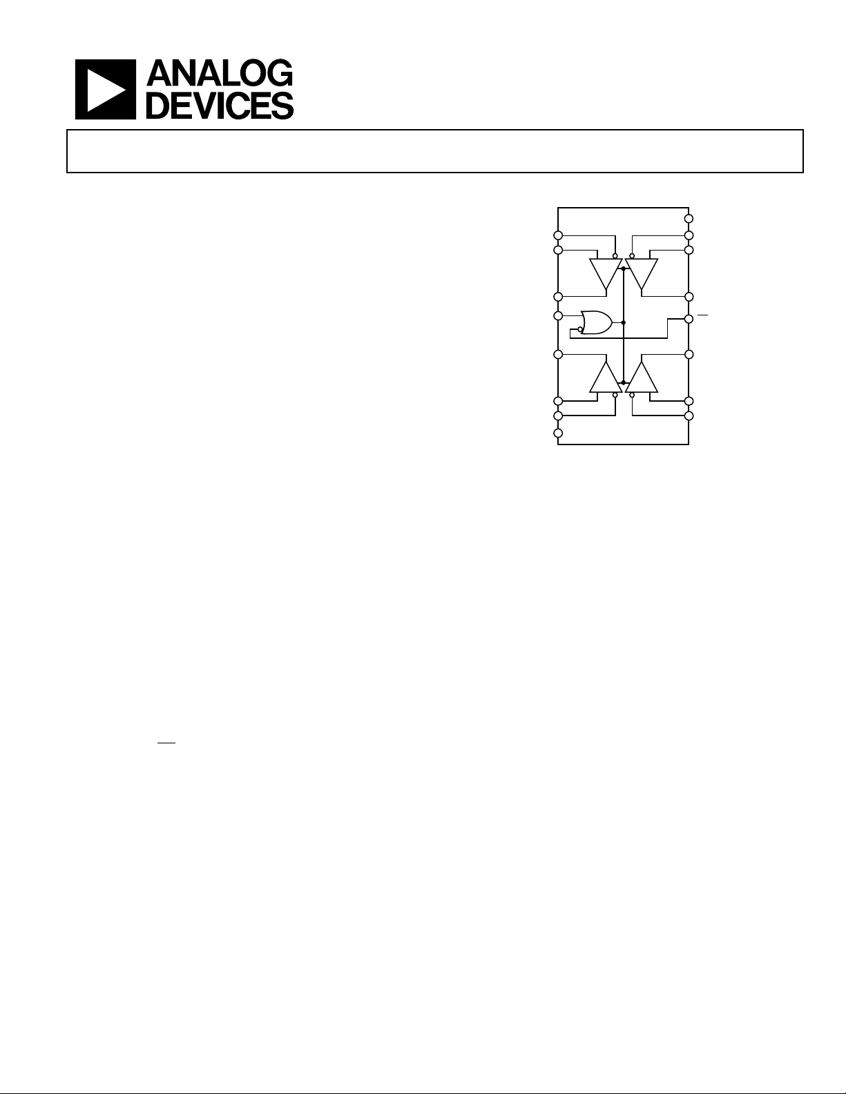
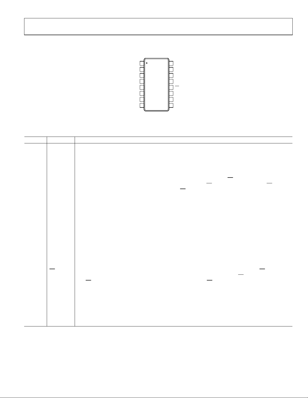
Differential Line Receiver
ADN4666
FUNCTIONAL BLOCK DIAGRAM
V
R
R
R
EN
R
R
R
CC
IN4–
IN4+
OUT4
OUT3
IN3+
IN3–
08097-001
ADN4666
R
IN1–
R
IN1+
R4
R1
R
OUT1
EN
R
OUT2
R3
R2
R
IN2+
R
IN2–
GND
Figure 1.
GENERAL DESCRIPTION
The ADN4666 is a quad-channel, CMOS low voltage differential
signaling (LVDS) line receiver offering data rates of over 400 Mbps
(200 MHz) and ultralow power consumption.
The device accepts low voltage (350 mV typical) differential
input signals and converts them to a single-ended, 3 V TTL/CMOS
logic level.
The ADN4666 also offers active high and active low enable/disable
inputs (EN and
Rev. 0
Information furnished by Analog Devices is believed to be accurate and reliable. However, no
responsibility is assumed by Analog Devices for its use, nor for any infringements of patents or other
rights of third parties that may result from its use. Specifications subject to change without notice. No
license is granted by implication or otherwise under any patent or patent rights of Analog Devices.
Trademarks and registered trademarks are the property of their respective owners.
EN
) that control all four receivers. These inputs
disable the receivers and switch the outputs to a high impedance
state. Consequently, the outputs of one or more ADN4666
devices can be multiplexed together to reduce the quiescent
power consumption to 10 mW typical.
The ADN4666 and its companion driver, the ADN4665, offer
a new solution to high speed, point-to-point data transmission
and offer a low power alternative to emitter-coupled logic (ECL)
or positive emitter-coupled logic (PECL).
One Technology Way, P.O. Box 9106, Norwood, MA 02062-9106, U.S.A.
Tel: 781.329.4700 www.analog.com
Fax: 781.461.3113 ©2009 Analog Devices, Inc. All rights reserved.

ADN4666
TABLE OF CONTENTS
Features .............................................................................................. 1
Applications ....................................................................................... 1
Functional Block Diagram .............................................................. 1
General Description ......................................................................... 1
Revision History ............................................................................... 2
Specifications ..................................................................................... 3
Timing Specifications .................................................................. 4
Absolute Maximum Ratings ............................................................ 6
REVISION HISTORY
6/09—Revision 0: Initial Version
ESD Caution...................................................................................6
Pin Configuration and Function Descriptions ..............................7
Typical Performance Characteristics ..............................................8
Theory of Operation .........................................................................9
Enable Inputs .................................................................................9
Applications Information .............................................................9
Outline Dimensions ....................................................................... 10
Ordering Guide .......................................................................... 10
Rev. 0 | Page 2 of 12
ADN4666
SPECIFICATIONS
VCC = 3.0 V to 3.6 V, CL = 15 pF to GND, all specifications T
MIN
to T
, unless otherwise noted.
MAX
Table 1.
Parameter Symbol Min Typ Max Unit Test Conditions/Comments
LVDS INPUTS (R
Differential Input High Threshold at R
Differential Input Low Threshold at R
Common-Mode Voltage Range at R
Input Current at R
INx+
, R
INx−
INx+
)
, R
INx+
, R
INx+
, R
INx+
INx−
, R
IIN −10 ±5 +10 μA VIN = 2.8 V, VCC = 3.6 V or 0 V
INx−
3
VTH 20 100 mV VCM = 1.2 V, 0.05 V, 2.95 V
INx−
3
V
INx−
4
−100 −20 mV VCM = 1.2 V, 0.05 V, 2.95 V
TL
V
0.1 2.3 V VID = 200 mV p-p
CMR
−10 ±1 +10 μA VIN = 0 V, VCC = 3.6 V or 0 V
−20 ±1 +20 μA VIN = 3.6 V, VCC = 0 V
Input High Voltage VIH 2.0 VCC V
Input Low Voltage VIL GND 0.8 V
Input Current IIN −10 ±1 +10 μA VIN = 0 V or VCC, other input = VCC or GND
Input Clamp Voltage VCL −1.5 −0.8 V ICL = −18 mA
OUTPUTS (R
)
OUTx
Output High Voltage VOH 2.7 3.0 V IOH = −0.4 mA, VID = 200 mV
2.7 3.0 V IOH = −0.4 mA, input terminated
2.7 3.0 V IOH = −0.4 mA, input shorted
Output Low Voltage VOL 0.1 0.25 V IOL = 2 mA, VID = −200 mV
Output Short-Circuit Current
5
IOS −15 −48 −120 mA Outputs enabled, V
Output Off State Current IOZ −10 ±1 +10 μA Outputs disabled, V
POWER SUPPLY
No Load Supply, Current Receivers Enabled ICC 10 15 mA
No Load Supply, Current Receivers Disabled I
3 5 mA
CCZ
ESD PROTECTION
R
, R
INx+
Pins ±8 kV IEC 61000-4-2 contact discharge
INx−
±15 kV Human body model
All Pins Except R
1
Current into device pins is defined as positive. Current out of device pins is defined as negative. All voltages are referenced to ground, unless otherwise specified.
2
All typical values are given for VCC = 3.3 V and TA = 25°C.
3
VCC is always higher than the R
common-mode voltage range is 0.1 V to 2.3 V.
4
V
is reduced for larger input differential voltage (VID). For example, if VID is 400 mV, V
CMR
over the common-mode range of 0 V to 2.4 V, but is supported only with inputs shorted and no external common-mode voltage applied. VID up to VCC − 0 V can be
applied to the R
400 mV. Skew specifications apply for 200 mV ≤ VID ≤ 800 mV over the common-mode range.
5
Output short-circuit current (IOS) is specified as magnitude only; a minus sign indicates direction only. Note that only one output should be shorted at a time; do not
exceed the maximum junction temperature specification (150°C).
, R
INx+
INx+/RINx−
±4 kV Human body model
INx−
and R
INx+
inputs with the common-mode voltage set to VCC/2. Propagation delay and differential pulse skew decrease when VID is increased from 200 mV to
voltage. R
INx−
INx−
and R
have a voltage range of −0.2 V to VCC − VID/2. However, to be compliant with ac specifications, the
INx+
is 0.2 V to 2.2 V. The fail-safe condition with inputs shorted is not supported
CMR
1, 2
EN and EN
EN = GND and EN
= 0 V
OUT
= 0 V or VCC
OUT
= VCC or GND, inputs open
= VCC, inputs open
Rev. 0 | Page 3 of 12
ADN4666
V
TIMING SPECIFICATIONS
VCC = 3.0 V to 3.6 V, CL = 15 pF to GND, all specifications T
MIN
to T
, unless otherwise noted.1
MAX
Table 2.
Parameter
2
Symbol Min Typ3Max Unit Test Conditions/Comments
4, 5
AC CHARACTERISTICS
Differential Propagation Delay, High to Low t
Differential Propagation Delay, Low to High t
Differential Pulse Skew6 |t
Differential Channel-to-Channel Skew
(Same Device)
7
Differential Part-to-Part Skew
Differential Part-to-Part Skew
PHLD
− t
8
9
| t
PLHD
Rise Time t
Fall Time t
Disable Time, High to Z t
Disable Time, Low to Z t
Enable Time, Z to High t
Enable Time, Z to Low t
Maximum Operating Frequency
1
Generator waveform for all tests, unless otherwise specified: f = 1 MHz, ZO = 50 Ω, t
2
AC parameters are guaranteed by design and characterization.
3
All typical values are given for VCC = 3.3 V and TA = 25°C.
4
Current into device pins is defined as positive. Current out of device pins is defined as negative. All voltages are referenced to ground, unless otherwise specified.
5
CL includes load and jig capacitance.
6
t
is the magnitude difference in the differential propagation delay time between the positive-going edge and the negative-going edge of the same channel.
SKD1
7
Channel-to-channel skew, t
the inputs.
8
t
part-to-part skew is the differential channel-to-channel skew of any event between devices. The t
SKD3
5°C of each other within the operating temperature range.
9
t
part-to-part skew is the differential channel-to-channel skew of any event between devices. The t
SKD4
operating temperature and voltage ranges and across process distribution. t
10
f
generator input conditions: f = 200 MHz, t
MAX
duty cycle, VOL (maximum = 0.4 V), VOH (minimum = 2.7 V), and load = 15 pF (stray plus probes).
SKD2
10
, is defined as the difference between the propagation delay of one channel and that of the others on the same chip with any event on
= t
TLH
THL
1.8 3.3 ns CL = 15 pF, VID = 300 mV (see Figure 2 and Figure 3)
PHLD
1.8 3.3 ns CL = 15 pF, VID = 300 mV (see Figure 2 and Figure 3)
PLHD
0 0.1 0.35 ns CL = 15 pF, VID = 300 mV (see Figure 2 and Figure 3)
SKD1
t
0 0.1 0.5 ns CL = 15 pF, VID = 300 mV (see Figure 2 and Figure 3)
SKD2
t
1.0 ns CL = 15 pF, VID = 300 mV (see Figure 2 and Figure 3)
SKD3
t
1.5 ns CL = 15 pF, VID = 300 mV (see Figure 2 and Figure 3)
SKD4
0.35 1.2 ns CL = 15 pF, VID = 300 mV (see Figure 2 and Figure 3)
TLH
0.35 1.2 ns CL = 15 pF, VID = 300 mV (see Figure 2 and Figure 3)
THL
8 12 ns RL = 2 kΩ, CL = 15 pF (see Figure 4 and Figure 5)
PHZ
8 12 ns RL = 2 kΩ, CL = 15 pF (see Figure 4 and Figure 5)
PLZ
11 17 ns RL = 2 kΩ, CL = 15 pF (see Figure 4 and Figure 5)
PZH
11 17 ns RL = 2 kΩ, CL = 15 pF (see Figure 4 and Figure 5)
PZL
f
200 250 MHz All channels switching
MAX
and t
TLH
is defined as |maximum − minimum| differential propagation delay.
SKD4
(0% to 100%) ≤ 3 ns for R
THL
specification applies to devices at the same VCC and within
SKD3
specification applies to devices over the recommended
SKD4
< 1 ns (0% to 100%), 50% duty cycle, differential (1.05 V to 1.35 V p-p). f
INx+/RINx−
.
generator output criteria: 60%/40%
MAX
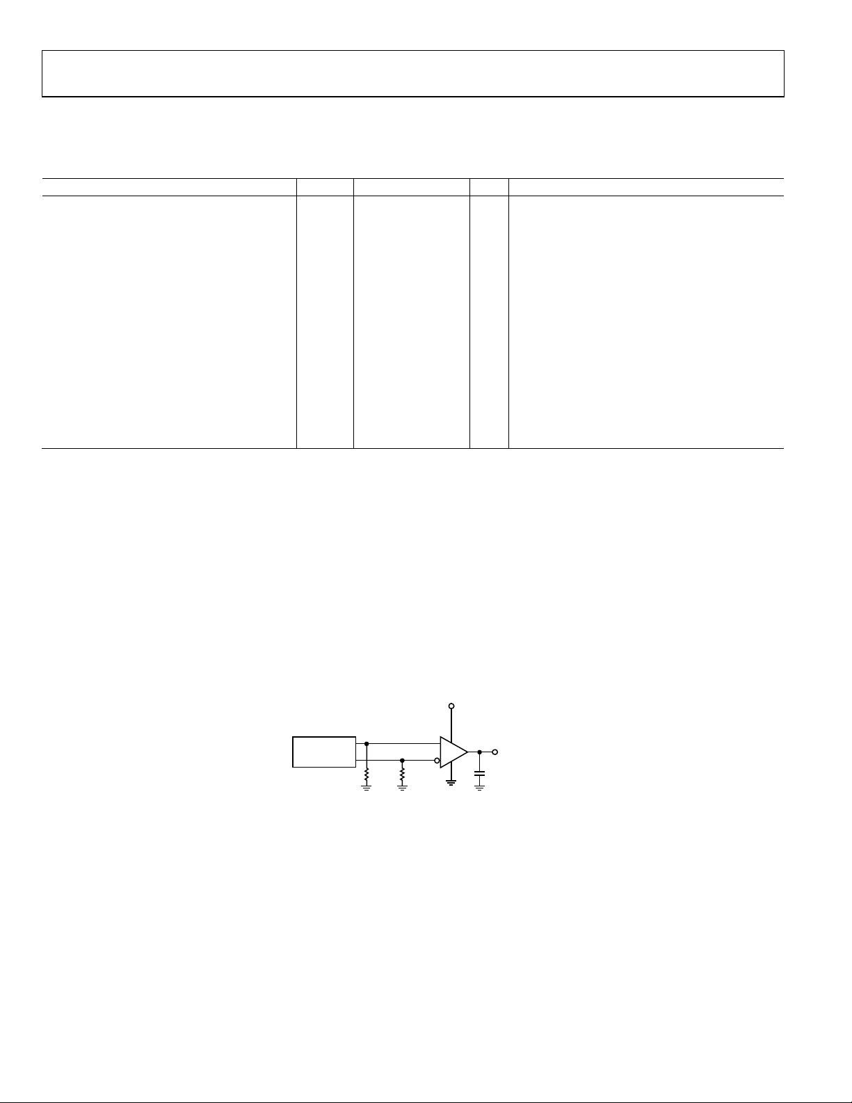
Test Circuits and Timing Diagrams
CC
R
SIGNAL
GENERATOR
50Ω 50Ω
NOTES
= LOAD AND TEST JIG CAPACITANCE.
1. C
L
INx+
R
INx–
RECEIVER
IS ENABLED
R
OUTx
C
L
08097-002
Figure 2. Test Circuit for Receiver Propagation Delay and Transition Time
Rev. 0 | Page 4 of 12
ADN4666
V
V
R
R
R
OUTx
INx–
INx+
0V (DIFFERENTIAL)
t
PLHD
1.5V
20%
t
TLH
VID= 300mV p-p
1.2V
t
PHLD
80%80%
t
THL
1.5V
20%
1.3V
1.1V
V
OH
V
OL
08097-003
Figure 3. Receiver Propagation Delay and Transition Time Waveforms
CC
R
INx+
R
INx–
EN
SIGNAL
GENERATOR
NOTES
INCLUDES LOAD AND TEST JIG CAPACITANCE.
1. C
L
2. S1 CONNECTED TO V
3. S1 CO NNECT E D TO GND FOR
50Ω
EN
GND
FOR
t
AND
t
CC
PZL
t
PZH
AND
PLZ
t
PHZ
MEASUREMENTS.
MEASUREMENTS.
Figure 4. Test Circuit for Receiver Enable/Disable Delay
S1
R
L
R
OUTx
C
L
08097-004
EN WITH EN = GND
OR OPEN CI RCUI T
1.5V
1.5V
3
0V
3V
EN WITH EN = V
R
WITH VID = +100mV
OUTx
WITH VID = –100mV
R
OUTx
1.5V
CC
t
t
PHZ
PLZ
0.5V
0.5V
1.5V
t
PZH
t
PZL
50%
50%
0V
V
OH
GND
V
CC
V
OL
08097-005
Figure 5. Receiver Enable/Disable Delay Waveforms
Rev. 0 | Page 5 of 12
ADN4666
ABSOLUTE MAXIMUM RATINGS
TA = 25°C, unless otherwise noted.
Table 3.
Parameter Rating
VCC to GND −0.3 V to +4 V
Input Voltage (R
Enable Input Voltage (EN, EN) to GND
Output Voltage (R
Industrial Operating Temperature Range −40°C to +85°C
Storage Temperature Range −65°C to +150°C
Maximum Junction Temperature (T
θJA Thermal Impedance 150.4°C/W
Power Dissipation (T
Reflow Soldering Peak Temperature,
Pb-Free
, R
INx+
) to GND −0.3 V to VCC + 0.3 V
INx−
−0.3 V to V
) to GND −0.3 V to VCC + 0.3 V
OUTx
) 150°C
J MAX
− TA)/θJA
J MAX
260°C ± 5°C
+ 0.3 V
CC
Stresses above those listed under Absolute Maximum Ratings
may cause permanent damage to the device. This is a stress
rating only; functional operation of the device at these or any
other conditions above those indicated in the operational
section of this specification is not implied. Exposure to absolute
maximum rating conditions for extended periods may affect
device reliability.
ESD CAUTION
Rev. 0 | Page 6 of 12
ADN4666
PIN CONFIGURATION AND FUNCTION DESCRIPTIONS
16
V
CC
15
R
IN4–
14
R
IN4+
R
13
OUT4
12
EN
R
11
OUT3
10
R
IN3+
9
R
IN3–
08097-006
R
R
R
R
OUT1
OUT2
R
R
GND
IN1–
IN1+
EN
IN2+
IN2–
1
2
3
ADN4666
TOP VIEW
4
(Not to Scale)
5
6
7
8
Figure 6. Pin Configuration
Table 4. Pin Function Descriptions
Pin No. Mnemonic Description
1 R
2 R
3 R
IN1−
IN1+
OUT1
Receiver Channel 1 Inverting Input. When this input is more negative than R
, R
more positive than R
IN1+
OUT1
is low.
Receiver Channel 1 Noninverting Input. When this input is more positive than R
, R
is more negative than R
IN1−
OUT1
is low.
Receiver Channel 1 Output (3 V TTL/CMOS). If the differential input voltage between R
output is high. If the differential input voltage is negative, this output is low.
4 EN
5 R
OUT2
Active High Enable and Power-Down Input (3 V TTL/CMOS). When EN is low and EN is high, the receiver outputs
are disabled and are in a high impedance state. When EN is high and
EN
the receiver outputs are enabled. When EN is high and
is high, the receiver outputs are enabled.
EN
Receiver Channel 2 Output (3 V TTL/CMOS). If the differential input voltage between R
output is high. If the differential input voltage is negative, this output is low.
6 R
7 R
IN2+
IN2−
Receiver Channel 2 Noninverting Input. When this input is more positive than R
, R
is more negative than R
IN2−
OUT2
is low.
Receiver Channel 2 Inverting Input. When this input is more negative than R
more positive than R
IN2+
, R
OUT2
is low.
8 GND Ground Reference Point for All Circuitry on the Part.
9 R
10 R
11 R
IN3−
IN3+
OUT3
Receiver Channel 3 Inverting Input. When this input is more negative than R
, R
more positive than R
IN3+
OUT3
is low.
Receiver Channel 3 Noninverting Input. When this input is more positive than R
, R
is more negative than R
IN3−
OUT3
is low.
Receiver Channel 3 Output (3 V TTL/CMOS). If the differential input voltage between R
output is high. If the differential input voltage is negative, this output is low.
12
EN
Active Low Enable and Power-Down Input with Pull-Down (3 V TTL/CMOS). ). When EN is low and EN is high, the
receiver outputs are disabled and are in a high impedance state. When EN is high and
EN
is low, the receiver outputs are enabled. When EN is high and EN is high, the receiver outputs are enabled.
and
13 R
OUT4
Receiver Channel 4 Output (3 V TTL/CMOS). If the differential input voltage between R
output is high. If the differential input voltage is negative, this output is low.
14 R
15 R
IN4+
IN4−
Receiver Channel 4 Noninverting Input. When this input is more positive than R
, R
is more negative than R
IN4−
OUT4
is low.
Receiver Channel 4 Inverting Input. When this input is more negative than R
, R
more positive than R
IN4+
OUT4
is low.
16 VCC Power Supply Input. The ADN4666 can be operated from 3.0 V to 3.6 V.
, R
IN1+
is high. When this input is
OUT1
, R
IN1−
is high. When this input
OUT1
IN1+
and R
is positive, this
IN1−
is low or when EN is low and EN is low,
IN2+
IN3+
IN4+
and R
IN2+
, R
IN2−
, R
, R
IN3−
IN4−
, R
is high. When this input
OUT2
is high. When this input is
OUT2
is high. When this input is
OUT3
, R
is high. When this input
OUT3
and R
IN3+
EN
is low or when EN is low
and R
IN4+
, R
is high. When this input
OUT4
is high. When this input is
OUT4
is positive, this
IN2−
is positive, this
IN3−
is positive, this
IN4−
Rev. 0 | Page 7 of 12
ADN4666
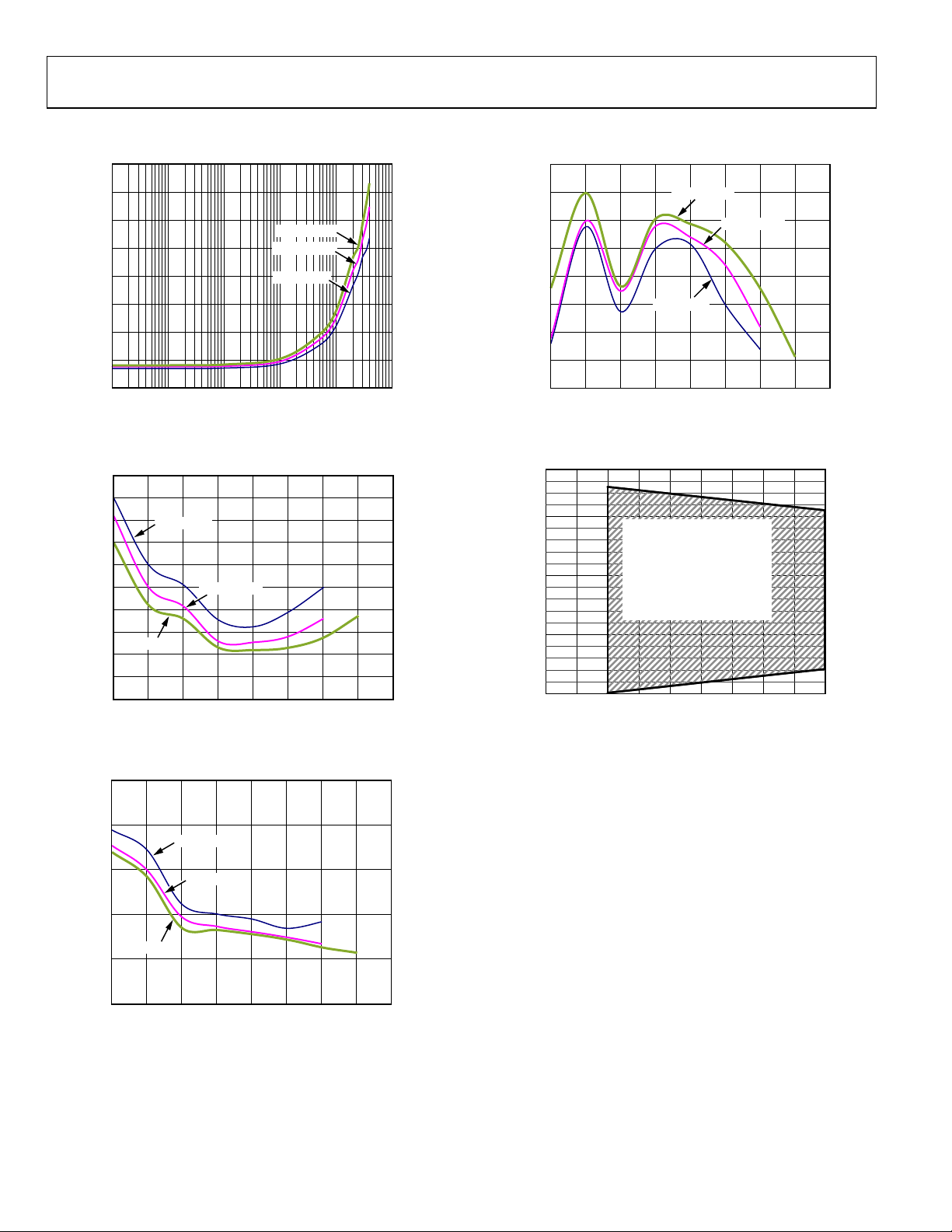
TYPICAL PERFORMANCE CHARACTERISTICS
80
200
70
60
50
40
30
20
POWER SUPPLY CURRENT (mA)
10
0
0.01 0.1 1 10 100 1k
FREQUENCY (MHz )
3.6V SUPPLY
3.3V SUPPL Y
3V SUPPLY
Figure 7. Power Supply Current vs. Frequency
2.9
2.8
2.7
2.6
2.5
2.4
2.3
2.2
2.1
2.0
DIFFERENTIAL PROP AGATION DELAY (ns)
1.9
–0.1 0.4 0.9 1.4 1.9 2.4 2.9 3.4 3.9
Figure 8. Differential Propagation Delay (t
2.9
3V SUPPLY
3.6V SUPPLY
3.3V SUPPLY
COMMON-MODE VOLTAGE (V)
) vs. Common-Mode Voltage, 25°C
PLHD
150
100
50
0
SKEW (ps)
–50
–100
–150
–200
–0.1 0.4 0.9 1.4 1.9 2.4 2.9 3.4 3.9
08097-007
COMMON-MODE VOLTAGE (V)
3.6V SUPPL Y
3.3V SUPPLY
3V SUPPLY
08097-010
Figure 10. Skew vs. Common-Mode Voltage, 25°C
3
(V)
IN
2
COMMON-MODE V
1
0
–0.1 0 0.1 0.2 0.3 0.4 0.5 0.6 0.7 0.8
08097-008
VCC = 3.3V
T
= 25°C
A
f
= 100MHz
IN
2 CHANNELS SWI TCHING
MAX PROP DELAY MEASURED,
t
, t
PLHD
PLHD
–
V
ID
t
PHLD
(V)
= 2.54ns
| = 280ps
PHLD
MAX SKEW MEASURED
|
t
08097-011
Figure 11. Typical Common-Mode Range Variation
with Respect to the Amplitude of the Differential Input
2.7
3V SUPPLY
2.5
2.3
3.6V SUPPLY
2.1
DIFFERENTIAL PROPAGATION DELAY (ns)
1.9
–0.1 0.4 0.9 1.4 1.9 2.4 2.9 3.4 3.9
3.3V SUPPLY
COMMON-MODE VOLTAGE ( V)
Figure 9. Differential Propagation Delay (t
) vs. Common-Mode Voltage, 25°C
PHLD
08097-009
Rev. 0 | Page 8 of 12

ADN4666
THEORY OF OPERATION
The ADN4666 is a quad-channel line receiver for low voltage
differential signaling (LVDS). It takes a differential input signal
of 350 mV typical and converts it into a single-ended, 3 V TTL/
CMOS logic signal.
A differential current input signal, received via a transmission
medium such as a twisted pair cable, develops a voltage across
a termination resistor, R
. This resistor is chosen to match the
T
characteristic impedance of the medium, typically around 100 Ω.
The differential voltage is detected by the receiver and converted
back into a single-ended logic signal.
When the noninverting receiver input, R
to the inverting input, R
R
from R
T
receiver input, R
input, R
to R
INx+
to R
INx+
INx−
INx+
(that is, when current flows through RT from R
INx−
), R
is low.
OUTx
(that is, when current flows through
INx−
), R
is high. When the noninverting
OUTx
, is negative with respect to the inverting
, is positive with respect
INx+
INx−
Using the ADN4665 as a driver, the received differential current
is between ±2.5 mA and ±4.5 mA (±3.5 mA typical), developing
between ±250 mV and ±450 mV across a 100 Ω termination
resistor. The received voltage is centered around the receiver
offset of 1.2 V. Therefore, the noninverting receiver input is
typically 1.375 V (that is, 1.2 V + [350 mV/2]) and the inverting
receiver input is 1.025 V (that is, 1.2 V − [350 mV/2]) for a
Logic 1. For a Logic 0, the inverting and noninverting input
voltages are reversed. Note that because the differential voltage
reverses polarity, the peak-to-peak voltage swing across R
is
T
twice the differential voltage.
Current-mode drivers offer considerable advantages over voltagemode drivers, such as the RS-422 drivers. The operating current
remains fairly constant with increased switching frequency,
whereas the operating current of voltage-mode drivers increases
exponentially in most cases. This increase is caused by the overlap
as internal gates switch between high and low, causing currents
to flow from V
to ground. A current-mode device reverses a
CC
constant current between its two outputs, with no significant
overlap currents.
This is similar to emitter-coupled logic (ECL) and positive emittercoupled logic (PECL), but without the high quiescent current of
ECL and PECL.
ENABLE INPUTS
The ADN4666 has active high and active low enable inputs that
put all the logic outputs into a high impedance state when disabled,
reducing device current consumption from 10 mA typical to 3 mA
typical. See Tab l e 5 for a truth table of the enable inputs.
Table 5. Enable Inputs Truth Table
Pin Logic Level
EN
EN
Low High X
R
R
INx+
1
X
INx−
1
High-Z
R
OUTx
Low Low 1.025 V 1.375 V 0
Low Low 1.375 V 1.025 V
High Low 1.025 V 1.375 V
1
0
High Low 1.375 V 1.025 V 1
1
X = don’t care.
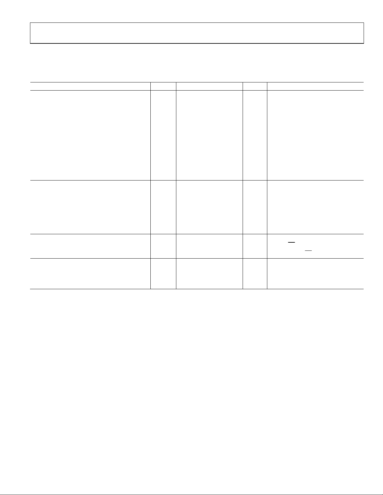
APPLICATIONS INFORMATION
Figure 12 shows a typical application for point-to-point data
transmission using the ADN4665 as the driver and the
ADN4666 as the receiver.
1/4 ADN4665
EN
EN
D
INx
Figure 12. Typical Application Circuit
D
D
OUTx+
OUTx–
R
100Ω
R
INx+
T
R
INx–
1/4 ADN4666
GNDGND
EN
EN
R
OUTx
08097-022
Rev. 0 | Page 9 of 12

ADN4666
OUTLINE DIMENSIONS
10.00 (0.3937)
9.80 (0.3858)
4.00 (0.1575)
3.80 (0.1496)
0.25 (0.0098)
0.10 (0.0039)
COPLANARITY
0.10
CONTROLLING DIME NSIONS ARE IN MILLIMETERS; INCH DIMENSIO NS
(IN PARENTHESES) ARE ROUNDED-OFF MILLI M E TER EQUIVALENTS FOR
REFERENCE ONLYAND ARE NOT APP ROPRIATE FOR USE IN DESIGN.
16
1
1.27 (0.0500)
BSC
0.51 (0.0201)
0.31 (0.0122)
COMPLIANT TO JEDEC STANDARDS MS-012-AC
9
6.20 (0.2441)
5.80 (0.2283)
8
1.75 (0.0689)
1.35 (0.0531)
SEATING
PLANE
8°
0°
0.25 (0.0098)
0.17 (0.0067)
0.50 (0.0197)
0.25 (0.0098)
1.27 (0.0500)
0.40 (0.0157)
45°
060606-A
Figure 13. 16-Lead Standard Small Outline Package [SOIC_N]
Narrow Body
(R-16)
Dimensions shown in millimeters and (inches)
5.10
5.00
4.90
0.15
0.05
4.50
4.40
4.30
PIN 1
16
0.65
BSC
COPLANARITY
COMPLIANT TO JEDEC S T ANDARDS MO-153-AB
0.10
0.30
0.19
9
81
1.20
MAX
SEATING
PLANE
6.40
BSC
0.20
0.09
8°
0°
0.75
0.60
0.45
Figure 14. 16-Lead Thin Shrink Small Outline Package [TSSOP]
(RU-16)
Dimensions shown in millimeters
ORDERING GUIDE
Model Temperature Range Package Description Package Option
ADN4666ARZ
ADN4666ARZ-REEL7
ADN4666ARUZ
ADN4666ARUZ-REEL7
1
Z = RoHS Compliant Part.
1
1
−40°C to +85°C 16-Lead Thin Shrink Small Outline Package [TSSOP] RU-16
−40°C to +85°C 16-Lead Thin Standard Small Outline Package [SOIC_N] R-16
1
−40°C to +85°C 16-Lead Thin Standard Small Outline Package [SOIC_N] R-16
1
−40°C to +85°C 16-Lead Thin Shrink Small Outline Package [TSSOP] RU-16
Rev. 0 | Page 10 of 12

ADN4666
NOTES
Rev. 0 | Page 11 of 12

ADN4666
NOTES
©2009 Analog Devices, Inc. All rights reserved. Trademarks and
registered trademarks are the property of their respective owners.
D08097-0-6/09(0)
Rev. 0 | Page 12 of 12
 Loading...