

Page 1
4.25 Gbps,
p
V
FEATURES
DC to 4.25 Gbps per port NRZ data rate
Programmable receive equalization
12 dB boost at 2 GHz
Compensates 40 inches of FR4 at 4.25 Gbps
Programmable transmit preemphasis/deemphasis
Up to 12 dB boost at 4.25 Gbps
Compensates 40 inches of FR4 at 4.25 Gbps
Low power: 130 mW per channel at 3.3 V (outputs enabled)
16 × 16, fully differential, nonblocking array
Double rank connection programming with dual
connection maps
Low jitter, typically 20 ps
Flexible I/O supply range
DC- or ac-coupled differential CML inputs
Programmable CML output levels
Per-lane input P/N pair inversion for routing ease
50 Ω on-chip I/O termination
Supports 8b/10b, scrambled or uncoded NRZ data
2
Serial (I
100-lead TQFP, Pb-free package
C slave or SPI) control interface
16 × 16, Digital Cross
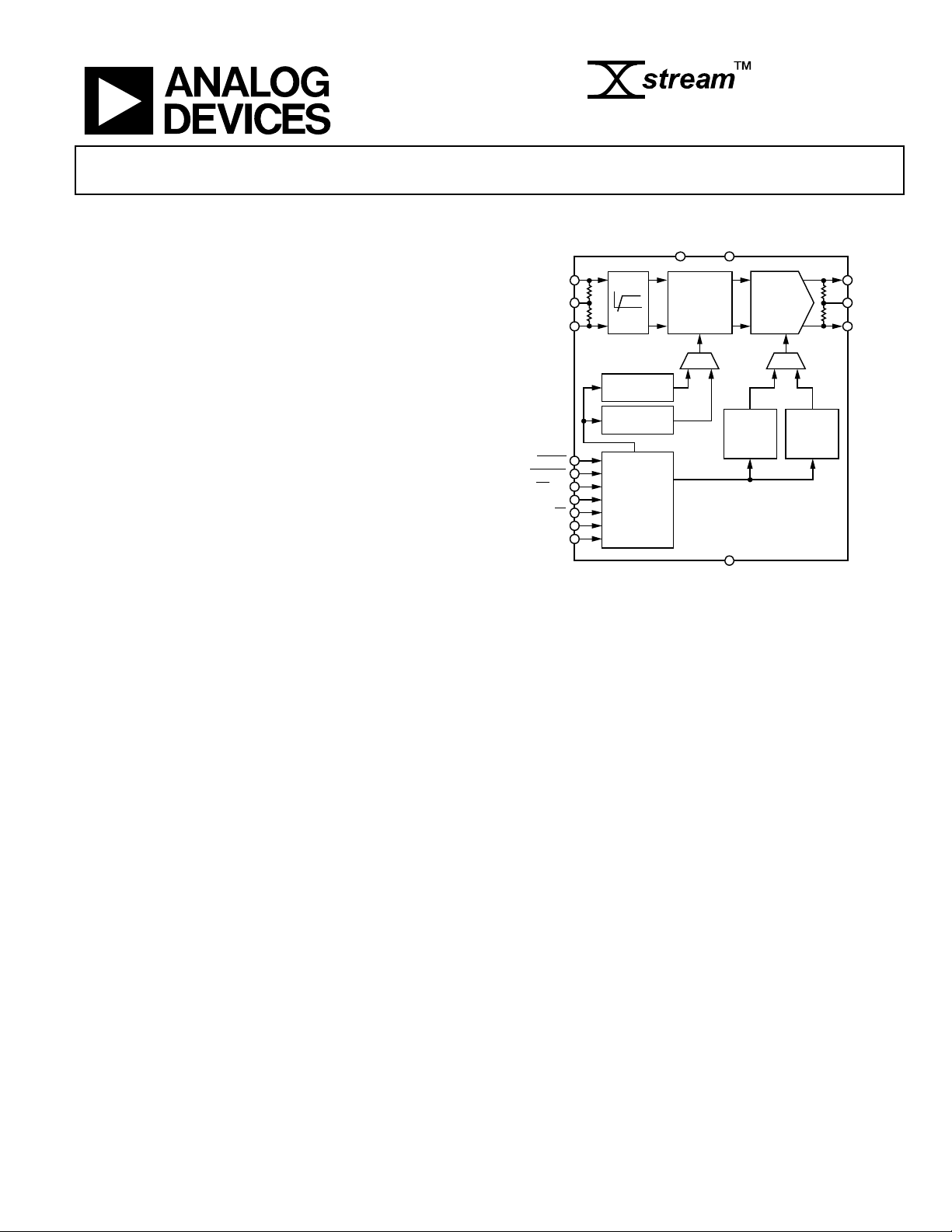
FUNCTIONAL BLOCK DIAGRAM
IP[15:0]
V
TTIE
V
TTIW
IN[15:0]
RESET
UPDATE
I2C/SPI
ADDR1/SDI
ADDR0/CS
SDA/SDO
SCL/SCK
,
DV
RX TX
EQ
CONNECTION
MAP 0
CONNECTION
MAP 1
SERIAL
INTERFACE
CONTROL
LOGIC
CC
16 × 16
SWITCH
MATRIX
Figure 1.
CC
V
EE
oint Switch
ADN4604
PRE-
EMPHASIS
OUTPUT
LEVEL
HOOKUP
TABLE
PER-PORT
SETTINGS
ADN4604
OUTPUT
LEVEL
OP[15:0]
V
TTON
V
TTOS
ON[15:0]
,
07934-001
APPLICATIONS
Fiber optic network switching
High speed serial backplane routing to OC-48 with FEC
XAUI: 10GBASE-KX4
Gigabit Ethernet over backplane: 1000BASE-KX
1×, 2×, and 4× Fibre Channel
InfiniBand®
Digital video (HDMI, DVI, DisplayPort, 3G-/HD-/SD-SDI)
Data storage networks
GENERAL DESCRIPTION
The ADN4604 is a 16 × 16 asynchronous, protocol agnostic,
digital crosspoint switch, with 16 differential PECL-/CMLcompatible inputs and 16 differential CML outputs.
The ADN4604 is optimized for nonreturn-to-zero (NRZ) signaling with data rates of up to 4.25 Gbps per port. Each port
offers a fixed level of input equalization and programmable
output swing and output preemphasis.
The ADN4604 nonblocking switch core implements a 16 × 16
crossbar and supports independent channel switching through
the serial control interface. The ADN4604 has low latency and
very low channel-to-channel skew.
2
An I
C® or SPI interface is used to control the device and provide access to advanced features, such as additional levels of
preemphasis and output disable.
The ADN4604 is packaged in a 100-lead TQFP package and
operates from −40°C to +85°C.
Rev. 0
Information furnished by Analog Devices is believed to be accurate and reliable. However, no
responsibility is assumed by Analog Devices for its use, nor for any infringements of patents or other
rights of third parties that may result from its use. Specifications subject to change without notice. No
license is granted by implication or otherwise under any patent or patent rights of Analog Devices.
Trademarks and registered trademarks are the property of their respective owners.
One Technology Way, P.O. Box 9106, Norwood, MA 02062-9106, U.S.A.
Tel: 781.329.4700 www.analog.com
Fax: 781.461.3113 ©2009 Analog Devices, Inc. All rights reserved.
Page 2

ADN4604
TABLE OF CONTENTS
Features .............................................................................................. 1
Applications ....................................................................................... 1
Functional Block Diagram .............................................................. 1
General Description ......................................................................... 1
Revision History ............................................................................... 2
Specifications ..................................................................................... 3
Electrical Specifications ............................................................... 3
I2C Timing Specifications ............................................................ 4
SPI Timing Specifications ........................................................... 5
Absolute Maximum Ratings ............................................................ 6
ESD Caution .................................................................................. 6
Pin Configuration and Function Descriptions ............................. 7
Typical Performance Characteristics ........................................... 10
Theory of Operation ...................................................................... 16
Introduction ................................................................................ 16
Receivers ...................................................................................... 16
Switch Core ................................................................................. 17
Transmitters ................................................................................ 19
Termination ................................................................................. 23
I2C Serial Control Interface ........................................................... 24
Reset ............................................................................................. 24
I2C Data Write ............................................................................. 24
I2C Data Read .............................................................................. 25
SPI Serial Control Interface .......................................................... 26
Register Map ................................................................................... 28
Applications Information .............................................................. 32
Supply Sequencing ..................................................................... 34
Power Dissipation....................................................................... 34
Output Compliance ................................................................... 34
Printed Circuit Board (PCB) Layout Guidelines ................... 36
Outline Dimensions ....................................................................... 38
Ordering Guide .......................................................................... 38
REVISION HISTORY
10/09—Revision 0: Initial Version
Rev. 0 | Page 2 of 40
Page 3

ADN4604
SPECIFICATIONS
ELECTRICAL SPECIFICATIONS
VCC = 3.3 V, V
input swing = 800 mV p-p, T
Table 1.
Parameter Conditions Min Typ Max Unit
DYNAMIC PERFORMANCE
Data Rate (DR) per Channel (NRZ) DC 4.25 Gbps
Deterministic Jitter Data rate = 4.25 Gbps, no channel 20 ps p-p
Random Jitter RMS, no channel 1 ps rms
Residual Deterministic Jitter with
Receive Equalization
Data rate = 4.25 Gbps, 40 in. FR4, EQ boost = 12 dB 70 ps p-p
Residual Deterministic Jitter with
Transmit Preemphasis
Data rate = 4.25 Gbps, 40 in. FR4, PE boost = 6 dB 35 ps p-p
Propagation Delay Input to output, EQ boost = 12 dB 800 ps
Channel-to-Channel Skew ±50 ps
Switching Time Update logic switching to 50% output data 100 ns
Output Rise/Fall Time 20% to 80% 75 ps
INPUT CHARACTERISTICS
Differential Input Voltage Swing V
Input Voltage Range Single-ended absolute voltage level, VL V
OUTPUT CHARACTERISTICS
Output Voltage Swing Differential, PE boost = 0 dB, default output level, at dc 600 800 900 mV p-p diff
Output Voltage Range Single-ended absolute voltage level, VL V
Per-Port Output Current PE boost = 0 dB, default output level 16 mA
PE boost = 6 dB, default output level 32 mA
TERMINATION CHARACTERISTICS
Resistance Single-ended, V
Temperature Coefficient 0.025 Ω/°C
POWER SUPPLY
Operating Range
VCC V
DVCC V
V
TTIE
V
TTON
Supply Current Outputs disabled
ICC 95 110 mA
I
DVCC
I
+ I
TTIE
Supply Current All outputs enabled, ac-coupled I/O, 400 mV I/O swings
ICC 342 370 mA
I
DVCC
I
+ I
TTIE
Supply Current All outputs enabled, ac-coupled I/O, 400 mV I/O swings
ICC 486 540 mA
I
DVCC
I
+ I
TTIE
= 3.3 V, V
TTIx
= 3.3 V, DVCC = 3.3 V, VEE = 0 V, RL = 50 Ω, data rate = 4.25 Gbps, ac-coupled inputs and outputs, differential
TTOx
= 27°C, unless otherwise noted.
A
Data rate = 4.25 Gbps, 20 in. FR4, EQ boost = 12 dB 27 ps p-p
Data rate = 4.25 Gbps, 30 in. FR4, EQ boost = 12 dB 43 ps p-p
Data rate = 4.25 Gbps, 20 in. FR4, PE boost = 4.2 dB 23 ps p-p
Data rate = 4.25 Gbps, 30 in. FR4, PE boost = 6 dB 25 ps p-p
1
= VCC − 0.6 V; VCC = V
ICM
Single-ended absolute voltage level, VH V
Single-ended absolute voltage level, VH V
= 2.2 V to 3.6 V, TA = T
V
TTO
= 0 V 2.7 3.3 3.6 V
EE
= 0 V 2.7 3.3 3.6 V
EE
, V
V
TTIW
, V
V
TTOS
= 0 V 1.3 3.3 VCC + 0.3 V
EE
= 0 V 2.22 3.3 VCC + 0.3 V
EE
= 2.7 V to 3.6 V, V
CC
MIN
MIN
to V
to T
, TA = T
MAX
MAX
MIN
= 2.2 V to 3.6 V,
TTI
;
to T
200 2000 mV p-p diff
MAX
+ 1.1 V
EE
+ 0.3 V
CC
– 1.3 V
CC
+ 0.2 V
CC
44 50 56 Ω
20 35 mA
+ I
+ I
TTIW
TTON
0 10 mA
TTOS
(800 mV p-p differential), PE boost = 0 dB,
20 35 mA
+ I
+ I
TTIW
TTON
256 280 mA
TTOS
50 Ω far-end terminations
(800 mV p-p differential), PE boost = 6 dB,
20 35 mA
+ I
+ I
TTIW
TTON
512 540 mA
TTOS
50 Ω far-end terminations
Rev. 0 | Page 3 of 40
Page 4
ADN4604
Parameter Conditions Min Typ Max Unit
THERMAL CHARACTERISTICS
Operating Temperature Range −40 +85 °C
θJA Still air; JEDEC 4-layer test board 24.9 °C/W
θJB Still air 11.6 °C/W
θJC At the exposed pad 0.95 °C/W
LOGIC CHARACTERISTICS
Input High Voltage Threshold (VIH) DVCC = 3.3 V 0.7 × VCC VCC V
Input Low Voltage Threshold (VIL) DVCC = 3.3 V VEE 0.3 × VCC V
Output High Voltage (VOH) 2 kΩ pull-up resistor to DVCC DVCC V
Output Low Voltage (VOL) IOL = 3 mA VEE 0.4 V
1
V
is the input common-mode voltage.
ICM
2
Minimum V
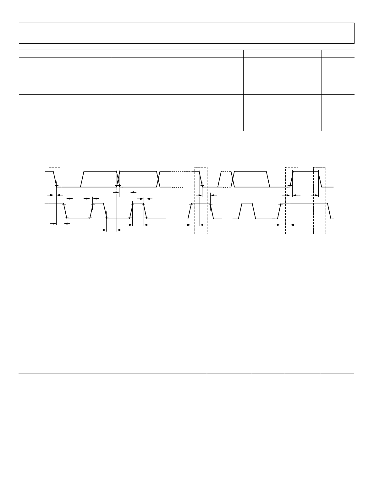
I2C TIMING SPECIFICATIONS
is only applicable for a limited range of output current settings. Refer to the Power Dissipation section.
TTO
SDA
t
SU:DAT
t
f
t
f
SCL
t
f
t
LOW
t
HD:STA
t
f
t
BUF
t
HD:STA
t
HD:DAT
t
HIGH
t
SU:STA
Figure 2. I
2
C Timing Diagram
t
SU:STO
SPSrS
07934-002
Table 2. I
2
C Timing Specifications
Parameter Symbol Min Max Unit
SCL Clock Frequency f
Hold Time for a Start Condition t
Setup Time for a Repeated Start Condition t
Low Period of the SCL Clock t
High Period of the SCL Clock t
Data Hold Time t
Data Setup Time t
Rise Time for Both SDA and SCL t
Fall Time for Both SDA and SCL t
Setup Time for Stop Condition t
Bus-Free Time Between a Stop Condition and a Start Condition t
0 400+ kHz
SCL
HD;STA
SU;STA
LOW
HIGH
HD;DAT
SU;DAT
r
f
SU;STO
BUF
0.6 μs
0.6 μs
1.3 μs
0.6 μs
0 μs
10 ns
1 300 ns
1 300 ns
0.6 μs
1 ns
Bus Idle Time After a Reset 10 ns
Reset Pulse Width 10 ns
Rev. 0 | Page 4 of 40
Page 5
ADN4604
SPI TIMING SPECIFICATIONS
CS
SCK
SDI
t
1
A7
t
2
t
3
A6 A5 A4 A3 A2 A1 A0 D7 D6 D5 D4 D3 D2 D1 D0
t
t
5
6
t
7
SDO
t
4
XXXXXXXXXXXXXXX X
t
8
07934-003
Figure 3. SPI Write Timing Diagram
t
9
CS
SCK
SDI
SDO
t
1
A7
X
t
2
t
3
A6 A5 A4 A3 A2 A1 A0 D7 D6 D5 D4 D3 D2 D1 D0
X X X X X X X D7D6D5D4D3D2D1 D0
t
t
5
6
t
4
t
7
t
8
07934-004
Figure 4. SPI Read Timing Diagram
Table 3. SPI Timing Specifications
Parameter Symbol Min Max Unit
SCK Clock Frequency f
CS to SCK Setup Time
0 10 MHz
SCK
10 ns
t
1
SCK High Pulse Width t2 40 ns
SCK Low Pulse Width t3 40 ns
Data Access Time After SCK Falling Edge t4 35 ns
Data Setup Time Prior to SCK Rising Edge t5 20 ns
Data Hold Time After SCK Rising Edge t6 10 ns
CS to SCK Hold Time
CS to SDO High Impedance
CS High Pulse Width
t
10
7
40
t
8
10
t
9
ns
ns
ns
Rev. 0 | Page 5 of 40
Page 6
ADN4604
ABSOLUTE MAXIMUM RATINGS
Table 4.
Parameter Rating
VCC to VEE 3.7 V
DVCC to VEE 3.7 V
V
, V
V
TTIE
TTIW
V
, V
TTON
V
TTOS
Internal Power Dissipation1 4.9 W
Differential Input Voltage 2.0 V
Logic Input Voltage VEE – 0.3 V < VIN < VCC + 0.6 V
Storage Temperature Range −65°C to +125°C
Lead Temperature Range 300°C
Junction Temperature 150°C
1
Internal power dissipation is for the device in free air.
T
= 27°C; θJA = 24.9°C/W in still air.
A
+ 0.6 V
CC
+ 0.6 V
CC
Stresses above those listed under Absolute Maximum Ratings
may cause permanent damage to the device. This is a stress
rating only; functional operation of the device at these or any
other conditions above those indicated in the operational
section of this specification is not implied. Exposure to absolute
maximum rating conditions for extended periods may affect
device reliability.
ESD CAUTION
Rev. 0 | Page 6 of 40
Page 7

ADN4604
PIN CONFIGURATION AND FUNCTION DESCRIPTIONS
RESET
IP0
IN0
V
IP1
IN1
V
TTIW
IP2
IN2
V
IP3
IN3
V
IP4
IN4
V
IP5
IN5
V
TTIW
IP6
IN6
V
IP7
IN7
UPDATE
CC
OP1599ON15
DV
98
100
1
PIN 1
2
3
4
CC
5
6
7
8
9
10
EE
11
12
13
CC
14
15
16
EE
17
18
19
20
21
22
CC
23
24
25
26
27
28
29
EE
V
OP0
ON0
I2C/SPI
TTON
EE
OP1496ON1497V
95
32
30
31
OP1
ON1
TTOS
V
CC
OP1290ON1291V
OP1393ON1394V
89
92
ADN4604
TOP VIEW
(Not to Scale)
36
33
34
35
37 38
CC
V
OP2
ON2
EE
V
OP3
ON3
CC
EE
OP1187ON1188V
86
40
41
39
CC
V
OP4
ON4
TTON
OP1084ON1085V
83
42
43
44
OP5
ON5
TTOS
V
EE
OP981ON982V
80
45
46
47
EE
V
OP6
ON6
SCL/SCK77OP878ON879V
76
75
74
73
72
71
70
69
68
67
66
65
64
63
62
61
60
59
58
57
56
55
54
53
52
51
48
49
50
OP7
ON7
ADDR1/SDI
NOTES
1. THE ADN4604 TQFP HAS AN EXPO SED PADDLE (EP AD) ON THE UNDERSIDE OF THE PACKAG E THAT AIDS
IN HEAT DISS IPATION. THE EPAD MUST BE E LECTRICALLY CONNECTED T O THE V
TO MEET THERMAL SPE CIFICATIONS.
2. SDA/SCL/ADDR1/0 FOR I
SCK/SDO/S DI/CS FOR S PI OPERATI ON.
2
C OPERATIO N.
SUPPLY PLANE
EE
Figure 5. Pin Configuration
SDA/SDO
IN15
IP15
V
CC
IN14
IP14
V
TTIE
IN13
IP13
V
EE
IN12
IP12
V
CC
IN11
IP11
V
EE
IN10
IP10
V
TTIE
IN9
IP9
V
CC
IN8
IP8
ADDR0/CS
07934-005
Rev. 0 | Page 7 of 40
Page 8
ADN4604
Table 5. Pin Function Descriptions
Pin No. Mnemonic Type Description
1
RESET
2 IP0 Input High Speed Input.
3 IN0 Input High Speed Input Complement.
Power Positive Supply.
4, 13, 22, 35, 41, 54, 63,
V
CC
72, 85, 91
5 IP1 Input High Speed Input.
6 IN1 Input High Speed Input Complement.
7, 19 V
Power
TTIW
8 IP2 Input High Speed Input.
9 IN2 Input High Speed Input Complement.
Power Negative Supply.
10, 16, 29, 38, 47, 60, 66,
V
EE
79, 88, 97, EPAD
11 IP3 Input High Speed Input.
12 IN3 Input High Speed Input Complement.
14 IP4 Input High Speed Input.
15 IN4 Input High Speed Input Complement.
17 IP5 Input High Speed Input.
18 IN5 Input High Speed Input Complement.
20 IP6 Input High Speed Input.
21 IN6 Input High Speed Input Complement.
23 IP7 Input High Speed Input.
24 IN7 Input High Speed Input Complement.
25
26
UPDATE
I2C
/SPI
27 OP0 Output High Speed Output.
28 ON0 Output High Speed Output Complement.
30 OP1 Output High Speed Output.
31 ON1 Output High Speed Output Complement.
32, 44 V
Power Output Termination Supply (South). These pins are normally tied to the V
TTOS
33 OP2 Output High Speed Output.
34 ON2 Output High Speed Output Complement.
36 OP3 Output High Speed Output.
37 ON3 Output High Speed Output Complement.
39 OP4 Output High Speed Output.
40 ON4 Output High Speed Output Complement.
42 OP5 Output High Speed Output.
43 ON5 Output High Speed Output Complement.
45 OP6 Output High Speed Output.
46 ON6 Output High Speed Output Complement.
48 OP7 Output High Speed Output.
49 ON7 Output High Speed Output Complement.
50 ADDR1/SDI Control I2C Slave Address Bit 1 (MSB) or SPI Data Input.
51
ADDR0/CS
52 IP8 Input High Speed Input.
53 IN8 Input High Speed Input Complement.
55 IP9 Input High Speed Input.
56 IN9 Input High Speed Input Complement.
Control
Control
Control I
Control I
Configuration Registers Reset, Active Low. This pin is normally pulled up
.
to DV
CC
Input Termination Supply (West). These pins are normally tied to the
V
pins.
TTIE
Second Rank Write Enable, Active Low. This pin is normally pulled up
to DV
.
CC
2
C/SPI Control Interface Selection, I2C Active Low.
2
C Slave Address Bit 0 (LSB) or SPI Chip Select (Active Low).
Rev. 0 | Page 8 of 40
TTON
pins.
Page 9

ADN4604
Pin No. Mnemonic Type Description
57, 69 V
58 IP10 Input High Speed Input.
59 IN10 Input High Speed Input Complement.
61 IP11 Input High Speed Input.
62 IN11 Input High Speed Input Complement.
64 IP12 Input High Speed Input.
65 IN12 Input High Speed Input Complement.
67 IP13 Input High Speed Input.
68 IN13 Input High Speed Input Complement.
70 IP14 Input High Speed Input.
71 IN14 Input High Speed Input Complement.
73 IP15 Input High Speed Input.
74 IN15 Input High Speed Input Complement.
75 SDA/SDO Control I2C Data or SPI Data Output.
76 SCL/SCK Control I2C Clock or SPI Clock.
77 OP8 Output High Speed Output.
78 ON8 Output High Speed Output Complement.
80 OP9 Output High Speed Output.
81 ON9 Output High Speed Output Complement.
82, 94 V
83 OP10 Output High Speed Output.
84 ON10 Output High Speed Output Complement.
86 OP11 Output High Speed Output.
87 ON11 Output High Speed Output Complement.
89 OP12 Output High Speed Output.
90 ON12 Output High Speed Output Complement.
92 OP13 Output High Speed Output.
93 ON13 Output High Speed Output Complement.
95 OP14 Output High Speed Output.
96 ON14 Output High Speed Output Complement.
98 OP15 Output High Speed Output.
99 ON15 Output High Speed Output Complement.
100 DVCC Power Digital Positive Supply.
Power Input Termination Supply (East). These pins are normally tied to the V
TTIE
Power
TTON
Output Termination Supply (North). These pins are normally tied to
TTOS
pins.
the V
TTIW
pins.
Rev. 0 | Page 9 of 40
Page 10
ADN4604
V
V
V
V
V
TYPICAL PERFORMANCE CHARACTERISTICS
VCC = 3.3 V, V
input swing = 800 mV p-p, T
= 3.3 V, V
TTIx
= 3.3 V, DVCC = 3.3 V, V
TTOx
= 27°C, unless otherwise noted.
A
= 0 V, RL = 50 Ω, data rate = 4.25 Gbps, ac-coupled inputs and outputs, differential
EE
200mV/DI
0.167IU/DIV
REFERENCE EYE DIAGRAM AT TP1
DATA OUT
PATTERN
GENERATOR
50Ω CABLES
2 2
INPUT
PIN
ADN4604
AC-COUPLED
EVALUATION
OUTPUT
BOARD
50Ω CABLES
2 2
PIN
50Ω
TP2TP1
OSCILLOSCOPE
HIGH SPEED
SAMPLING
07934-006
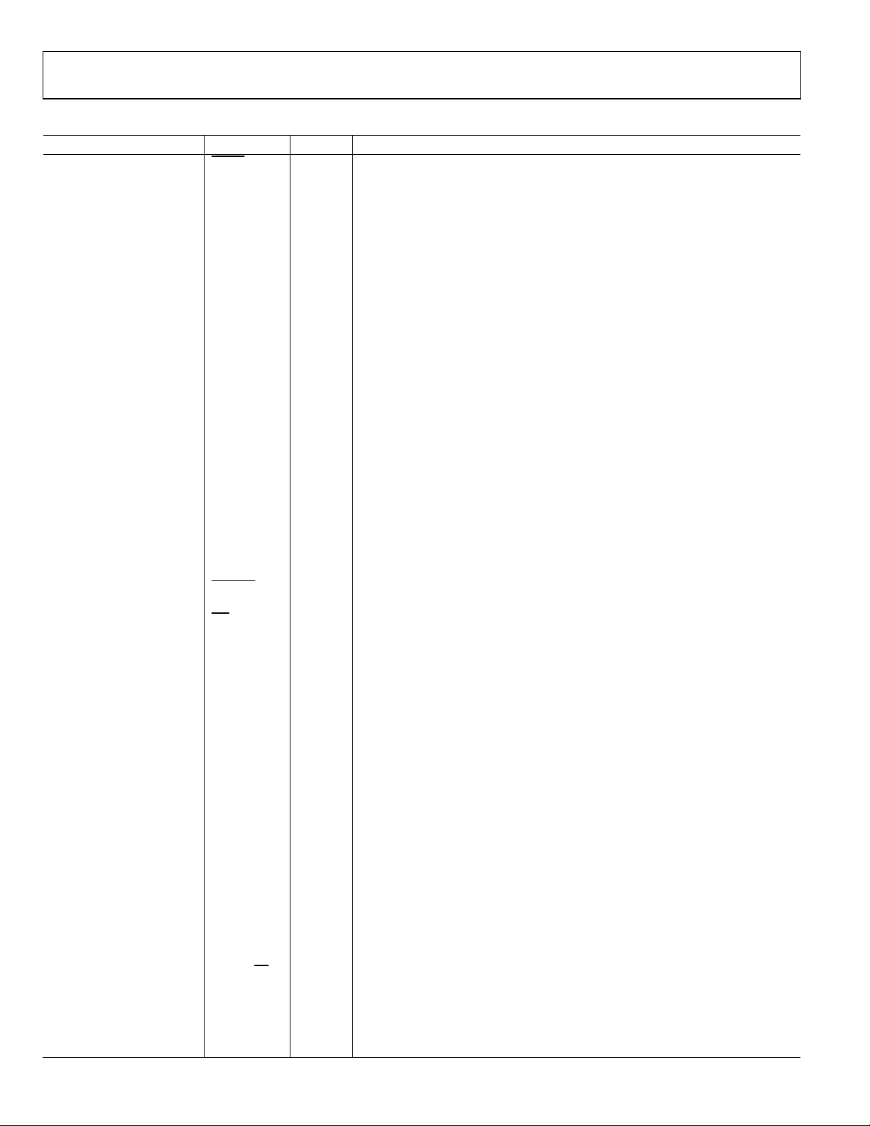
Figure 6. Standard Test Circuit
200mV/DI
0.167IU/DIV
Figure 7. 3.25 Gbps Input Eye (TP1 from Figure 6)
07934-007
200mV/DI
0.167IU/DIV
Figure 9. 3.25 Gbps Output Eye (TP2 from Figure 6)
07934-009
200mV/DI
0.167IU/DIV
Figure 8. 4.25 Gbps Input Eye (TP1 from Figure 6)
07934-008
200mV/DI
0.167IU/DIV
Figure 10. 4.25 Gbps Output Eye (TP2 from Figure 6)
4-010
0793
Rev. 0 | Page 10 of 40
Page 11
ADN4604
V
V
V
V
V
200mV/DI
RE
0.167IU/DIV
FERENCE EYE DIAGRAM AT TP1
DATA OUT
PATTERN
GENERATOR
50Ω CABLES
2 2
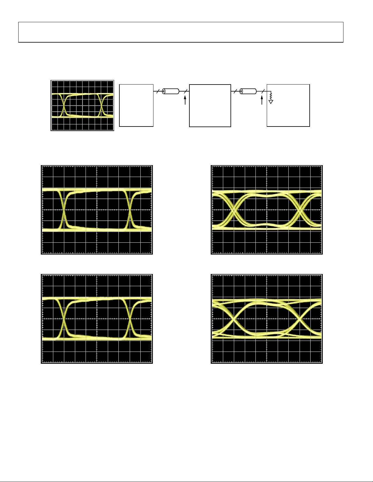
Figure 11. Equalization Test Circuit
FR4 TEST BACKP LANE
DIFFERENTIAL
STRIPLI NE TRACES
TP1
8mils WI DE, 8mils S P ACE ,
8mils DIEL ECTRIC HEI GHT
LENGTHS = 10 INCHES, 20 INCHES ,
30 INCHES, 40 I NCHES
50Ω CABLES
2 2
TP2
INPUT
OUTPUT
PIN
ADN4604
AC-COUPLED
EVALUATION
BOARD
2 2
PIN
50Ω CABLES
TP3
50Ω
HIGH
SPEED
SAMPLING
OSCILLOSCOPE
07934-011
200mV/DI
0.167IU/DIV
Figure 12. 4.25 Gbps Input Eye, 20 Inch FR4 Input Channel
(TP2 from Figure 11)
200mV/DI
0.167IU/DIV
Figu re 13. 4.25 Gb ps Input Eye, 40-Inch FR4 Input Channel
(TP2 from Figure 11)
200mV/DI
07934-012
0.167IU/DIV
07934-014
Figure 14. 4.25 Gbps Output Eye, 20-Inch FR4 Input Channel, EQ = 12 dB
(TP3 from Figure 11)
200mV/DI
07934-013
0.167IU/DIV
07934-015
Figure 15. 4.25 Gbps Output Eye, 40-Inch FR4 Input Channel, EQ = 12 dB
(TP3 from Figure 11)
Rev. 0 | Page 11 of 40
Page 12
ADN4604
V
V
V
V
V
200mV/DI
0.167IU/DIV
REFERENCE EYE DIAGRAM AT TP1
DATA OUT
PATTERN
GENERATOR
50Ω CABLES
2 2
Figure 16. Preemphasis Test Circuit
TP1
INPUT
OUTPUT
PIN
ADN4604
AC-COUPLED
EVALUATION
BOARD
50Ω CABLES
2 2
PIN
FR4 TEST BACKPLANE
DIFFERENTIAL
STRIPLI NE T RACES
TP2
8mils WI DE , 8mils SP ACE,
8mils DIEL ECTRIC HEI GHT
LENGTHS = 10 INCHES, 20 INCHES,
30 INCHES, 40 INCHE S
50Ω CABLES
2 2
TP3
50Ω
HIGH
SPEED
SAMPLING
OSCILLOSCOPE
07934-016
200mV/DI
0.167IU/DIV
07934-017
Figu re 17. 4.25 G bps Ou tput Eye, 20-Inch FR4 Out put Channel, PE = 0 dB
(TP3 from Figure 16)
200mV/DI
0.167IU/DIV
07934-018
Figure 18. 4.25 Gbps Output Eye, 40-Inch FR4 Input Channel, PE = 0 dB
(TP3 from Figure 16)
200mV/DI
0.167IU/DIV
07934-019
Figure 19. 4.25 Gbps Output Eye, 20-Inch FR4 Input Channel, PE = 4.2 dB
(TP3 from Figure 16)
200mV/DI
0.167IU/DIV
07934-020
Figure 20. 4.25 Gbps Output Eye, 40-Inch FR4 Input Channel, PE = 6 dB
(TP3 from Figure 16)
Rev. 0 | Page 12 of 40
Page 13

ADN4604
100
80
60
40
DETERMINISTIC JITTER (ps)
20
0
012345
DATA RATE (Gbps)
EQ = 0dB
EQ = 12dB
Figure 21. Deterministic Jitter vs. Data Rate
07934-036
1000
900
800
700
600
500
400
300
EYE HEIGHT (mV p-p DIFF)
200
100
0
012345
DATA RATE (Gbps)
Figure 24. Eye Height vs. Data Rate
07934-029
100
80
60
40
EQ = 0dB
DETERMINISTIC JITTER (ps)
20
0
2.52.62.72.82.93.03.13.23.33.4 3.63.5
EQ = 12dB
SUPPLY VOLTAGE (V)
Figure 22. Deterministic Jitter vs. Supply Voltage
100
80
60
40
DETERMINISTIC JITTER (ps)
20
0
–40 –20 0 20 40 60 80
EQ = 0dB
EQ = 12dB
TEMPERATURE (°C)
Figure 23. Deterministic Jitter vs. Temperature
1000
900
800
700
600
500
400
300
EYE HEIGHT (mV p-p DIFF)
200
100
407934-03
0
2.7 2.8 2.9 3.0 3.1 3.2 3.3 3.4 3.5 3.6
SUPPLY VOLTAGE (V)
07934-028
Figure 25. Eye Height vs. Supply Voltage
1000
900
800
700
600
500
400
300
EYE HEIGHT (mV p-p DIFF)
200
100
0
–40 –15 10 35 60 85
07934-035
TEMPERATURE (°C)
07934-037
Figure 26. Eye Height vs. Temperature
Rev. 0 | Page 13 of 40
Page 14

ADN4604
100
90
80
70
60
50
40
30
DETERMINISTIC JITTER (ps)
20
10
0
0 10203040
EQ = 0dB
EQ = 12dB
INPUT FR4 TRACE LENGTH (Inches)
Figure 27. Deterministic Jitter vs. Input FR4 Channel Length
100
80
60
100
90
80
70
60
50
40
30
DETERMINISTIC JITTER (ps)
20
10
0
0
934-031
07
10 20 30
0dB
4.2dB
2dB
OUTPUT FR4 TRACE LENGTH (Inches)
6dB
40 50 60 70
7.8dB
12dB
9.5dB
07934-030
Figure 30. Deterministic Jitter vs. Output FR4 Channel Length
100
80
60
40
EQ = 0dB
DETERMINISTIC JITTER (ps)
20
0
00.5
EQ = 12dB
1.0 1.5 2.0
DIFFERENTIAL INPUT SWING (V p-p)
Figure 28. Deterministic Jitter vs. Differential Input Swing
90
80
70
60
50
40
30
DETERMINISTIC JITTER (ps)
20
10
0
1.8 2.0 2.2 2.4 2.6 2.8 3.0 3.2 3.4 3.6
OUTPUT T E RM I NATION VOLTAGE V
OUTPUT LEVEL = 1200mV p-p DIF F
OUTPUT LEVEL = 800mV p-p DIFF
OUTPUT LEVEL = 200mV p-p DIFF
(V)
TTOx
Figure 29. Deterministic Jitter vs. Output Termination Voltage (V
TTO
40
EQ = 0dB
DETERMINI STIC JIT TER (ps)
20
0
0.9 1.2 1.5 1.8 2.1 2.4 2.7 3.0 3.3 3.6
07934-033
INPUT COMMON-MODE VOLTAGE (V)
EQ = 12dB
07934-032
Figure 31. Deterministic Jitter vs. Input Common-Mode Voltage
0
–2
–4
–6
–8
–10
LOSS (dB)
–12
–14
6"
–16
10"
20"
–18
30"
40"
–20
07934-025
)
FREQUENCY (Hz)
Figure 32. S21 Test Traces
1G100M10M1M100k
07934-038
Rev. 0 | Page 14 of 40
Page 15

ADN4604
A
A
100
90
80
70
FALL TIME
60
50
40
RISE/FALL TIME (ps)
30
20
10
0
–40 –20 0 20 40 60 80
RISE TIME
TEMPERATURE (°C)
Figure 33. Rise/Fall Time vs. Temperature
07934-026
500,000
450,000
400,000
350,000
300,000
250,000
SAMPLES
200,000
150,000
100,000
50,000
0
–7 –6 –5 –4 –2–3 –10123456
JITTER (ps)
Figure 36. Random Jitter Histogram
07934-024
1000
950
900
850
800
Y (ps)
750
700
DEL
650
600
550
500
2.7 2.8 2.9 3.0 3.1 3.2 3.3 3.4 3.5 3.6
EQ = 0
EQ = 12dB
SUPPLY VOLTAGE (V)
Figure 34. Propagation Delay vs. Supply Voltage
25
20
15
HITS
10
5
0
750 760 770 780 790 800 810 820 830 840
PROPAGATION DELAY (ps)
Figure 35. Propagation Delay Histogram
1000
950
900
850
800
Y (ps)
750
DEL
700
650
600
550
500
02307934-
–40 –30 –20 –10 0 10 20 30 40 50 60 70 80
EQ = 0dB
TEMPERATURE (°C)
EQ = 12dB
07934-022
Figure 37. Propagation Delay vs. Temperature
5
0
–5
–10
–15
–20
–25
–30
RETURN LOSS (d B)
–35
–40
–45
–50
10M 100M 1G 10G
07934-021
XAUI_SPEC
S22
S11
FREQUENCY ( Hz )
07934-027
Figure 38. Return Loss (S11, S22)
Rev. 0 | Page 15 of
40
Page 16

ADN4604
V
THEORY OF OPERATION
INTRODUCTION
The ADN4604 is a 16 × 16, buffered, asynchronous crosspoint
switch that provides input equalization, output preemphasis,
and output level programming capabilities. The receivers
integrate an equalizer that is optimized to compensate for
typical backplane losses. The switch supports multicast and
broadcast operation, allowing the ADN4604 to work in
redundancy and port-replication applications. The part offers
extensively programmable output levels and preemphasis
settings.
DV
IP[15:0]
V
TTIE
V
TTIW
IN[15:0]
RESET
UPDATE
I2C/SPI
ADDR1/SDI
ADDR0/CS
SDA/SDO
SCL/SCK
,
RX TX
EQ
CONNECTION
MAP 0
CONNECTION
MAP 1
SERIAL
INTERFACE
CONTROL
LOGIC
SWITCH
Figure 39. Block Diagram
The configuration of the crosspoint is controlled through
a serial interface. This interface supports both I
protocols, which can be selected using the
control pin. There are two I
2
described in . Tab le 6
Table 6. Serial Interface Control Modes
I2C
/SPI = 0
Pin
No.
Pin
Name
50 ADDR1
Pin
Functio n
2
C Address
I
MSB
51 ADDR0
2
C Address
I
LSB
75 SDA I2C Data SDO
76 SCL I2C Clock SCK SPI Clock
CC
16 × 16
MATRIX
CC
EMPHASIS
OUTPUT
LEVEL
HOOKUP
TABLE
PRE-
PER-PORT
OUTPUT
LEVEL
SETTINGS
ADN4604
V
EE
2
C and SPI
I2C
/SPI dedicated
C address pins available as
I2C
/SPI = 1
Pin
Name
SDI
Pin
Functio n
SPI Data
Input
CS SPI Chip
Select
SPI Data
Output
OP[15:0]
V
TTON
V
TTOS
ON[15:0]
RECEIVERS
Input Structure and Input Levels
The ADN4604 receiver inputs incorporate 50 termination
resistors, ESD protection, and a fixed equalizer that is optimized for
operation over long backplane traces. Each receive channel also
provides a positive/negative (P/N) inversion function, which allows
the user to swap the sign of the input signal path to eliminate the
need for board-level crossovers in the receiver channel.
V
CC
V
TTIx
,
IPx
INx
V
EE
Equalization
The ADN4604 receiver incorporates a continuous time equalizer
(EQ) that provides 12 dB of high frequency boost to compensate
up to 40 inches of FR4 at 4.25 Gbps. Each input has an equalizer
control bit. By default, the programmable boost is set to 12 dB.
The boost can be set to 0 dB by programming a Logic 0 to the
07934-039
respective register bit for the corresponding channel.
Table 7. Equalization Control Registers
EQ[15:0] Equalization Boost
0 0 dB
1 12 dB (default)
Lane Inversion
The receiver P/N inversion is a feature intended to allow the
user to implement the equivalent of a board-level crossover in
a much smaller area and without additional via impedance
discontinuities that degrade the high frequency integrity of the
signal path. The P/N inversion is available independently for
each of the 16 input channels and is controlled by writing to the
SIGN bit of the RX control registers (Addresses 0x12 and
Address 0x13). Note that using this feature to account for signal
inversions downstream of the receiver requires additional
attention when switching connectivity.
Table 8. Signal Path Polarity Control
SIGN[15:0] Signal Path Polarity
0 Noninverting (default)
1 Inverting
SIMPLIFIED RECEIVER INPUT CIRCUIT
52Ω
RP
RN
52Ω
R1
750Ω
R2
750Ω
R3
1kΩ
Figure 40. Simplified Input Circuit
RLN
Q1
Q2
RLP
RL
I1
07934-040
RL
Rev. 0 | Page 16 of 40
Page 17

ADN4604
SWITCH CORE
The ADN4604 switch core is a fully nonblocking 16 × 16 array
that allows multicast and broadcast configurations. The configuration of the switch core is programmed through the serial
control interface. The crosspoint configuration map controls
the connectivity of the switch core. The crosspoint configuration
map consists of a double-rank register architecture where each
rank consists of an 8-byte configuration map as shown in
Figure 41. The second rank registers contain the current state of
the crosspoint. The first rank registers contain the next state.
Each entry in the connection map stores four bits per output,
which indicates which of the 16 inputs are connected to a given
output. An entire connectivity matrix can be programmed at
once by passing data from the first rank registers into the
second rank registers.
The first rank registers are two separate volatile 8-byte memory
banks which store connection configurations for the crosspoint. Map 0 is the default map and is located at Address 0x90
to Address 0x97. By default, Map 0 contains a diagonal
connection configuration whereby Input 15 is connected to
Output 0, Input 14 to Output 1, Input 13 to Output 2, and so
on. Similarly, by default, Map 1 contains the opposite diagonal
connection configuration where Input 0 is connected to output
0, Input 1 to Output 1, and so on. Both maps are read/write
accessible registers. The active map is selected by writing to
the XPT table select register (Address 0x81).
FIRST RANK REG ISTERS
The crosspoint is configured by addressing the register
assigned to the desired output and writing the desired
connection data into the first rank of latches in either Map 0
or Map 1. The connection data is equivalent to the binary
coded value of the input number. This process is repeated until
each of the desired connections is programmed.
In situations where multiple outputs are to be programmed to
a single input, a broadcast command is available. A broadcast
command is issued by writing the binary value of the desired
input to the XPT broadcast register (Address 0x82). The broadcast is applied to the selected map as selected in the map table
select register (Address 0x81).
All output connections are updated simultaneously by passing
the data from the first rank of latches into the second rank by
writing 0x01 to the XPT update register (Address 0x80). This
is a write-only register. Alternatively, the
UPDATE
pin can be
strobed low. Otherwise, this pin should be left high.
The current state of the crosspoint connectivity is available
by reading the XPT status registers (Address 0xB0 to Address
0xB7). Register descriptions for the Map 0, Map 1 and XPT
status registers are provided in Tab l e 9. A complete register
map is provided in Table 18.
XPT MAP 0
015
0
INPUTS
15
REGIST E R 0x9 0 TO REGISTER 0x97
015
0
INPUTS
15
REGIST E R 0 x98 TO REGI S TER 0x9F
OUTPUTS
XPT MAP 1
OUTPUTS
SECOND RANK REGIST E RS
0
1
MAP TABLE
SELECT
REGISTER 0x81
UPDATE PIN
UPDATE
REGISTER 0x80
REGISTER 0xB0 TO REGISTER 0xB7
Figure 41. Crosspoint Connection Map Block Diagram
XPT STATUS READ
XPT CORE
015
0
INPUTS
15
OUTPUTS
07934-041
Rev. 0 | Page 17 of 40
Page 18

ADN4604
Table 9. XPT Control Registers
Register Name Address Bit Bit Name Description Default
Update 0x80 0 UPDATE Updates XPT switch core (active high, write only) N/A
Map Table Select 0x81 0 MAP TABLE SELECT 0: Map 0 is selected 0x00
1: Map 1 is selected
XPT Broadcast 0x82 3:0 BROADCAST[3:0] All outputs connection assignment, write only N/A
XPT Map 0 Control 0 0x90 7:4 OUT1[3:0] Output 1 connection assignment 0xEF
3:0 OUT0[3:0] Output 0 connection assignment
XPT Map 0 Control 1 0x91 7:4 OUT3[3:0] Output 3 connection assignment 0xCD
3:0 OUT2[3:0] Output 2 connection assignment
XPT Map 0 Control 2 0x92 7:4 OUT5[3:0] Output 5 connection assignment 0xAB
3:0 OUT4[3:0] Output 4 connection assignment
XPT Map 0 Control 3 0x93 7:4 OUT7[3:0] Output 7 connection assignment 0x89
3:0 OUT6[3:0] Output 6 connection assignment
XPT Map 0 Control 4 0x94 7:4 OUT9[3:0] Output 9 connection assignment 0x67
3:0 OUT8[3:0] Output 8 connection assignment
XPT Map 0 Control 5 0x95 7:4 OUT11[3:0] Output 11 connection assignment 0x45
3:0 OUT10[3:0] Output 10 connection assignment
XPT Map 0 Control 6 0x96 7:4 OUT13[3:0] Output 13 connection assignment 0x23
3:0 OUT12[3:0] Output 12 connection assignment
XPT Map 0 Control 7 0x97 7:4 OUT15[3:0] Output 15 connection assignment 0x01
3:0 OUT14[3:0] Output 14 connection assignment
XPT Map 1 Control 0 0x98 7:4 OUT1[3:0] Output 1 connection assignment 0x10
3:0 OUT0[3:0] Output 0 connection assignment
XPT Map 1 Control 1 0x99 7:4 OUT3[3:0] Output 3 connection assignment 0x32
3:0 OUT2[3:0] Output 2 connection assignment
XPT Map 1 Control 2 0x9A 7:4 OUT5[3:0] Output 5 connection assignment 0x54
3:0 OUT4[3:0] Output 4 connection assignment
XPT Map 1 Control 3 0x9B 7:4 OUT7[3:0] Output 7 connection assignment 0x76
3:0 OUT6[3:0] Output 6 connection assignment
XPT Map 1 Control 4 0x9C 7:4 OUT9[3:0] Output 9 connection assignment 0x98
3:0 OUT8[3:0] Output 8 connection assignment
XPT Map 1 Control 5 0x9D 7:4 OUT11[3:0] Output 11 connection assignment 0xBA
3:0 OUT10[3:0] Output 10 connection assignment
XPT Map 1 Control 6 0x9E 7:4 OUT13[3:0] Output 13 connection assignment 0xDC
3:0 OUT12[3:0] Output 12 connection assignment
XPT Map 1 Control 7 0x9F 7:4 OUT15[3:0] Output 15 connection assignment 0xFE
3:0 OUT14[3:0] Output 14 connection assignment
XPT Status 0 0xB0 7:4 OUT1[3:0] Output 1 connection status, read only 0xEF
3:0 OUT0[3:0] Output 0 connection status, read only
XPT Status 1 0xB1 7:4 OUT3[3:0] Output 3 connection status, read only 0xCD
3:0 OUT2[3:0] Output 2 connection status, read only
XPT Status 2 0xB2 7:4 OUT5[3:0] Output 5 connection status, read only 0xAB
3:0 OUT4[3:0] Output 4 connection status, read only
XPT Status 3 0xB3 7:4 OUT7[3:0] Output 7 connection status, read only 0x89
3:0 OUT6[3:0] Output 6 connection status, read only
XPT Status 4 0xB4 7:4 OUT9[3:0] Output 9 connection status, read only 0x67
3:0 OUT8[3:0] Output 8 connection status, read only
XPT Status 5 0xB5 7:4 OUT11[3:0] Output 11 connection status, read only 0x45
3:0 OUT10[3:0] Output 10 connection status, read only
XPT Status 6 0xB6 7:4 OUT13[3:0] Output 13 connection status, read only 0x23
3:0 OUT12[3:0] Output 12 connection status, read only
XPT Status 7 0xB7 7:4 OUT15[3:0] Output 15 connection status, read only 0x01
3:0 OUT14[3:0] Output 14 connection status, read only
Rev. 0 | Page 18 of 40
Page 19

ADN4604
TRANSMITTERS
Output Structure and Output Levels
The ADN4604 transmitter outputs incorporate 50 Ω termination resistors, ESD protection, and output current switches.
Each channel provides independent control of both the absolute
output level and the preemphasis output level. Note that the
choice of output level affects the output common-mode level.
V
ESD
RP
50Ω
Q1
Q2
IT
+ I
I
DC
PE
ON-CHIP TERM INATION
RN
50Ω
V3
VC
V2
VP
V1
VN
Figure 42. Simplified TX Output Circuit
Preemphasis
Transmission line attenuation can be equalized at the transmitter using preemphasis. The transmit equalizer setting can
be chosen by matching the channel loss to the amount of boost
provided by the preemphasis.
Basic Settings
In the basic mode of operation, predefined preemphasis settings
are available through a lookup table. Each table entry requires
two bytes of memory. The amount of preemphasis provided
is independent of the full-scale current output. Transmitter
preemphasis levels, as well as dc output levels, can be set
through the serial control interface. The output level and
amount of preemphasis can be independently programmed
through advanced registers. By default, however, the total
output amplitude and preemphasis setting space is reduced
to a single table of basic settings that provides eight levels of
output equalization to ease programming for typical FR4
channels.
Tabl e 10 summarizes the absolute output level, preemphasis
level, and high frequency boost for control setting. The full
resolution of eight settings is available through the serial
interface by writing to Bits[2:0] (the TX PE[2:0] bits) of the
Basic TX Control registers shown in Tabl e 11 . A single setting
is programmed to all outputs simultaneously by writing to the
0x18 broadcast address.
The TX has four possible output enable states (disabled,
standby, squelched, and enabled) controlled by the TX EN[1:0]
bits as shown in Ta ble 1 1. Disabled is the lowest power-down
state. When squelched, the output voltage at both P and N
outputs will be the common-mode voltage as defined by the
output current settings. In standby, the output level of both P
and N outputs will be pulled up to the termination supply
(V
TTON
or V
TTOS
).
CC
V
TTOx
OPx
ONx
V
EE
07934-042
The TX CTL SELECT bit (Bit 6) in the TX[15:0] basic control
register determines whether the preemphasis and output
current controls for the channel of interest are selected from
the predefined lookup table or directly from the TX[15:0]
Drive Control[1:0] registers (per channel). Figure 43 is an
illustration of the TX control circuit. Setting the TX CTL
SELECT bit low (default setting) selects preemphasis control
from the predefined, optimized lookup table (Address 0x60
to Address 0x6F).
LOOKUPTABLE
BASIC SETTINGS
TABLE
ENTRY 0
TABLE
ENTRY 1
TABLE
ENTRY 2
TABLE
ENTRY 3
TABLE
ENTRY 4
TABLE
ENTRY 5
TABLE
ENTRY 6
TABLE
ENTRY 7
PE[2:0]
PER PORT
OUTPUT LEVEL
ADVANCED SETTINGS
Figure 43. Transmitter Control Block Diagram
16
16
16
16
16
16
16
16
16
IPx
INx
16
3
SELECT
PER OUTPUT PORT
16
TX CTL
OPx
TX
ONx
2
TX EN[1:0]
In applications where the default preemphasis settings in the
lookup table are not sufficient, the lookup table entries can be
modified by programming the TX lookup table registers (0x60
to 0x6F) shown in Tabl e 12. In applications where the eight
table entries are insufficient, each output can be programmed
individually.
Table 10. Preemphasis Boost and Overshoot vs. Setting
PE
Setting
0 16 0 0.0 0 800
1 16 2 2.0 25 800
2 16 5 4.2 62.5 800
3 16 8 6.0 100 800
4 11 8 7.8 145 550
5 8 8 9.5 200 400
6 4 6 12.0 300 300
7 4 6 12.0 300 300
Main Tap
Current
(mA)
Delayed Tap
Current (mA)
Boost
(dB)
Overshoot
(%)
DC Swing
(mV p-p)
07934-043
Rev. 0 | Page 19 of 40
Page 20

ADN4604
Tabl e 11 displays the TX Basic Control register. The TX Basic Control register consists of one byte (8 bits) for each of the 16 output
channels. Each TX Basic Control register has the same functionality. The mapping of register address to output channel is shown in the
first column.
Table 11. TX Basic Control Register
Address: Channel Default Register Name Bit Bit Name Description
0x18: Broadcast,
0x20: Output 0,
0x21: Output 1,
0x22: Output 2,
0x23: Output 3,
0x24: Output 4,
0x25: Output 5,
0x26: Output 6,
0x27: Output 7,
0x28: Output 8,
0x29: Output 9,
0x2A: Output 10,
0x2B: Output 11,
0x2C: Output 12,
0x2D: Output 13,
0x2E: Output 14,
0x2F: Output 15
0x00 TX basic control 6 TX CTL SELECT
5:4 TX EN[1:0] 00: TX disabled, lowest power state
01: TX standby.
10: TX squelched.
11: TX enabled
3 Reserved Reserved. Set to 0.
2:0 PE[2:0]
Tabl e 12 displays the TX lookup table register. The TX lookup table register consists of two bytes (16 bits) for each of the eight possible
table entries selected by the PE[2:0] field in Tab le 1 1. The mapping of table entry to register address is shown in the first column. By
default, the TX Lookup Table register contains the preemphasis settings listed in Tabl e 10 , however, these values can be changed for a
flexible selection of output levels and preemphasis boosts. Table 1 3 lists a variety of possible output level and preemphasis boost settings
and the corresponding TX Drive 0 and TX Drive 1 codes.
0: PE and output level control is derived from
common lookup table
1: PE and output level control is derived from per port
drive control registers
If TX CTL SELECT = 0, see Table 10
000: Table Entry 0
001: Table Entry 1
010: Table Entry 2
011: Table Entry 3
100: Table Entry 4
101: Table Entry 5
110: Table Entry 6
111: Table Entry 7
If TX CTL SELECT = 1, PE[2:0] are ignored
Table 12. TX Lookup Table Registers
Address: Channel Default Register Name Bit Bit Name Description
0x60: Table Entry 0 0xFF
0x62: Table Entry 1 0xFF
0x64: Table Entry 2 0xFF 6:4 DRV LV1[2:0] Driver 1 current = decimal(DRV LV1[2:0]) + 1
0x66: Table Entry 3 0xFF
0x68: Table Entry 4 0xDC 3 DRV EN0
0x6A: Table Entry 5 0xBB
0x6C: Table Entry 6 0x99 2:0 DRV LV0[2:0] Driver 0 current = decimal(DRV LV0[2:0]) + 1
0x6E: Table Entry 7 0x99
0x61: Table Entry 0 0x00
0x63: Table Entry 1 0x99
0x65: Table Entry 2 0xCC 6:4 DRV LVD[2:0] Driver D Current = decimal(DRV LVD[2:0]) + 1
0x67: Table Entry 3 0xFF
0x69: Table Entry 4 0xFF 3 DRV EN2
0x6B: Table Entry 5 0xFF
0x6D: Table Entry 6 0xDD 2:0 DRV LV2[2:0] Driver 2 current = decimal(DRV LV2[2:0]) + 1
0x6F: Table Entry 7 0xDD
TX Lookup
Table Drive 0
TX Lookup
Table Drive 1
7 DRV EN1
7 DRV END
0: Driver 1 disabled
1: Driver 1 enabled
0: Driver 0 disabled
1: Driver 0 enabled
0: Driver D disabled
1: Driver D enabled
0: Driver 2 disabled
1: Driver 2 enabled
Rev. 0 | Page 20 of 40
Page 21

ADN4604
V
Advanced Settings
In addition to the basic settings provided in the TX basic
control registers, advanced settings are available in TX Drive 0
Control and TX Drive 1 Control registers (Address 0x30 to
Address 0x4F). The advanced settings are useful in applications
where each output requires an individually programmed
preemphasis or output level setting beyond what is available
in the lookup table in basic mode. To enable these advanced
settings, set the TX CTL SELECT bit in the TX basic control
register to a logic high. Next, program the TX Drive 0 control
and Drive 1 control registers (Address 0x30 to Address 0x4F) to
the desired output level and boost values. A subset of possible
settings is provided in Table 13. An expanded list of available
settings is shown in Tabl e 19 in the Applications Information
section. These advanced settings can also be used to modify the
TX lookup table settings (Address 0x60 to Address 0x6F). The
advanced settings register map is shown in Tabl e 15 .
The preemphasis boost equation follows.
−
VV
(1)
DCSWPESW
−−
Gain
TTO
V
OCM
+×=
10
T
PE
V
)1(log20]dB[
DCSW
−
V
H-PE
V
H-DC
V
L-DC
SW-PE
V
L-PE
07934-044
V
SW-DC
V
Figure 44. Signal Level Definitions
Table 14. Symbol Definitions
Symbol Formula Definition
IDC Programmable Output current that sets output level
IPE Programmable Output current for PE delayed tap
I
I
TTO
+ IPE Total transmitter output current
DC
TPE Preemphasis pulse width
V
25 Ω × I
DPP-DC
V
25 Ω × I
DPP-PE
V
V
SW-DC
V
V
SW-PE
∆V
OCM_DC-COUPLED
∆V
OCM_AC-COUPLED
V
V
OCM
V
V
H-DC
V
V
L-DC
V
V
H-PE
V
V
L-PE
V
Output termination voltage
TTO
25 Ω × I
50 Ω × I
DPP-DC
DPP-PE
TTO
TTO
TTO
TTO
TTO
× 2
DC
× 2
TTO
/2 = V
/2 = V
− ∆V
− ∆V
− ∆V
− ∆V
− ∆V
– V
H-DC
H-PE
/2 Output common-mode shift, dc-coupled outputs
TTO
/2 Output common-mode shift, ac-coupled outputs
TTO
= ( V
OCM
+ V
OCM
− V
OCM
+ V
OCM
− V
OCM
DC single-ended voltage swing
L-DC
– V
Preemphasized single-ended voltage swing
L-PE
+ V
H-DC
DPP-DC
DPP-DC
DPP-PE
DPP-PE
)/2 Output common-mode voltage
L-DC
/2 DC single-ended output high voltage
/2 DC single-ended output low voltage
/2 Maximum single-ended output voltage
/2 Minimum single-ended output voltage
Table 13. TX Preemphasis and Output Swing Advanced
Settings
Single-Ended Output Levels and
PE Boost
V
SW-DC1
(mV)
V
SW-PE
(mV)
1
PE Boost % PE
(dB)
200 200 0.00 0.00 0xBB 0x00 8
200 300 50.00 3.52 0xBB 0x99 12
200 350 75.00 4.86 0xBB 0xAA 14
200 400 100.00 6.02 0xBB 0xBB 16
200 450 125.00 7.04 0xBB 0xCC 18
200 500 150.00 7.96 0xBB 0xDD 20
200 600 200.00 9.54 0xBB 0xFF 24
300 300 0.00 0.00 0xDD 0x00 12
300 400 33.33 2.50 0xDD 0x99 16
300 450 50.00 3.52 0xDD 0xAA 18
300 500 66.67 4.44 0xDD 0xBB 20
300 550 83.33 5.26 0xDD 0xCC 22
300 600 100.00 6.02 0xDD 0xDD 24
300 700 133.33 7.36 0xDD 0xFF 28
400 400 0.00 0.00 0xFF 0x00 16
400 500 25.00 1.94 0xFF 0x99 20
400 550 37.50 2.77 0xFF 0xAA 22
400 600 50.00 3.52 0xFF 0xBB 24
400 650 62.50 4.22 0xFF 0xCC 26
400 700 75.00 4.86 0xFF 0xDD 28
400 800 100.00 6.02 0xFF 0xFF 32
500 500 0.00 0.00 0xFF 0x0B 20
600 600 0.00 0.00 0xFF 0x0F 24
1
Symbol definitions are shown in Table 14.
TX
Drive 0
Register
Settings
TX
Drive 1 I
Output
Current
1
(mA)
TTO
Peak-to-peak differential voltage swing of nonpreemphasized waveform
Peak-to-peak differential voltage swing of preemphasized
waveform
Rev. 0 | Page 21 of 40
Page 22

ADN4604
Tabl e 15 displays the TX advanced control registers. The TX advanced control registers consist of two bytes (16 bits) for each of the 16
output channels. The mapping of register address to output channel is shown in the first column. The TX advanced control registers
provides ultimate flexibility of per port output level and preemphasis boost. Tab l e 1 3 lists a variety of possible output levels and
preemphasis boost settings and the corresponding TX Drive 0 and TX Drive 1 codes.
Table 15. TX Advanced Control Registers
Address: Channel Default Register Name Bit Bit Name Description
0x30: Output 0,
0x32: Output 1,
0x34: Output 2,
0x36: Output 3,
0x38: Output 4,
0x3A: Output 5,
0x3C: Output 6,
0x3E: Output 7,
0x40: Output 8,
0x42: Output 9,
0x44: Output 10,
0x46: Output 11,
0x48: Output 12,
0x4A: Output 13,
0x4C: Output 14,
0x4E: Output 15
0x31: Output 0,
0x33: Output 1,
0x35: Output 2,
0x37: Output 3,
0x39: Output 4,
0x3B: Output 5,
0x3D: Output 6,
0x3F: Output 7,
0x41: Output 8,
0x43: Output 9,
0x45: Output 10,
0x47: Output 11,
0x49: Output 12,
0x4B: Output 13,
0x4D: Output 14,
0x4F: Output 15
0xFF
0x00
TX Drive 0
control
TX Drive 1
control
7 DRV EN1 0: Driver 1 disabled
1: Driver 1 enabled
6:4 DRV LV1[2:0] Driver 1 current = decimal(DRV LV1[2:0]) + 1
3 DRV EN0 0: Driver 0 disabled
1: Driver 0 enabled
2:0 DRV LV0[2:0] Driver 0 current = decimal(DRV LV0[2:0]) + 1
7 DRV END 0: Driver D disabled
1: Driver D enabled
6:4 DRV LVD[2:0] Driver D current = decimal(DRV LVD[2:0]) + 1
3 DRV EN2 0: Driver 2 disabled
1: Driver 2 enabled
2:0 DRV LV2[2:0] Driver 2 current = decimal(DRV LV2[2:0]) + 1
Rev. 0 | Page 22 of 40
Page 23

ADN4604
V
VVV
TERMINATION
The inputs and outputs include integrated 50 termination
resistors. For applications that require external termination
resistors, the internal resistors can be disabled. For example,
disabling the integrated 50 termination resistors allows
alternative termination values such as 75 as shown in
Figure 45.
Note that the integrated 50 termination resistors are optimal
for high data rate digital signaling. Disabling the terminations
can reduce the overall performance.
TTIx TTIx CC TTOx
50Ω50Ω75Ω75Ω
The termination control is separated by quadrants (North =
Outputs[15:8], South = Outputs[7:0], East = Inputs[15:8], and
West = Inputs[7:0]).
Tabl e 16 shows the termination control register. A Logic 0
enables the terminations for the respective quadrant. A Logic 1
disables the terminations for the respective quadrant. The
terminations are enabled by default.
V
50Ω50Ω
TTOx
75Ω
75Ω
CML
ADN4604
V
EE
Figure 45. 75 Ω to 50 Ω Impedance Translator.
50Ω
50Ω
Table 16. Termination Control Register
Address Default Register Name Bit Bit Name Description
0xF0 0x00 Termination control 3 TXN_TERM
Output[15:8] (North) termination control
0: Terminations enabled
1: Terminations disabled
2 TXS_TERM Output[7:0] (South) termination control
0: Terminations enabled
1: Terminations disabled
1 RXE_TERM Input[15:8] (East) termination control
0: Terminations enabled
1: Terminations disabled
0 RXW_TERM Input[7:0] (West) termination control
0: Terminations enabled
1: Terminations disabled
50Ω
Rx
07934-045
Rev. 0 | Page 23 of 40
Page 24
ADN4604
I2C SERIAL CONTROL INTERFACE
The ADN4604 register set is controlled through a 2-wire I2C
interface. The ADN4604 acts only as an I
2
the I
C bus in the system needs to include an I2C master to
configure the ADN4604 and other I
the bus.
The ADN4604 I
2
C interface can be run in the standard
(100 kHz) and fast (400 kHz) modes. The SDA line only
changes value when the SCL pin is low with two exceptions. To
indicate the beginning or continuation of a transfer, the SDA
pin is driven low while the SCL pin is high; to indicate the end
of a transfer, the SDA line is driven high while the SCL line is
high. Therefore, it is important to control the SCL clock to
toggle only when the SDA line is stable unless indicating a start,
repeated start, or stop condition.
Table 17. I
2
C Device Address Assignment
ADDR1 Pin ADDR0 Pin I2C Device Address
0 0 0x90
0 1 0x92
1 0 0x94
1 1 0x96
RESET
On initial power-up, or at any point in operation, the ADN4604
register set can be restored to the default values by pulling the
RESET
pin to low according to the specification in
During normal operation, however, the
pulled up to DV
. A software reset is available by writing the
CC
value 0x01 to the Reset register at Address 0x00. This register is
write only.
I2C DATA WRITE
To write data to the ADN4604 register set, a microcontroller,
or any other I
signals to the ADN4604 slave device. The steps to be followed
are listed below; the signals are controlled by the I
unless otherwise specified. A diagram of the procedure is
shown in Figure 46.
2
C master, must send the appropriate control
2
C slave device. Therefore,
2
C devices that may be on
Tabl e 2.
RESET
pin must be
2
C master,
1. Send a start condition (while holding the SCL line high,
pull the SDA line low).
2. Send the ADN4604 part address (seven bits) whose upper
four bits are the static value b10010 and whose lower three
bits are controlled by the input pins I2C_A[1:0]. This
transfer should be MSB first.
3. Send the write indicator bit (0).
4. Wait for the ADN4604 to acknowledge the request.
5. Send the register address (eight bits) to which data is to be
written. This transfer should be MSB first.
6. Wait for the ADN4604 to acknowledge the request.
7. Send the data (eight bits) to be written to the register
whose address was set in Step 5. This transfer should be
MSB first.
8. Wait for the ADN4604 to acknowledge the request.
9. Do one or more of the following:
a. Send a stop condition (while holding the SCL line high,
pull the SDA line high) and release control of the bus.
b. Send a repeated start condition (while holding the
SCL line high, pull the SDA line low) and continue
with Step 2 of the write procedure to perform a write.
c. Send a repeated start condition (while holding the
SCL line high, pull the SDA line low) and continue
with Step 2 of this procedure to perform a read from
another address.
d. Send a repeated start condition (while holding the
SCL line high, pull the SDA line low) and continue
with Step 8 of the read procedure (in the I2C Data
Read section) to perform a read from the same
address set in Step 5.
The ADN4604 write process is shown in Figure 46. The SCL
signal is shown along with a general write operation and a
specific example. In the example, data 0x92 is written to
Address 0x6D of an ADN4604 part with a part address of 0x4B.
It is important to note that the SDA line only changes when the
SCL line is low, except for the case of sending a start, stop, or
repeated start condition, Step 1 and Step 9 in this case.
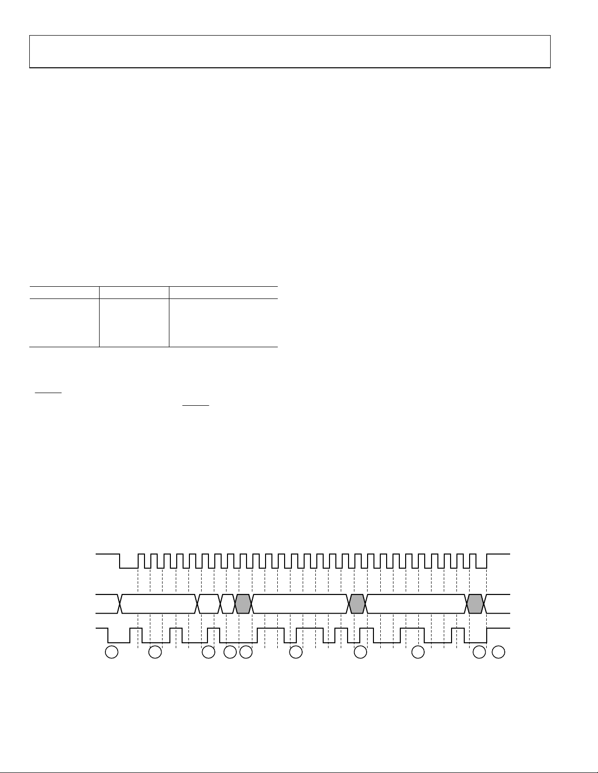
SCL
SDA
SDA
EXAMPLE
START R/W ACK AC K ACK STOPDATA
1 2 2 3 4 5 6 7 8 9a
b10010 REGISTER ADDR
ADDR
[1:0]
Figure 46. I
2
C Write Diagram
Rev. 0 | Page 24 of 40
07934-046
Page 25

ADN4604
I2C DATA READ
To read data from the ADN4604 register set, a microcontroller,
or any other I
signals to the ADN4604 slave device. The steps are listed below;
the signals are controlled by the I
specified. A diagram of the procedure is shown in Figure 47.
1. Send a start condition (while holding the SCL line high,
pull the SDA line low).
2. Send the ADN4604 part address (seven bits) whose upper
five bits are the static value b10010 and whose lower two
bits are controlled by the input pins ADDR1 and ADDR0.
This transfer should be MSB first.
3. Send the write indicator bit (0).
4. Wait for the ADN4604 to acknowledge the request.
5. Send the register address (eight bits) from which data is to
be read. This transfer should be MSB first. The register
address is kept in memory in the ADN4604 until the part
is reset or the register address is written over with the same
procedure (Step 1 to Step 6).
6. Wait for the ADN4604 to acknowledge the request.
7. Send a repeated start condition (while holding the SCL line
high, pull the SDA line low).
8. Send the ADN4604 part address (seven bits) whose upper
five bits are the static value b10010 and whose lower two
bits are controlled by the input pins ADDR1 and ADDR0.
This transfer should be MSB first.
9. Send the read indicator bit (1).
10. Wait for the ADN4604 to acknowledge the request.
11. The ADN4604 then serially transfers the data (eight bits)
held in the register indicated by the address set in Step 5.
12. Acknowledge the data.
2
C master must send the appropriate control
2
C master, unless otherwise
13. Do one or more of the following:
a. Send a stop condition (while holding the SCL line high
pull the SDA line high) and release control of the bus.
b. Send a repeated start condition (while holding the
SCL line high, pull the SDA line low) and continue
with Step 2 of the write procedure (see the I
2
C Data
Wr it e section) to perform a write.
c. Send a repeated start condition (while holding the
SCL line high, pull the SDA line low) and continue
with Step 2 of this procedure to perform a read from
another address.
d. Send a repeated start condition (while holding the
SCL line high, pull the SDA line low) and continue
with Step 8 of this procedure to perform a read from
the same address.
The ADN4604 read process is shown in Figure 47. The SCL
signal is shown along with a general read operation and a
specific example. In the example, Data 0x49 is read from
Address 0x6D of an ADN4604 part with a part address of 0x4B.
The part address is seven bits wide and is composed of the
ADN4604 static upper five bits (b10010) and the pin programmable lower two bits (ADDR1 and ADDR0). In this example,
the ADDR1 and ADDR0 bits are set to b01. In Figure 47, the
corresponding step number is visible in the circle under the
waveform. The SCL line is driven by the I
2
C master and never
by the ADN4604 slave. As for the SDA line, the data in the
shaded polygons is driven by the ADN4604, whereas the data in
the nonshaded polygons is driven by the I
2
C master. The end
phase case shown is that of 13a.
Note that the SDA line only changes when the SCL line is low,
except for the case of sending a start, stop, or repeated start
condition, as in Step 1, Step 7, and Step 13. In Figure 47, A is
the same as ACK in Figure 46. Equally, Sr represents a repeated
start where the SDA line is brought high before SCL is raised.
SDA is then dropped while SCL is still high.
SCL
SDA
SDA
EXAMPLE
ADDR
b10010 A A Sr DATA A STOPREGISTE R ADDRSTART
1 2 2 3 4 5 6 7 8 8 9 10 11 12 13a
[1:0]
R/
W
Figure 47. I
2
C Read Diagram
b10010
ADDR
[1:0]
R/
A
W
7934-047
Rev. 0 | Page 25 of 40
Page 26

ADN4604
O
O
SPI SERIAL CONTROL INTERFACE
The SPI serial interface of the ADN4604 consists of four wires:
CS
, SCK, SDI, and SDO. CS is used to select the device when
more than one device is connected to the serial clock and data
CS
lines.
commands (see ). SCK is used to clock data in and out
of the part. Data can either contain eight bits of register address
or data.
The SDI line is used to write to the registers, and the SDO line
is used to read data back from the registers. Data on SDI is
clocked on the rising edge of SCK. Data on SDO changes on the
falling edge of SCK. The recommended pull-up resistor value is
between 500 Ω and 1 kΩ. Strong pull-ups are needed when
serial clock speeds that are close to the maximum limit are used
or when the SPI interface lines are experiencing large capacitive
loading. Larger resistor values can be used for pull-up resistors
when the serial clock speed is reduced.
The part operates in slave mode and requires an externally
applied serial clock to the SCLK input. The serial interface is
designed to allow the part to be interfaced to systems that
provide a serial clock that is synchronized to the serial data.
Write Operation
Figure 48 shows the diagram for a write operation to the
ADN4604. Data is clocked into the registers on the rising edge
of SCK. When the
is also used to distinguish between read and write
Figure 48
CS
line is high, the SDI and SDO lines are in
CS
three-state mode. Only when the
goes from high to low does
the part accept any data on the SDI line. To allow continuous
writes, the address pointer register auto-increments by one
without having to load the address pointer register each time.
Subsequent data bytes are written into sequential registers. Note
that not all registers in the 256-byte address space exist and not
all registers are writable. Zeroes should be entered for
nonexisting address fields when implementing a continuous
write operation. Address 0xD0 to Address 0xEF are reserved
and should not be overwritten. A continuous write sequence is
shown in . Figure 49
Read Operation
Figure 48 shows the diagram for a write operation to the
ADN4604. To read back from a register, first write to the
address pointer register with the desired starting address. A
read command is distinguished from a write command by the
occurrence of
Subsequent clock cycles with
CS
going high after the address pointer is written.
CS
asserted low stream data
starting from the desired register address onto SDO, MSB first.
SDO changes on the falling edge of SCK.
Multiple data reads are possible in SPI interface mode as the
address pointer register is auto-incremented. A continuous read
sequence is shown in Figure 50.
CS
SDI
SD
CS
SDI
SD
ADDRESS DATA
HI-Z
WRITE OPERATION
ADDRESS XXXXXXXX
HI-Z
READ OPERAT I ON
Figure 48. SPI—Correct Use of
CS
During SPI Communications
DATA
07934-048
Rev. 0 | Page 26 of 40
Page 27

ADN4604
CS
SCK
SDI
SDO
ADDRESS DATA BYTE 0 DATA BYTE 1 DATA BYT E N
HI-Z
07934-049
Figure 49. SPI Continuous Write Sequence
CS
SCK
SDI
SDO
ADDRESS XXXXXXXX XXXXXXXX XXXXXXXX
HI-Z
DATA BY TE 0 DATA BY TE 1 DATA BYTE N
07934-050
Figure 50. SPI Continuous Read Sequence
Rev. 0 | Page 27 of 40
Page 28

ADN4604
REGISTER MAP
Registers repeated per port or per table entry are grouped together. Register address mapping is shown in the first column.
Table 18. Register Map
Address: Channel Default Register Name Bit Bit Name Description
0x00 N/A RESET 0 Reset Software reset. Write only.
0x10 0xFF RX EQ Control 0 7 EQ[7] Equalizer boost control for input 7
0: 0 dB
1: 12 dB
6 EQ[6] Equalizer boost control for Input 6
5 EQ[5] Equalizer boost control for Input 5
4 EQ[4] Equalizer boost control for Input 4
3 EQ[3] Equalizer boost control for Input 3
2 EQ[2] Equalizer boost control for Input 2
1 EQ[1] Equalizer boost control for Input 1
0 EQ[0] Equalizer boost control for Input 0
0x11 0xFF RX EQ Control 1 15 EQ[15] Equalizer boost control for Input 15
0: 0 dB
1: 12 dB
14 EQ[14] Equalizer boost control for Input 14
13 EQ[13] Equalizer boost control for Input 13
12 EQ[12] Equalizer boost control for Input 12
11 EQ[11] Equalizer boost control for Input 11
10 EQ[10] Equalizer boost control for Input 10
9 EQ[9] Equalizer boost control for Input 9
8 EQ[8] Equalizer boost control for Input 8
0x12 0x00 RX Control 0 7 SIGN[7] Signal path polarity inversion for Input 7
0: Noninverting
1: Inverting
6 SIGN[6] Signal path polarity inversion for Input 6
5 SIGN[5] Signal path polarity inversion for Input 5
4 SIGN[4] Signal path polarity inversion for Input 4
3 SIGN[3] Signal path polarity inversion for Input 3
2 SIGN[2] Signal path polarity inversion for Input 2
1 SIGN[1] Signal path polarity inversion for Input 1
0 SIGN[0] Signal path polarity inversion for Input 0
0x13 0x00 RX Control 1 15 SIGN[15] Signal path polarity inversion for Input 15
0: Noninverting
1: Inverting
14 SIGN[14] Signal path polarity inversion for Input 14
13 SIGN[13] Signal path polarity inversion for Input 13
12 SIGN[12] Signal path polarity inversion for Input 12
11 SIGN[11] Signal path polarity inversion for Input 11
10 SIGN[10] Signal path polarity inversion for Input 10
9 SIGN[9] Signal path polarity inversion for Input 9
8 SIGN[8] Signal path polarity inversion for Input 8
Rev. 0 | Page 28 of 40
Page 29

ADN4604
Address: Channel Default Register Name Bit Bit Name Description
0x18: Broadcast,
0x20: Output 0,
0x21: Output 1,
0x22: Output 2,
0x23: Output 3,
0x24: Output 4,
0x25: Output 5,
0x26: Output 6,
0x27: Output 7,
0x28: Output 8,
0x29: Output 9,
0x2A: Output 10,
0x2B: Output 11,
0x2C: Output 12,
0x2D: Output 13,
0x2E: Output 14,
0x2F: Output 15
0x30: Output 0,
0x32: Output 1,
0x34: Output 2,
0x36: Output 3,
0x38: Output 4,
0x3A: Output 5,
0x3C: Output 6,
0x3E: Output 7,
0x40: Output 8,
0x42: Output 9,
0x44: Output 10,
0x46: Output 11,
0x48: Output 12,
0x4A: Output 13,
0x4C: Output 14,
0x4E: Output 15
0x31: Output 0,
0x33: Output 1,
0x35: Output 2,
0x37: Output 3,
0x39: Output 4,
0x3B: Output 5,
0x3D: Output 6,
0x3F: Output 7,
0x41: Output 8,
0x43: Output 9,
0x45: Output 10,
0x47: Output 11,
0x49: Output 12,
0x4B: Output 13,
0x4D: Output 14,
0x4F: Output 15
0x60: Table Entry 0 0xFF
0x62: Table Entry 1 0xFF
0x64: Table Entry 2 0xFF 6:4 DRV LV1[2:0] Driver 1 current = decimal(DRV LV1[2:0]) + 1
0x66: Table Entry 3 0xFF
0x68: Table Entry 4 0xDC 3 DRV EN0
0x6A: Table Entry 5 0xBB
0x6C: Table Entry 6 0x99 2:0 DRV LV0[2:0] Driver 0 current = decimal(DRV LV0[2:0]) + 1
0x6E: Table Entry 7 0x99
0x00 TX basic control 6 TX CTL SELECT
5:4 TX EN[1:0] 00: TX disabled, lowest power state
01: TX standby
10: TX squelched
11: TX enabled
3 Reserved Reserved. Set to 0.
2:0 PE[2:0]
0xFF
0x00
TX Drive 0
control
TX Drive 1
control
TX Lookup
Table 0
7 DRV EN1 0: Driver 1 disabled
1: Driver 1 enabled
6:4 DRV LV1[2:0] Driver 1 current = decimal(DRV LV1[2:0]) + 1
3 DRV EN0 0: Driver 0 disabled
1: Driver 0 enabled
2:0 DRV LV0[2:0] Driver 0 current = decimal(DRV LV0[2:0]) + 1
7 DRV END 0: Driver D disabled
1: Driver D enabled
6:4 DRV LVD[2:0] Driver D current = decimal(DRV LVD[2:0]) + 1
3 DRV EN2 0: Driver 2 disabled
2:0 DRV LV2[2:0] Driver 2 current = decimal(DRV LV2[2:0]) + 1
7 DRV EN1
0: PE and output level control is derived from common
lookup table
1: PE and output level control is derived from per port
drive control registers
If TX CTL SELECT = 0, see Table 10
Selected table entry = decimal(PE[2:0])
If TX CTL SELECT = 1, PE[2:0] are ignored
1: Driver 2 enabled
0: Driver 1 disabled
1: Driver 1 enabled
0: Driver 0 disabled
1: Driver 0 enabled
Rev. 0 | Page 29 of 40
Page 30

ADN4604
Address: Channel Default Register Name Bit Bit Name Description
0x61: Table Entry 0 0x00
0x63: Table Entry 1 0x99
0x65: Table Entry 2 0xCC 6:4 DRV LVD[2:0] Driver D current = decimal(DRV LVD[2:0]) + 1
0x67: Table Entry 3 0xFF
0x69: Table Entry 4 0xFF 3 DRV EN2
0x6B: Table Entry 5 0xFF
0x6D: Table Entry 6 0xDD 2:0 DRV LV2[2:0] Driver 2 current = decimal(DRV LV2[2:0]) + 1
0x6F: Table Entry 7 0xDD
0x80 Write only Update 0 UPDATE Updates XPT switch core (active high, write only)
0x81 0x00 Map table select 0
0x82 Write only XPT broadcast 3:0 BROADCAST[3:0] All outputs connection assignment
0x90 0xEF
0x91 0xCD
0x92 0xAB
0x93 0x89
0x94 0x67
0x95 0x45
0x96 0x23
0x97 0x01
0x98 0x10
0x99 0x32
0x9A 0x54
0x9B 0x76
0x9C 0x98
0x9D 0xBA
0x9E 0xDC
0x9F 0xFE
TX Lookup
Table 1
XPT Map 0
Control 0
XPT Map 0
Control 1
XPT Map 0
Control 2
XPT Map 0
Control 3
XPT Map 0
Control 4
XPT Map 0
Control 5
XPT Map 0
Control 6
XPT Map 0
Control 7
XPT Map 1
Control 0
XPT Map 1
Control 1
XPT Map 1
Control 2
XPT Map 1
Control 3
XPT Map 1
Control 4
XPT Map 1
Control 5
XPT Map 1
Control 6
XPT Map 1
Control 7
7 DRV END
MAP TABLE
SELECT
7:4 OUT1[3:0] Output 1 connection assignment
3:0 OUT0[3:0] Output 0 connection assignment
7:4 OUT3[3:0] Output 3 connection assignment
3:0 OUT2[3:0] Output 2 connection assignment
7:4 OUT5[3:0] Output 5 connection assignment
3:0 OUT4[3:0] Output 4 connection assignment
7:4 OUT7[3:0] Output 7 connection assignment
3:0 OUT6[3:0] Output 6 connection assignment
7:4 OUT9[3:0] Output 9 connection assignment
3:0 OUT8[3:0] Output 8 connection assignment
7:4 OUT11[3:0] Output 11 connection assignment
3:0 OUT10[3:0] Output 10 connection assignment
7:4 OUT13[3:0] Output 13 connection assignment
3:0 OUT12[3:0] Output 12 connection assignment
7:4 OUT15[3:0] Output 15 connection assignment
3:0 OUT14[3:0] Output 14 connection assignment
0: Driver D disabled
1: Driver D enabled
0: Driver 2 disabled
1: Driver 2 enabled
0: Map 0 is selected
1: Map 1 is selected
Rev. 0 | Page 30 of 40
Page 31

ADN4604
Address: Channel Default Register Name Bit Bit Name Description
0xB0 0xEF XPT Status 0 7:4 OUT1[3:0] Output 1 connection status
3:0 OUT0[3:0] Output 0 connection status
0xB1 0xCD XPT Status 1 7:4 OUT3[3:0] Output 3 connection status
3:0 OUT2[3:0] Output 2 connection status
0xB2 0xAB XPT Status 2 7:4 OUT5[3:0] Output 5 connection status
3:0 OUT4[3:0] Output 4 connection status
0xB3 0x89 XPT Status 3 7:4 OUT7[3:0] Output 7 connection status
3:0 OUT6[3:0] Output 6 connection status
0xB4 0x67 XPT Status 4 7:4 OUT9[3:0] Output 9 connection status
3:0 OUT8[3:0] Output 8 connection status
0xB5 0x45 XPT Status 5 7:4 OUT11[3:0] Output 11 connection status
3:0 OUT10[3:0] Output 10 connection status
0xB6 0x23 XPT Status 6 7:4 OUT13[3:0] Output 13 connection status
3:0 OUT12[3:0] Output 12 connection status
0xB7 0x01 XPT Status 7 7:4 OUT15[3:0] Output 15 connection status
3:0 OUT14[3:0] Output 14 connection status
0xF0 0x00
0xFE Revision 7:0 REV[7:0] Read-only
0xFF 0x04 Device ID 7:0 ID[7:0] Read-only
Termination
control
3 TXN_TERM
2 TXS_TERM Output[7:0] (South) termination control
1 RXE_TERM Input[15:8] (East) termination control
0 RXW_TERM Input[7:0] (West) termination control
Output[15:8] (North) termination control
0: Terminations enabled
1: Terminations disabled
Rev. 0 | Page 31 of 40
Page 32

ADN4604
APPLICATIONS INFORMATION
The ADN4604 is an asynchronous and protocol agnostic digital
switch and, therefore, is applicable to a wide range of applications including network routing and digital video switching.
The ADN4604 supports the data rates and signaling levels of
HDMI®, DVI®, DisplayPort and SD-, HD-, and 3G-SDI digital
video. The ADN4604 can be used to create matrix switches. An
example block diagram of a 16 × 16 matrix switch is shown in
Figure 51. Since HDMI, DVI, and DisplayPort are quad lane
protocols, four ADN4604s are used to create a full 16 × 16
matrix switch. Smaller arrays, such as 4 × 4 and 8 × 8, require
one and two ADN4604 devices, respectively. Proper high speed
PCB design techniques should be used to maintain the signal
integrity of the high data rate signals. It is important to minimize
the lane-to-lane skew and crosstalk in these applications.
SOURCE 1
SOURCE 2
SOURCE 3
SOURCE 4
SOURCE 5
SOURCE 6
SOURCE 7
SOURCE 8
SOURCE 9
SOURCE 10
SOURCE 11
SOURCE 12
SOURCE 13
SOURCE 14
SOURCE 15
IN 0
IN 1
IN 15
IN 0
IN 1
IN 15
IN 0
IN 1
IN 15
IN 0
IN 1
ADN4604
ADN4604
ADN4604
ADN4604
OUT 0
OUT 1
OUT 15
OUT 0
OUT 1
OUT 15
OUT 0
OUT 1
OUT 15
OUT 0
OUT 1
DISPLAY 1
DISPLAY 2
DISPLAY 3
DISPLAY 4
DISPLAY 5
DISPLAY 6
DISPLAY 7
DISPLAY 8
DISPLAY 9
DISPLAY 10
DISPLAY11
DISPLAY 12
DISPLAY 13
DISPLAY 14
DISPLAY 15
SOURCE 16
IN 15
OUT 15
DISPLAY 16
07934-051
Figure 51. ADN4604 Digital Video (DVI, HDMI, DisplayPort) Matrix Switch Block Diagram
Rev. 0 | Page 32 of 40
Page 33

ADN4604
A
O/E CDR E/O
O/E CDR E/O
O/E CDR E/O
IN 1
IN 2
ADN4604
CROSSPOINT
SWITCH
IN 15
16 × 16
OUT 1
OUT 2
OUT 15
4-0520793
Figure 52. ADN4604 Networking Switch Application Block Diagram
TH
Z
0
Z
0
Z
0
Z
0
LOSSY CHANNE L
ASIC 2
07934-053
ASIC 1
8 LANE UPLINK P
Z
0
EQ PE
Z
0
8 LANE DOWNL INK PATH
Z
0
PE EQ
Z
0
LOSSY CHANNEL
Figure 53. Multi-Lane Signal Conditioning Application Diagram
Rev. 0 | Page 33 of 40
Page 34

ADN4604
V
SUPPLY SEQUENCING
Ideally, all power supplies should be brought up to the appropriate levels simultaneously (power supply requirements are set by
the supply limits in Ta b le 1 and the absolute maximum ratings
listed in Table 4 ). If the power supplies to the ADN4604 are
brought up separately, the supply power-up sequence is as follows:
DV
powered first, followed by VCC, and, last the termination
CC
supplies (V
sequence is reversed with termination supplies being powered
off first. The termination supplies contain ESD protection
diodes to the V
current condition in these devices (I
V
and V
TTI
should be powered off before V
If the system power supplies have a high impedance in the
powered off state, then supply sequencing is not required
provided the following limits are observed:
• Peak current from V
• Sustained current from V
POWER DISSIPATION
The power dissipation of the ADN4604 depends on the supply
voltages, I/O coupling type, and device configuration. The
input termination resistors dissipate power depending on the
differential input swing and common-mode voltage. When accoupled, the common-mode voltage is equal to the termination
supply voltage (V
the input termination supply is effectively zero, there is still
power and heat dissipated in the termination resistors as a result
of the differential signal swing. The core supply current and
output termination current are strongly dependent on device
configuration, such as the number of channels enabled, output
level setting, and output preemphasis setting.
In high ambient temperature operating conditions, it is important to avoid exceeding the maximum junction temperature of
the device. Limiting the total power dissipation can be achieved
by the following:
• Reducing the output swing
, V
, V
or V
, and V
TTON
or V
TTIx
TTIx
). While the current drawn from
TTIW
TTIE
TTIW
power domain. To avoid a sustained high
CC
supplies should be powered on after VCC and
TTO
TTIE
). The power-down
TTOS
SUSTAINED
.
CC
to VCC < 200 mA
TTOx
or V
TTOx
< 100 mA), the
to VCC < 100 mA
3.3
V
V
TTIx
CC
• Reducing the preemphasis level
• Decreasing the supply voltages within the allowable ranges
defined in Ta b le 1
• Disabling unused channels
Alternatively, the thermal resistance can be reduced by
• Adding an external heat-sink
• Increasing the airflow
Refer to the Printed Circuit Board (PCB) Layout Guidelines
section for recommendations for proper thermal stencil layout
and fabrication.
OUTPUT COMPLIANCE
In low voltage applications, users must pay careful attention
to both the differential and common-mode signal level. The
choice of output voltage swing, preemphasis setting, supply
voltages (V
peak and settled single-ended voltage swings and the commonmode shift measured across the output termination resistors.
These choices also affect output current and, consequently,
power consumption. Tab l e 1 9 shows the change in output
common mode (V
preemphasis setting. Single-ended output levels are calculated
for V
challenges of reducing the supply voltage. The minimum V
V
) cannot be below the absolute minimum level specified in
L
Tabl e 1. The combinations of output level, preemphasis, supply
voltage, and output coupling for which the minimum V
specification is violated are listed as N/A in Ta ble 1 .
Since the absolute minimum output voltage specified in Ta b le 1
is relative to V
output levels within the specified limits when lower output
termination voltages are required. V
are allowable for output swings less than or equal to 400 mV
(single-ended). Figure 54 illustrates an application where the
ADN4604 is used as a dc-coupled level translator to interface a
3.3 V CML driver to an ASIC with 1.8 V I/Os. The diode in
series with V
compliance.
1.8V3.3V
V
TTOx
and V
CC
supplies of 3.3 V and 2.5 V to illustrate practical
TTO
CC
reduces the voltage at VCC for improved output
CC
), and output coupling (ac or dc) affect
TTO
= VCC − V
OCM
) with output level and
OCM
, decreasing VCC is required to maintain the
voltages as low as 1.8 V
TTO
L
L
(min
1.8V
ASIC
3.3V
Z
0
CML
Z
0
Figure 54. DC-Coupled Level Translator Application Circuit
CML
ADN4604
V
EE
Rev. 0 | Page 34 of 40
Z
0
Rx
Z
0
07934-054
Page 35

ADN4604
Table 19. Output Voltage Range and Output Common-Mode Shift vs. Output Level and PE Setting
AC-Coupled Outputs DC-Coupled Outputs
Single-Ended Output Levels and
PE Boost
V
SW-DC1
(mV)
V
SW-PE
(mV)
1
PE Boost % PE
(dB)
100 100 0.00 0.00 0x99 0x00 4 100 3.25 3.15 2.45 2.35 50 3.3 3.2 2.5 2.4
100 150 50.00 3.52 0x99 0x88 6 150 3.225 3.075 2.425 2.275 75 3.3 3.15 2.5 2.35
100 200 100.00 6.02 0x99 0x99 8 200 3.2 3 2.4 2.2 100 3.3 3.1 2.5 2.3
100 250 150.00 7.96 0x99 0xAA 10 250 3.175 2.925 2.375 2.125 125 3.3 3.05 2.5 2.25
100 300 200.00 9.54 0x99 0xBB 12 300 3.15 2.85 2.35 2.05 150 3.3 3 2.5 2.2
100 350 250.00 10.88 0x99 0xCC 14 350 3.125 2.775 2.325 1.975 175 3.3 2.95 2.5 2.15
100 400 300.00 12.04 0x99 0xDD 16 400 3.1 2.7 2.3 1.9 200 3.3 2.9 2.5 2.1
100 450 350.00 13.06 0x99 0xEE 18 450 3.075 2.625 2.275 1.825 225 3.3 2.85 2.5 2.05
100 500 400.00 13.98 0x99 0xFF 20 500 3.05 2.55 2.25 1.75 250 3.3 2.8 2.5 2
200 200 0.00 0.00 0xBB 0x00 8 200 3.2 3 2.4 2.2 100 3.3 3.1 2.5 2.3
200 250 25.00 1.94 0xBB 0x88 10 250 3.175 2.925 2.375 2.125 125 3.3 3.05 2.5 2.25
200 300 50.00 3.52 0xBB 0x99 12 300 3.15 2.85 2.35 2.05 150 3.3 3 2.5 2.2
200 350 75.00 4.86 0xBB 0xAA 14 350 3.125 2.775 2.325 1.975 175 3.3 2.95 2.5 2.15
200 400 100.00 6.02 0xBB 0xBB 16 400 3.1 2.7 2.3 1.9 200 3.3 2.9 2.5 2.1
200 450 125.00 7.04 0xBB 0xCC 18 450 3.075 2.625 2.275 1.825 225 3.3 2.85 2.5 2.05
200 500 150.00 7.96 0xBB 0xDD 20 500 3.05 2.55 2.25 1.75 250 3.3 2.8 2.5 2
200 550 175.00 8.79 0xBB 0xEE 22 550 3.025 2.475 2.225 1.675 275 3.3 2.75 2.5 1.95
200 600 200.00 9.54 0xBB 0xFF 24 600 3 2.4 2.2 1.6 300 3.3 2.7 2.5 1.9
300 300 0.00 0.00 0xDD 0x00 12 300 3.15 2.85 2.35 2.05 150 3.3 3 2.5 2.2
300 350 16.67 1.34 0xDD 0x88 14 350 3.125 2.775 2.325 1.975 175 3.3 2.95 2.5 2.15
300 400 33.33 2.50 0xDD 0x99 16 400 3.1 2.7 2.3 1.9 200 3.3 2.9 2.5 2.1
300 450 50.00 3.52 0xDD 0xAA 18 450 3.075 2.625 2.275 1.825 225 3.3 2.85 2.5 2.05
300 500 66.67 4.44 0xDD 0xBB 20 500 3.05 2.55 2.25 1.75 250 3.3 2.8 2.5 2
300 550 83.33 5.26 0xDD 0xCC 22 550 3.025 2.475 2.225 1.675 275 3.3 2.75 2.5 1.95
300 600 100.00 6.02 0xDD 0xDD 24 600 3 2.4 2.2 1.6 300 3.3 2.7 2.5 1.9
300 650 116.67 6.72 0xDD 0xEE 26 650 2.975 2.325 2.175 1.525 325 3.3 2.65 2.5 1.85
300 700 133.33 7.36 0xDD 0xFF 28 700 2.95 2.25 2.15 1.45 350 3.3 2.6 2.5 1.8
400 400 0.00 0.00 0xFF 0x00 16 400 3.1 2.7 2.3 1.9 200 3.3 2.9 2.5 2.1
400 450 12.50 1.02 0xFF 0x88 18 450 3.075 2.625 2.275 1.825 225 3.3 2.85 2.5 2.05
400 500 25.00 1.94 0xFF 0x99 20 500 3.05 2.55 2.25 1.75 250 3.3 2.8 2.5 2
400 550 37.50 2.77 0xFF 0xAA 22 550 3.025 2.475 2.225 1.675 275 3.3 2.75 2.5 1.95
400 600 50.00 3.52 0xFF 0xBB 24 600 3 2.4 2.2 1.6 300 3.3 2.7 2.5 1.9
400 650 62.50 4.22 0xFF 0xCC 26 650 2.975 2.325 2.175 1.525 325 3.3 2.65 2.5 1.85
400 700 75.00 4.86 0xFF 0xDD 28 700 2.95 2.25 2.15 1.45 350 3.3 2.6 2.5 1.8
400 750 87.50 5.46 0xFF 0xEE 30 750 2.925 2.175 N/A2 N/A2 375 3.3 2.55 2.5 1.75
400 800 100.00 6.02 0xFF 0xFF 32 800 2.9 2.1 N/A2 N/A2 400 3.3 2.5 2.5 1.7
450 450 0.00 0.00 0xFF 0x09 18 450 3.075 2.625 2.275 1.825 225 3.3 2.85 2.5 2.05
450 650 44.44 3.19 0xFF 0xBD 26 650 2.975 2.325 2.175 1.525 325 3.3 2.65 2.5 1.85
500 500 0.00 0.00 0xFF 0x0B 20 500 3.05 2.55 N/A2 N/A2 250 3.3 2.8 2.5 2
500 700 40.00 2.92 0xFF 0xBF 28 700 2.95 2.25 2.15 1.45 350 3.3 2.6 2.5 1.8
550 550 0.00 0.00 0xFF 0x0D 22 550 3.025 2.475 2.225 1.675 275 3.3 2.75 2.5 1.95
550 650 18.18 1.45 0xFF 0x9F 26 650 2.975 2.325 2.175 1.525 325 3.3 2.65 2.5 1.85
600 600 0.00 0.00 0xFF 0x0F 24 600 3 2.4 N/A2 N/A2 300 3.3 2.7 2.5 1.9
1
Symbol definitions are shown in Table 14.
2
This setting is not allowed when ac-coupled with VCC = 2.7 V and V
TX
Drive 0
Register
Settings
TX
Drive 1
Output
Current
1
I
TTO
(mA)
TTON
V
1
∆V
V
OCM
(mV)
= 2.5 V or V
(V)
TTOS
= V
CC
TTO
1
H-PE
= 2.5 V.
= 3.3 V
V
1
L-PE
(V)
VCC = 2.7 V
V
= 2.5 V VCC = V
TTO
1
V
(V)
H-PE
1
V
L-PE
(V)
1
∆V
OCM
(mV)
= 3.3 V
TTO
1
V
V
H-DC
(V)
(V)
L-DC
V
= 2.5 V
TTO
1
V
(V)
H-PE
1
1
V
L-PE
(V)
VCC = 2.7 V
Rev. 0 | Page 35 of 40
Page 36

ADN4604
PRINTED CIRCUIT BOARD (PCB) LAYOUT GUIDELINES
The high speed differential inputs and outputs should be routed
with 100 controlled impedance differential transmission
lines. The transmission lines, either microstrip or stripline,
should be referenced to a solid low impedance reference plane.
An example of a PCB cross-section is shown in Figure 55. The
trace width (W), differential spacing (S), height above reference
plane (H), and dielectric constant of the PCB material determine
the characteristic impedance. Adjacent channels should be kept
apart by a distance greater than 3 W to minimize crosstalk.
WSW
SOLDERMASK
SIGNAL (M ICROSTRIP)
PCB DIELECTRI C
REFERENCE PLANE
PCB DIELECTRI C
SIGNAL (STRIPLINE)
PCB DIELECTRI C
REFERENCE PLANE
PCB DIELECTRI C
WSW
Figure 55. Example of a PCB Cross-Section
Thermal Paddle Design
The TQFP is designed with an exposed thermal paddle to
conduct heat away from the package and into the PCB. By
incorporating thermal vias into the PCB thermal paddle,
heat is dissipated more effectively into the inner metal layers
of the PCB. To ensure device performance at elevated
temperatures, it is important to have a sufficient number of
thermal vias incorporated into the design. An insufficient
number of thermal vias results in a θ
value larger than
JA
specified in Tabl e 1.
It is recommended that a via array of 4 × 4 or 5 × 5 with a
diameter of 0.3 mm to 0.33 mm be used to set a pitch between
1.0 mm and 1.2 mm. A representative of these arrays is shown in
Figure 56.
H
7934-055
Stencil Design for the Thermal Paddle
To effectively remove heat from the package and to enhance
electrical performance, the thermal paddle must be soldered
(bonded) to the PCB thermal paddle, preferably with minimum
voids. However, eliminating voids may not be possible because
of the presence of thermal vias and the large size of the thermal
paddle for larger size packages. Also, outgassing during the
reflow process may cause defects (splatter, solder balling) if the
solder paste coverage is too big.
It is recommended that smaller multiple openings in the stencil
be used instead of one big opening for printing solder paste on
the thermal paddle region. This typically results in 50% to 80%
solder paste coverage. Figure 57 shows how to achieve these
levels of coverage.
Voids within solder joints under the exposed paddle can have
an adverse affect on high speed and RF applications, as well as
on thermal performance. Because the package incorporates a
large center paddle, controlling solder voiding within this
region can be difficult. Voids within this ground plane can
increase the current path of the circuit. The maximum size for
a void should be less than via pitch within the plane. This
assures that any one via is not rendered ineffectual when any
void increases the current path beyond the distance to the next
available via.
1.35mm × 1.35mm SQUARES
AT 1.65mm PITCH
COVERAGE: 68%
07934-057
Figure 57. Typical Thermal Paddle Stencil Design
THERMAL
VIA
THERMAL
PADDLE
Figure 56. PCB Thermal Paddle and Via
07934-056
Rev. 0 | Page 36 of 40
Page 37

ADN4604
R
Large voids in the thermal paddle area should be avoided. To
control voids in the thermal paddle area, solder masking may be
required for thermal vias to prevent solder wicking inside the
via during reflow, thus displacing the solder away from the
interface between the package thermal paddle and thermal
paddle land on the PCB. There are several methods employed
for this purpose, such as via tenting (top or bottom side), using
dry film solder mask; via plugging with liquid photo-imagible
(LPI) solder mask from the bottom side; or via encroaching.
These options are depicted in Figure 58. In case of via tenting,
the solder mask diameter should be 100 microns larger than the
via diameter.
SOLDER
MASK
(A) (B) (D)(C)
Figure 58. Solder Mask Options for Thermal Vias: (A) Via Tenting from the
Top; (B) Via Tenting from the Bottom; (C) Via Plugging, Bottom; and (D) Via
VIA
Encroaching, Bottom
COPPE
PLATING
07934-058
Rev. 0 | Page 37 of 40
Page 38

ADN4604
OUTLINE DIMENSIONS
1.20
0.75
MAX
0.60
0.45
SEATING
PLANE
0.20
0.09
7°
3.5°
0°
16.00 BSC SQ
1
PIN 1
25
26 50
0.50 BSC
14.00 BSC SQ
TOP VIEW
(PINS DOWN)
0.27
0.22
0.17
76100
0.15
0.05
75
51
76 100
75
BOTTOM VIE W
(PINS UP)
CONDUCTIVE
HEAT SINK
51
1.05
1.00
0.95
COPLANARITY
0.08
6.50
NOM
1
25
2650
FOR PROPER CONNECTION O F
THE EXPOSED PAD, REFER TO
THE PIN CONF IGURATIO N AND
FUNCTION DESCRIPTIONS
SECTION O F THIS DATA SHEET.
COMPLIANT TO JEDEC STANDARDS MS-026-AED-HD
021809-A
Figure 59. 100-Lead Thin Quad Flat Package, Exposed Pad [TQFP_EP]
Dimensions shown in millimeters
(SV-100-1)
ORDERING GUIDE
Model Temperature Range Package Description Package Option Ordering Quantity
ADN4604ASVZ1 −40°C to +85°C 100-Lead Thin Quad Flat Package [TQFP_EP] SV-100-1
ADN4604ASVZ-RL1 −40°C to +85°C
100-Lead Thin Quad Flat Package [TQFP_EP],
13” Tape & Reel
ADN4604-EVALZ1 Evaluation Board
1
Z = RoHS Compliant Part.
SV-100-1 1000
Rev. 0 | Page 38 of 40
Page 39

ADN4604
NOTES
Rev. 0 | Page 39 of 40
Page 40

ADN4604
NOTES
Purchase of licensed I2C components of Analog Devices or one of its sublicensed Associated Companies conveys a license for the purchaser under the Philips I2C Patent
Rights to use these components in an I2C system, provided that the system conforms to the I2C Standard Specification as defined by Philips.
©2009 Analog Devices, Inc. All rights reserved. Trademarks and
registered trademarks are the property of their respective owners.
D07934-0-10/09(0)
Rev. 0 | Page 40 of 40
 Loading...