

4.25 Gbps, 8 × 8,
p
A
www.BDTIC.com/ADI
FEATURES
Full 8 × 8 crossbar connectivity
Fully buffered signal path supports multicast and broadcast
operation
Optimized for dc to 4.25 Gbps data
Programmable receive equalization
Compensates for up to 30 in. of FR4 @ 4.25 Gbps
Programmable transmit pre-emphasis/de-emphasis
Compensates for up to 30 in. of FR4 @ 4.25 Gbps
Flexible 1.8 V to 3.3 V core supply
Per lane positive/negative (P/N) pair inversion for routing ease
Low power: 125 mW/channel at 4.25 Gbps
DC- or ac-coupled differential CML inputs
Programmable CML output levels
50 Ω on-chip termination
−40°C to +85°C temperature range operation
Supports 8b10b, scrambled or uncoded nonreturn-to-zero
(NRZ) data
2
I
C control interface
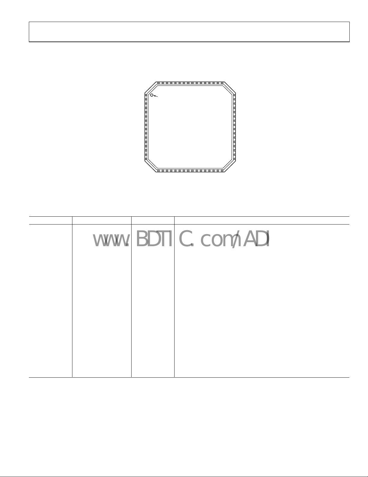
Package: 64-lead LFCSP
APPLICATIONS
1×, 2×, 4× FibreChannel
XAUI
Gigabit Ethernet over backplane
10GBase-CX4
InfiniBand®
50 Ω cables
GENERAL DESCRIPTION
The ADN4600 is an asynchronous, nonblocking crosspoint
switch with eight differential PECL-/CML-compatible inputs
with programmable equalization and eight differential CML
outputs with programmable output levels and pre-emphasis or
de-emphasis. The operation of this device is optimized for NRZ
data at rates up to 4.25 Gbps.
The receive inputs provide programmable equalization with
nine settings to compensate for up to 30 in. of FR4 and
programmable pre-emphasis with seven settings to compensate
for up to 30 in. of FR4 at 4.25 Gbps.
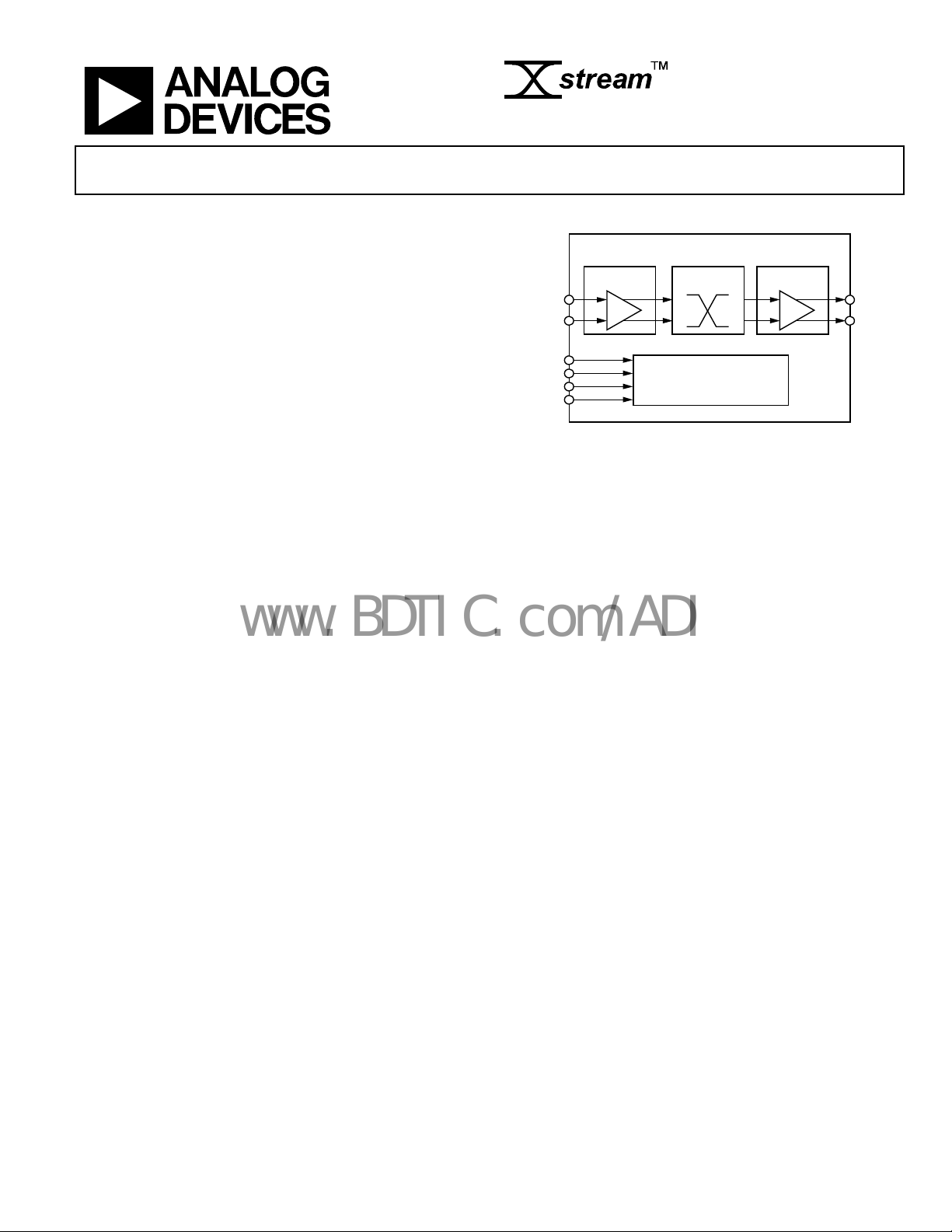
Asynchronous Cross
oint Switch
ADN4600
FUNCTIONAL BLOCK DIAGRAM
ADN4600
RECEIVE
IP[7:0]
IN[7:0]
DDR[1:0]
RESETB
EQUALIZATION
EQ PE
SCL
SDA
The ADN4600 nonblocking switch core implements an 8 × 8
crossbar and supports independent channel switching through the
2
I
C control interface. Every channel implements an asynchronous
path supporting NRZ data rates from dc to 4.25 Gbps. Each
channel is fully independent of other channels. The ADN4600
has low latency and very low channel-to-channel skew.
The main application for the ADN4600 is to support switching
on the backplane, line card, or cable interface sides of serial links.
The ADN4600 is packaged in a 9 mm × 9 mm, 64-lead LFCSP
package and operates from −40°C to +85°C.
CROSSPOINT
ARRAY
CONTROL LOG IC
Figure 1.
TRANSMIT
PRE-EMPHASIS
OP[7:0]
ON[7:0]
07061-001
Rev. 0
Information furnished by Analog Devices is believed to be accurate and reliable. However, no
responsibility is assumed by Analog Devices for its use, nor for any infringements of patents or other
rights of third parties that may result from its use. Specifications subject to change without notice. No
license is granted by implication or otherwise under any patent or patent rights of Analog Devices.
Trademarks and registered trademarks are the property of their respective owners.
One Technology Way, P.O. Box 9106, Norwood, MA 02062-9106, U.S.A.
Tel: 781.329.4700 www.analog.com
Fax: 781.461.3113 ©2008 Analog Devices, Inc. All rights reserved.

ADN4600
www.BDTIC.com/ADI
TABLE OF CONTENTS
Features .............................................................................................. 1
Applications ....................................................................................... 1
Functional Block Diagram .............................................................. 1
General Description ......................................................................... 1
Revision History ............................................................................... 2
Specifications ..................................................................................... 3
Electrical Specifications ............................................................... 3
Timing Specifications .................................................................. 5
Absolute Maximum Ratings ............................................................ 6
ESD Caution .................................................................................. 6
Pin Configuration and Function Descriptions ............................. 7
REVISION HISTORY
6/08—Revision 0: Initial Version
Typical Performance Characteristics ..............................................8
Theory of Operation ...................................................................... 13
Introduction ................................................................................ 13
Receivers ...................................................................................... 13
Switch Core ................................................................................. 15
Transmitters ................................................................................ 16
I2C Control Interface .................................................................. 22
PCB Design Guidelines ............................................................. 24
Control Register Map ..................................................................... 25
Package Outline Dimensions ........................................................ 28
Ordering Guide .......................................................................... 28
Rev. 0 | Page 2 of 2
ADN4600
www.BDTIC.com/ADI
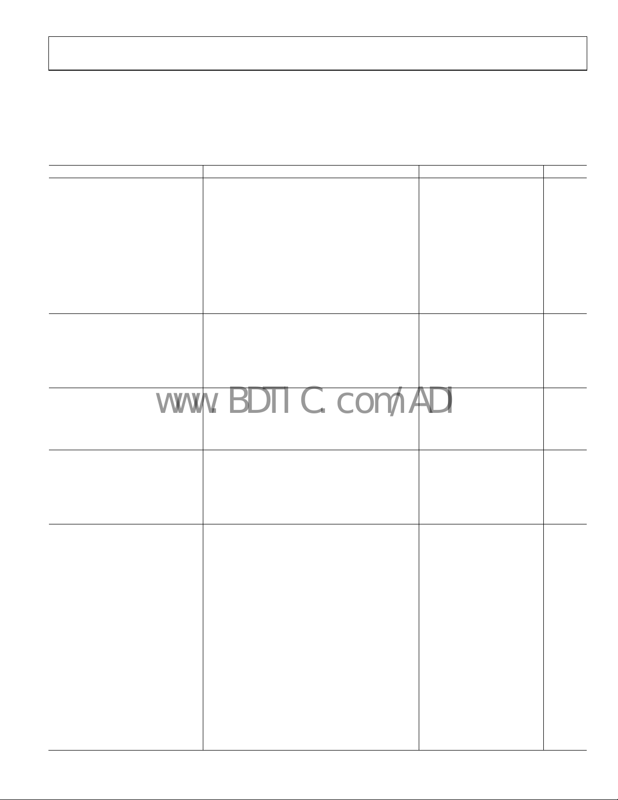
SPECIFICATIONS
ELECTRICAL SPECIFICATIONS
VCC = 1.8 V, VEE = 0 V, V
T
= 25°C, unless otherwise noted.
A
Table 1.
Parameter Conditions Min Typ Max Unit
DYNAMIC PERFORMANCE
Maximum Data Rate per Channel In NRZ format 4.25 Gbps
Deterministic Jitter Data rate < 4.25 Gbps; BER = 1e − 12 30 ps p-p
Random Jitter VCC = 1.8 V 1.5 ps rms
Residual Deterministic Jitter with
Receive Equalization
Residual Deterministic Jitter with
Transmit Pre-Emphasis
Output Rise/Fall Time 20% to 80% 75 ps
Channel-to-Channel Skew 50 ps
Propagation Delay 1 ns
OUTPUT PRE-EMPHASIS
Equalization Method One-tap programmable pre-emphasis
Maximum Boost 800 mV p-p output swing 6 dB
Pre-Emphasis Tap Range Minimum 2 mA
Maximum 12 mA
INPUT EQUALIZATION
Minimum Boost EQBY = 1 1.5 dB
Maximum Boost Maximum boost occurs @ 2.125 GHz 22 dB
Number of Equalization Steps 8 Steps
Gain Step Size 2.5 dB
INPUT CHARACTERISTICS
Input Voltage Swing Differential, V
Input Voltage Range Single-ended absolute voltage level, VL minimum VEE + 0.4 V p-p
Single-ended absolute voltage level, VH maximum VCC + 0.5 V p-p
Input Resistance Single-ended 45 50 55 Ω
Input Return Loss Measured at 2.5 GHz 5 dB
OUTPUT CHARACTERISTICS
Output Voltage Swing @ dc, differential, PE = 0, default, VCC = 1.8 V 635 740 870 mV p-p
@ dc, differential, PE = 0, default, VCC = 3.3 V 800 mV p-p
@ dc, differential, PE = 0, min output level2, VCC = 1.8 V 100 mV p-p
@ dc, differential, PE = 0, min output level2, VCC = 3.3 V 100 mV p-p
@ dc, differential, PE = 0, max output level2, VCC = 1.8 V 1300 mV p-p
@ dc, differential, PE = 0, max output level2, VCC = 3.3 V 1800 mV p-p
Output Voltage Range
Output Current Minimum output current per channel 2 mA
Maximum output current per channel, VCC = 1.8 V 21
Output Resistance Single ended 45 50 55 Ω
Output Return Loss Measured at 2.5 GHz 5 dB
TTI
= V
= VCC, RL = 50 , differential output swing = 800 mV p-p differential, 4.25 Gbps, PRBS 27 − 1,
TTO
Data rate < 3.25 Gbps; 0 in. to 30 in. FR4 0.16 UI
Data rate < 4.25 Gbps; 0 in. to 30 in. FR4 0.20 UI
Data rate < 3.25 Gbps; 0 in. to 30 in. FR4 0.13 UI
Data rate < 4.25 Gbps; 0 in. to 30 in. FR4 0.18 UI
200 mV p-p output swing 12 dB
1
= VCC − 0.6 V; VCC = 3.3 V 300 2000 mV p-p
ICM
Single-ended absolute voltage level,
TxHeadroom = 0; V
Single-ended absolute voltage level,
TxHeadroom = 0; V
Single-ended absolute voltage level,
TxHeadroom = 1; V
Single-ended absolute voltage level,
TxHeadroom = 1; V
min
L
max
H
min
L
max
H
Rev. 0 | Page 3 of 3
V
V
V
V
− 1.1 V
CC
+ 0.6 V
CC
− 1.2 V
CC
+ 0.6 V
CC
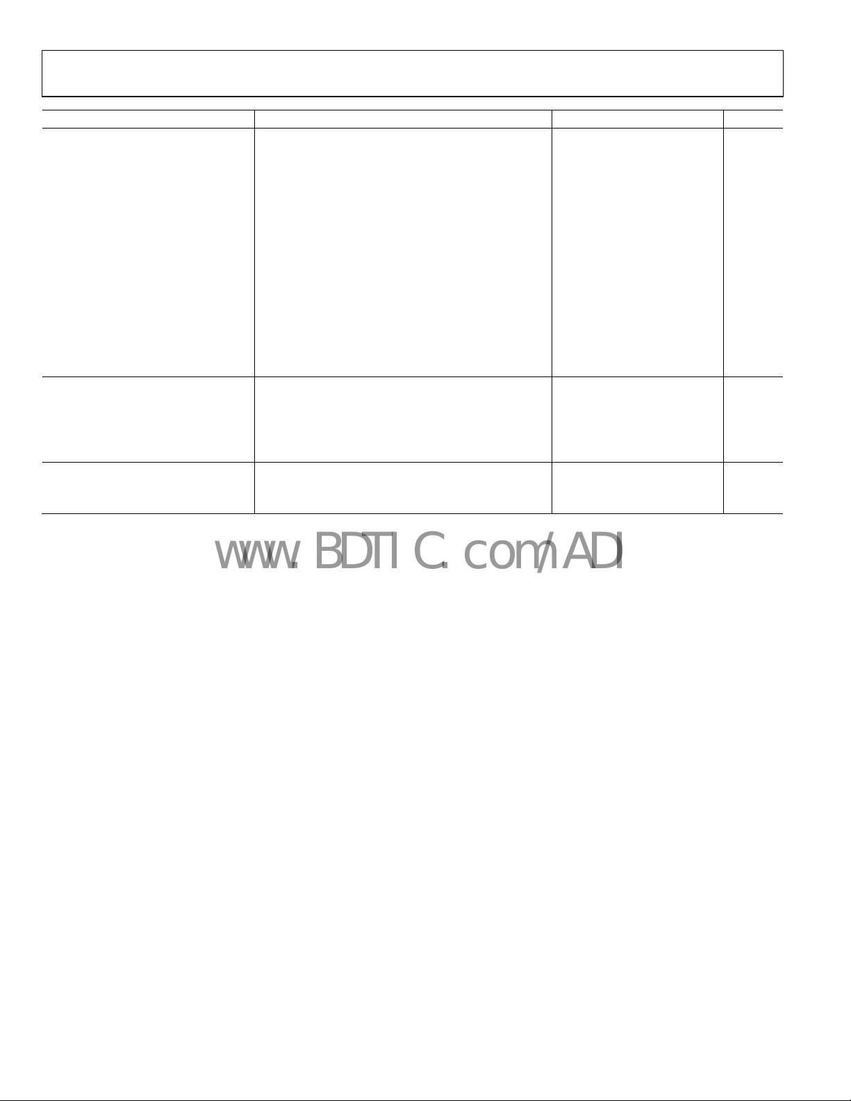
ADN4600
www.BDTIC.com/ADI
Parameter Conditions Min Typ Max Unit
POWER SUPPLY
Operating Range
VCC V
DVCC V
V
(VEE + 0.4 V + 0.5 × VID) < V
TTI
V
(VCC − 1.1 V + 0.5 × VOD) < V
TTO
Supply Current
I
All outputs enabled 63 69 mA
TTO
3
ICC All outputs enabled 460 565 mA
I
EE
I
TTO
ICC Single channel enabled 173 214 mA
IEE Single channel enabled 205 mA
LOGIC CHARACTERISTICS
Input High (VIH) DVCC = 3.3 V 2.5 V
Input Low (VIL) 1.0 V
Output High (VOH) 2.5 V
Output Low (VOL) 1.0 V
THERMAL CHARACTERISTICS
Operating Temperature Range −40 +85 °C
θJA 22 °C/W
1
V
is the input common-mode voltage.
ICM
2
Programmable via I2C.
3
Assumes dc-coupled outputs. For ac-coupled outputs, I
= 0 V 1.7 1.8 3.6 V
EE
= 0 V, DVCC ≤ (VCC + 1.3 V) 3.0 3.3 3.6 V
EE
< (VCC + 0.5 V)
TTI
V
EE
1.8 3.6 V
+
0.4
< (VCC + 0.5 V)
TTO
V
CC
1.8 3.6 V
−
1.1
All outputs enabled 586 mA
Single channel enabled 16 18 mA
currents will double.
TTO
Rev. 0 | Page 4 of 4
ADN4600
www.BDTIC.com/ADI
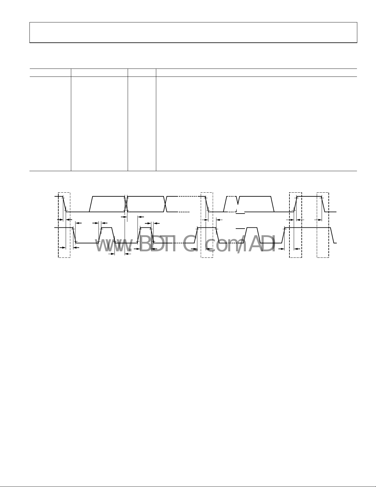
TIMING SPECIFICATIONS
Table 2. I2C Timing Parameters
Parameter Min Max Unit Description
f
0 400 kHz SCL clock frequency
SCL
t
0.6 N/A
HD;STA
t
0.6 N/A
SU;STA
t
1.3 N/A
LOW
t
0.6 N/A
HIGH
t
0 N/A
HD;DAT
t
10 N/A ns Data setup time
SU;DAT
μs
μs
μs
μs
μs
tr 1 300 ns Rise time for both SDA and SCL
tf 1 300 ns Fall time for both SDA and SCL
t
0.6 N/A
SU;STO
t
1 N/A ns Bus-free time between a stop and a start condition
BUF
μs
CIO 5 7 Pf Capacitance for each I/O pin
I2C Timing Specifications
SDA
Hold time for a start condition
Setup time for a repeated start condition
Low period of the SCL clock
High period of the SCL clock
Data hold time
Setup time for a stop condition
t
t
HD:DAT
SU:DAT
t
f
t
HIGH
t
f
Figure 2. I
t
SU:STA
2
C Timing Diagram
t
HD:STA
t
SU:STO
t
f
t
BUF
SPSrS
07061-010
SCL
t
f
t
LOW
t
HD:STA
Rev. 0 | Page 5 of 5

ADN4600
www.BDTIC.com/ADI
ABSOLUTE MAXIMUM RATINGS
Table 3.
Parameter Rating
VCC to VEE 3.7 V
V
V
TTI
V
V
TTO
Internal Power Dissipation
Differential Input Voltage 2.0 V
Logic Input Voltage VEE − 0.3 V < VIN < VCC + 0.6 V
Storage Temperature Range −65°C to +125°C
Lead Temperature 300°C
+ 0.6 V
CC
+ 0.6 V
CC
4.26 W
Stresses above those listed under Absolute Maximum Ratings
may cause permanent damage to the device. This is a stress
rating only; functional operation of the device at these or any
other conditions above those indicated in the operational
section of this specification is not implied. Exposure to absolute
maximum rating conditions for extended periods may affect
device reliability.
ESD CAUTION
Rev. 0 | Page 6 of 6
ADN4600
www.BDTIC.com/ADI
PIN CONFIGURATION AND FUNCTION DESCRIPTIONS
VEE
VCC
VEE
OP0
ON0
VCC
OP1
ON1
VTTO
OP2
ON2
VEE
OP3
ON3
ADDR1
646362616059585756555453525150
ADDR0
49
RESETB
VEE
IN0
IP0
VCC
IN1
IP1
VTTI
IN2
IP2
10
VEE
11
IN3
12
IP3
13
DVCC
14
VCC
15
VEE
16
NOTES
1. PAD ON BOT TOM OF PACKAGE MUST BE CONNECTED TO VEE.
PIN 1
1
INDICATOR
2
3
4
5
6
7
8
9
171819202122232425262728293031
VEE
VCC
OP7
ON7
ADN4600
TOP VIEW
(Not to Scale)
OP6
ON6
VCC
VTTO
OP5
VEE
OP4
ON5
VEE
ON4
48
SCL
47
SDA
46
VEE
45
IP7
44
IN7
43
VCC
42
IP6
41
IN6
40
VTTI
39
IP5
38
IN5
37
VEE
36
IP4
35
IN4
34
VCC
33
VEE
32
VEE
VCC
07061-002
Figure 3. Pin Configuration
Table 4. Pin Function Descriptions
Pin No. Mnemonic Type Description
1 RESETB Control Reset Input (Active Low)
2, 11, 16, 17, 27,
VEE Power Negative Supply
30, 32, 33, 37,
46, 53, 62, 64
3, 6, 9, 12, 35,
IN0 to IN7 I/O High Speed Inputs
38, 41, 44
4, 7, 10, 13, 36,
IP0 to IP7 I/O High Speed Input Complements
39, 42, 45
5, 15, 18, 21, 31,
VCC Power Positive Supply
34, 43, 59, 63
8, 40 VTTI Power Input Termination Supply
14 DVCC Power Digital Positive Supply (3.3 V)
19, 22, 25, 28,
ON7 to ON0 I/O High Speed Outputs
51, 54, 57, 60
20, 23, 26, 29,
OP7 to ON0 I/O High Speed Output Complements
52, 55, 58, 61
24, 56 VTTO Power Output Termination Supply
47 SDA Control I2C Control Interface Data Input/Output
48 SCL Control I2C Control Interface Clock Input
49 ADDR0 Control I2C Control Interface Address LSB
50 ADDR1 Control I2C Control Interface Address MSB
EPAD Power Connect to VEE
Rev. 0 | Page 7 of 7
ADN4600
V
V
V
V
www.BDTIC.com/ADI
TYPICAL PERFORMANCE CHARACTERISTICS
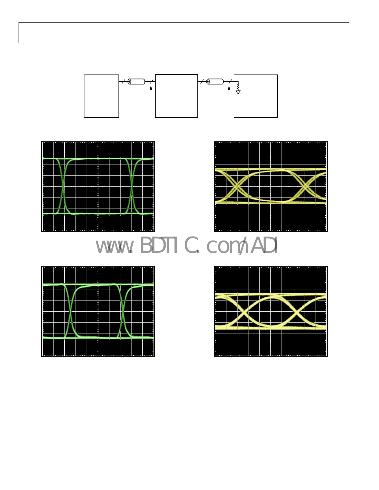
Figure 5 to Figure 8 were obtained using the standard test circuit shown in Figure 4.
DATA OUT
PATTERN
GENERATOR
2 2
INPUT
PIN
ADN4600
AC-COUPL ED
EVALUATION
OUTPUT
BOARD
50Ω CABLES
Figure 4. Standard Test Circuit (No Channel)
50Ω CABLES
2 2
PIN
50Ω
TP2TP1
OSCILLOSCOPE
HIGH SPEED
SAMPLING
07061-011
200mV/DI
50ps/DIV
07061-012
Figure 5. 3.25 Gbps Input Eye
(TP1 from Figure 4)
200mV/DI
50ps/DIV
07061-013
Figure 6. 4.25 Gbps Input Eye
(TP1 from Figure 4)
200mV/DI
50ps/DIV
Figure 7. 3.25 Gbps Output Eye, No Channel
(TP2 from Figure 4)
200mV/DI
50ps/DIV
Figure 8. 4.25 Gbps Output Eye, No Channel
(TP2 from Figure 4)
07061-014
07061-015
Rev. 0 | Page 8 of 8
ADN4600
V
V
V
V
www.BDTIC.com/ADI
Figure 10 to Figure 13 were obtained using the standard test circuit shown in Figure 9.
DATA OUT
PATTERN
GENERATOR
50Ω CABLES
2 2
FR4 TEST BACKPLANE
DIFFERENTIAL
STRIPLINE TRACES
TP1
8mils WIDE, 8mils SPACE,
8mils DIELECTRIC HEIGHT
TRACE LENGTHS = 30''
50Ω CABLES
2 2
TP2
INPUT
OUTPUT
PIN
ADN4600
AC-COUPLED
EVALUATION
BOARD
Figure 9. Input Equalization Test Circuit, FR4 (See Figure 5 and Figure 6 for the Reference Eye Diagrams at TP1)
2 2
PIN
50Ω CABLES
50Ω
HIGH SPEED
TP3
SAMPLING
OSCILLOSCOPE
07061-016
200mV/DI
50ps/DIV
Figure 10. 3.25 Gbps Input Eye, 30 Inch FR4 Input Channel
(TP2 from Figure 9)
200mV/DI
50ps/DIV
Figure 11. 4.25 Gbps Input Eye, 30 Inch FR4 Input Channel
(TP2 from Figure 9)
200mV/DI
07061-017
50ps/DIV
07061-019
Figure 12. 3.25 Gbps Output Eye, 30 Inch FR4 Input Channel, Best EQ Setting
(TP3 from Figure 9)
200mV/DI
07061-018
50ps/DIV
07061-020
Figure 13. 4.25 Gbps Output Eye, 30 Inch FR4 Input Channel, Best EQ Setting
(TP3 from Figure 9)
Rev. 0 | Page 9 of 9

ADN4600
V
V
V
V
www.BDTIC.com/ADI
Figure 15 to Figure 18 were obtained using the standard test circuit shown in Figure 14.
DATA OUT
PATTERN
GENERATOR
50Ω CABLES
2 2
TP1
INPUT
OUTPUT
PIN
ADN4600
AC-COUPLED
EVALUATIO N
BOARD
50Ω CABLES
2 2
PIN
FR4 TEST BACKPLANE
DIFFERENTIAL
STRIPLINE TRACES
TP2
8mils WIDE, 8mils SPACE,
8mils DIELECTRIC HEIGHT
TRACE LENGT HS = 30''
Figure 14. Output Pre-Emphasis Test Circuit, FR4
50Ω CABLES
2 2
TP3
50Ω
HIGH SPEED
SAMPLING
OSCILLOSCOPE
07061-021
200mV/DI
50ps/DIV
Figure 15. 3.25 Gbps Output Eye, 30 Inch FR4 Output Channel, PE = 0
(TP3 from Figure 14)
200mV/DI
50ps/DIV
Figure 16. 4.25 Gbps Output Eye, 30 Inch FR4 Output Channel, PE = 0
(TP3 from Figure 14)
200mV/DI
07061-022
50ps/DIV
07061-024
Figure 17. 3.25 Gbps Output Eye, 30 Inch FR4 Output Channel, PE = Best Setting
(TP3 from Figure 14)
200mV/DI
07061-023
50ps/DIV
07061-025
Figure 18. 4.25 Gbps Output Eye, 30 Inch FR4 Output Channel, PE = Best Setting
(TP3 from Figure 14)
Rev. 0 | Page 10 of 10

ADN4600
www.BDTIC.com/ADI
Test conditions: VCC = 1.8 V, VEE = 0 V, V
unless otherwise noted.
80
70
60
TTI
= V
= VCC, RL = 50 , differential output swing = 800 mV p-p differential, TA = 25°C,
TTO
100
80
50
40
30
20
DETERMINISTIC JITTER (ps)
10
0
02040
DATA RATE (Hz)
Figure 19. Deterministic Jitter vs. Data Rate
100
90
80
70
60
50
40
30
DETERMINISTIC JITTER (ps)
20
10
0
0 0.5 1.0 1.5 2.0 2.5
DIFFERENTIAL INPUT SWING (V)
Figure 20. Deterministic Jitter vs. Input Swing
60
07061-026
07061-027
60
40
DETERMINI STIC JIT TER (ps)
20
0
1.0 1.5 2.0 2.5 3.0 3.5 4.0
VCC = 1.8V
VCC = 3.3V
INPUT COMMON MODE (V)
Figure 22. Deterministic Jitter vs. Input Common Mode
100
80
60
40
DETERMINI STIC JIT TER (ps)
20
0
1.0 1.5 2.0 2.5 3.0 3.5 4.0
(V)
V
CC
Figure 23. Deterministic Jitter vs. Supply Voltage
07061-029
07061-030
100
80
60
40
DETERMINI STIC JIT TER (ps)
20
0
–60 –40 –20 0 20 40 60 80 100
TEMPERATURE ( °C)
07061-028
Figure 21. Deterministic Jitter vs. Temperature
Rev. 0 | Page 11 of 11
100
80
60
40
DETERMINI STIC JIT TER (ps)
20
0
1.0 1.5 2.0 2.5 3.0 3.5 4.0
V
TTO
VCC = 1.8V
VCC = 3.3V
(V)
Figure 24. Deterministic Jitter vs. Output Termination Voltage
07061-031

ADN4600
www.BDTIC.com/ADI
450000
400000
350000
300000
250000
200000
150000
NUMBER OF SAMPLES
100000
50000
0
–8 –6 –4 –2 0 2 4 6 8 10
JITTER ( ps)
07061-032
Figure 25. Random Jitter Histogram
100
90
80
(ps)
F
/t
R
t
70
60
50
–60 –40 –20 0 20 40 60 80 100
tR/t
F
TEMPERATURE ( °C)
Figure 26. Rise Time/Fall Time vs. Temperature
07061-033
Rev. 0 | Page 12 of 12

ADN4600
A
www.BDTIC.com/ADI
THEORY OF OPERATION
INTRODUCTION
The ADN4600 is an 8 × 8, buffered, asynchronous, 8-channel
crosspoint switch that allows fully nonblocking connectivity
between its transmitters and receivers. The switch supports
multicast and broadcast operation, allowing the ADN4600 to
work in redundancy and port-replication applications.
ADN4600
IP[7:0]
IN[7:0]
DDR[1:0]
SCL
SDA
RESETB
RECEIVE
EQUALIZATION
EQ PE
Figure 27. Simplified Functional Block Diagram
CROSSPOINT
ARRAY
CONTROL LOG IC
TRANSMIT
PRE-EMPHASIS
OP[7:0]
ON[7:0]
The ADN4600 offers extensively programmable output levels
and pre-emphasis, as well as a squelch function and the ability
to fully disable the device. The receivers integrate a programmable,
multizero transfer function that has been optimized to compensate
either typical backplane or typical cable losses. The ADN4600
provides a balanced, high speed switch core that maintains low
channel-to-channel skew and preserves edge rates.
The I/O on-chip termination resistors are tied to user-settable
supplies to support dc coupling in various logic styles. The
ADN4600 supports a wide core supply range; V
can be set
CC
from 1.8 V to 3.3 V. These features together with programmable
transmitter output levels allow for several dc- and ac-coupled
I/O configurations.
RECEIVERS
Input Structure and Input Levels
VCC
VTTI
IPx
INx
VEE
The ADN4600 receiver inputs incorporate 50 termination
resistors, ESD protection, and a multizero transfer function
equalizer that can be optimized for backplane and cable operation.
Each receive channel also provides a positive/negative (P/N)
SIMPLIFIED RECEIVER INPUT CIRCUIT
RLN
RP
52Ω
Figure 28. Simplified Input Structure
RN
52Ω
R1
750Ω
R2
750Ω
R3
1kΩ
Q1
Q2
RLP
RL
I1
RL
7061-003
07061-004
inversion function, which allows the user to swap the sign of the
input signal path to eliminate the need for board-level
crossovers in the receiver channel.
Tabl e 5 illustrates some, but not all, possible combinations of
input supply voltages.
Equalization Settings
The ADN4600 receiver incorporates a multizero transfer
function with a continuous time equalizer, providing up to
22 dB of high-frequency boost at 2.25 GHz to compensate for
up to 30 in. of FR4 at 4.25 Gbps. The ADN4600 also allows
independent control of the equalizer transfer function on each
channel through the I
2
C control interface.
In the basic mode of operation, the equalizer transfer function
allows independent control of the boost in two frequency ranges
for optimal matching with the loss shape of the channel (for
example, the shape due primarily to skin effect or to dielectric
loss). The total equalizer shape space is reduced to two independent
frequency response groups—one optimized for cable and the
other optimized for FR4 material. The RX EQ bits of the
RX[7:0] configuration registers provide eight settings for each
frequency response group to ease programming for typical
channels.
Tabl e 6 summarizes the high-frequency boost for the frequency
response grouping optimized for the FR4 material; it lists the basic
control settings and the typical length of FR4 trace compensated
for by each setting. All eight channels of the ADN4600 use the
FR4-optimized frequency response grouping by default. The
user can override this default by setting the respective RX LUT
select bit high and then selecting the frequency response grouping
by setting the RX LUT FR4/CX4 bit high for FR4 and low for
cable. Setting the RX EQBY bit of the RX[7:0] configuration
registers high sets the equalization to 1.5 dB of boost, which
compensates for 0 m to 2 m of CX4 or 0 in. to 10 in. of FR4.
In the advanced mode of operation, full control of the equalizer is
available through the I
2
C control interface. The user can specify
the boost in the midfrequency range and the boost in the high
frequency range independently. This is accomplished by
circumventing the frequency response groupings shown in
Tabl e 6 by setting the EQ CTL SRC bit (Bit 6 of the RX[7:0]
EQ1 control registers) high and writing directly to the equalizer
control bits on a per channel basis. Therefore, write values to
Bits[5:0] of the RX[7:0] EQ1 control registers and to Bits[5:0]
of the RX[7:0] EQ3 control registers for the channel of interest.
The bits of these registers are ordered such that Bit 5 is a sign
bit, and midlevel boost is centered around 0x00. Setting Bit 5
low and increasing the LSBs decreases the boost, whereas
setting Bit 5 high and increasing the LSBs increases the boost.
Rev. 0 | Page 13 of 13

ADN4600
www.BDTIC.com/ADI
Table 5. Common Input Voltage Levels
Configuration VCC (V) V
Low V
, AC-Coupled Input 1.8 1.6
TTI
Single 1.8 V Supply 1.8 1.8
3.3 V Core 3.3 1.8
Single 3.3 V Supply 3.3 3.3
Table 6. Receive Equalizer Boost vs. Setting
RX EQ Bit Settings Boost (dB) Typical FR4 Trace Length (Inches)
0 3.5 5 to 10
1 3.9 10 to 15
2 4.25 15 to 20
3 4.5 20 to 25
4 4.75 25 to 30
5 5.0 30 to 35
6 5.3 35 to 40
7 5.5 35 to 40
Table 7. Equalization Control Registers
Name Addr Bit 7 Bit 6 Bit 5 Bit 4 Bit 3 Bit 2 Bit 1 Bit 0 Default
RX[7:0] Configuration 0xB8, 0xB0,
0xA8, 0xA0,
0x98, 0x90,
0x88, 0x80
RX[7:0] EQ1 Control 0xBB, 0xB3,
0xAB, 0xA3,
0x9B, 0x93,
0x8B, 0x83
RX[7:0] EQ3 Control 0xBC, 0xB4,
0xAC, 0xA4,
0x9C, 0x94,
0x8C, 0x84
RX[7:0] FR4 Control 0xBD, 0xB5,
0xAD, 0xA5,
0x9D, 0x95,
0x8D, 0x85
RX PNSWAP RX EQBY RX EN RX EQ[2] RX EQ[1] RX EQ[0] 0x30
EQ CTL SRC RX EQ1[5] RX EQ1[4] RX EQ1[3] RX EQ1[2] RX EQ1[1] RX EQ1[0] 0x00
RX EQ3[5]
RX LUT
RX EQ3[4] RX EQ3[3] RX EQ3[2] RX EQ3[1] RX EQ3[0] 0x00
select
Lane Inversion
The receiver P/N inversion feature is a convenience intended to
allow the user to implement the equivalent of a board-level
crossover in a much smaller area and without additional via
impedance discontinuities that degrade the high-frequency
integrity of the signal path. The P/N inversion is independent
for each of the eight channels and is controlled through the I
control interface.
Wa r ni n g
Using the lane inversion feature to account for signal inversions
downstream of the receiver requires additional attention when
switching connectivity.
(V)
TTI
RX LUT
FR4/CX4
0x00
2
C
Rev. 0 | Page 14 of 14

ADN4600
www.BDTIC.com/ADI
SWITCH CORE
The ADN4600 switch core is a fully nonblocking 8 × 8 array
that allows multicast and broadcast configurations. The
configuration of the switch core is controlled through the I
control interface. The control interface receives and stores the
desired connection matrix for the eight input and eight output
signal pairs. The interface consists of eight rows of double-rank
latches, one for each output. The 2-bit data-word stored in these
latches indicates to which (if any) of the eight inputs the output
will be connected.
One output at a time can be preprogrammed by addressing the
output and writing the desired connection data into the first rank
of latches. This is done by writing to the XPT configuration
register (Address 0x40). The output being addressed is written
into Bits[2:0], and the input being sent to this output is written
into Bits[6:4]. This process can be repeated until each of the
Table 8. Switch Core Control and Status Registers
Name Addr Bit 7 Bit 6 Bit 5 Bit 4 Bit 3 Bit 2 Bit 1 Bit 0 Default
XPT Configuration 0x40
XPT Update 0x41 Update 0x00
XPT Status 0 0x50 OUT0[2] OUT0[1] OUT0[0] N/A
XPT Status 1 0x51 OUT1[2] OUT1[1] OUT1[0] N/A
XPT Status 2 0x52 OUT2[2] OUT2[1] OUT2[0] N/A
XPT Status 3 0x53 OUT3[2] OUT3[1] OUT3[0] N/A
XPT Status 4 0x54 OUT4[2] OUT4[1] OUT4[0] N/A
XPT Status 5 0x55 OUT5[2] OUT5[1] OUT5[0] N/A
XPT Status 6 0x56 OUT6[2] OUT6[1] OUT6[0] N/A
XPT Status 7 0x57 OUT7[2] OUT7[1] OUT7[0] N/A
IN PORT
[2]
IN PORT
[1]
2
C
IN PORT
[0]
desired output changes has been preprogrammed. Bit 3 of the
XPT configuration register (Address 0x40) signals whether a
broadcast condition is desired. If this bit is set high, the input
selected by Bits[6:4] is sent to all outputs. All output connections
can then be programmed simultaneously by passing the data
from the first rank of latches into the second rank by writing
0x01 to the XPT update register (Address 0x41). This is a selfclearing register and therefore always reads back as 0x00. The
output connections always reflect the data programmed into the
second rank of latches and do not change until the first rank of data
is passed into the second rank by strobing the XPT update register.
If necessary for system verification, the data in the first rank of
latches can be read back from the control interface. This is done
by reading from the XPT Temp[3:0] registers, which show the
status of the input data programmed in the first rank of latches
for each output.
Broadcast
OUT PORT
[2]
OUT PORT
[1]
OUT PORT
[0]
0x00
Table 9. Switch Core Temporary Registers
Name Addr Bit 7 Bit 6 Bit 5 Bit 4 Bit 3 Bit 2 Bit 1 Bit 0 Default
XPT Temp 0 0x58 OUT1[2] OUT1[1] OUT1[0] OUT0[2] OUT0[1] OUT0[0] N/A
XPT Temp 1 0x59 OUT3[2] OUT3[1] OUT3[0] OUT2[2] OUT2[1] OUT2[0] N/A
XPT Temp 2 0x5A OUT5[2] OUT5[1] OUT5[0] OUT4[2] OUT4[1] OUT4[0] N/A
XPT Temp 3 0x5B OUT7[2] OUT7[1] OUT7[0] OUT6[2] OUT6[1] OUT6[0] N/A
Rev. 0 | Page 15 of 15

ADN4600
www.BDTIC.com/ADI
TRANSMITTERS
Output Structure and Output Levels
The ADN4600 transmitter outputs incorporate 50 termination
resistors, ESD protection, and output current switch. Each
channel provides independent control of both the absolute
output level and the pre-emphasis output level. It should be
noted that the choice of output level affects the output commonmode level. A 600 mV p-p differential output level with full
pre-emphasis range requires an output termination voltage
of 2.5 V or greater; therefore, for the VTTO pin, V
equal to or greater than 2.5 V.
Pre-Emphasis
The total output amplitude and pre-emphasis setting space is
reduced to a single map of basic settings that provides seven
settings of output equalization to ease programming for typical
channels. The full resolution of seven settings is available through
2
the I
C interface by writing to Bits[2:0] (the TX PE[2:0] bits) of
the TX[7:0] configuration registers. Tabl e 10 summarizes the
absolute output level, pre-emphasis level, and high frequency
boost for each of the control settings and the typical length of
FR4 trace compensated for by each setting.
Full control of the transmit output levels is available through the
2
I
C control interface. This full control is achieved by writing to
the TX[7:0] Output Level Control[1:0] registers for the channel
of interest. The supported output levels are shown in Ta bl e 1 2 .
The TX[7:0] Output Level Control[1:0] registers must be
programmed to one of the supported settings listed in this table;
other settings are not supported.
must be
CC
The output equalization is optimized for less than 2.5 Gbps
operation, but can be optimized for higher speed applications
up to 4.25 Gbps through the I
2
C control interface by writing to
the TX DATA RATE bit (Bit 4) of the TX[7:0] configuration
register, with high representing 4.25 Gbps and low representing
2.5 Gbps. The TX[7:0] CTL SRC bit (Bit 7) in the TX[7:0]
Output Level Control 1 register determines whether the preemphasis and output current controls for the channel of interest
are selected from the optimized map or directly from the
TX[7:0] Output Level Control[1:0] registers (per channel).
Setting this bit high selects pre-emphasis control directly from
the TX[7:0] Output Level Control[1:0] registers, and setting it
low selects pre-emphasis control from the optimized map.
TX SIMPL IFIED DI AGRAM
V3
VC
V2
VP
V1
VN
I
+ T
DC
Figure 29. Simplified Output Structure
ON-CHIP
TERMINATI ON
RP
52Ω
Q1
Q2
IT
PE
RN
52Ω
ESD
VCC
VTTO
OPx
ONx
VEE
07061-006
Table 10. Transmit Pre-Emphasis Boost and Overshoot vs. Setting
TX PE Boost (dB) Overshoot DC Swing (mV p-p Differential) Typical FR4 Trace Length (Inches)
0 0 0% 800 0 to 5
1 2 25% 800 0 to 5
2 3.5 50% 800 10 to 15
3 4.9 75% 800 15 to 20
4 6 100% 800 25 to 30
5 7.4 133% 600 30 to 35
6 9.5 200% 400 35 to 40
Table 11. Transmitters Control Registers
Name Addr Bit 7 Bit 6 Bit 5 Bit 4 Bit 3 Bit 2 Bit 1 Bit 0 Def.
TX[7:0]
Configuration
TX[7:0] Output
Level Control 1
TX[7:0] Output
Level Control 0
0xE0, 0xE8,
0xF0, 0xF8,
0xD8, 0xD0,
0xC8, 0xC0
0xE1, 0xE9,
0xF1, 0xF9,
0xD9, 0xD1,
0xC9, 0xC1
0xE2, 0xEA,
0xF2, 0xFA,
0xDA, 0xD2,
0xCA, 0xC2
TX EN TX data
rate
TX[7:0]
CTL SRC
TX[7:0]_OLEV0[6:0] 0x40
TX PE[2] TX PE[1] TX PE[0] 0x20
TX[7:0]_OLEV1[6:0] 0x40
Rev. 0 | Page 16 of 16

ADN4600
www.BDTIC.com/ADI
Table 12. Output Level Programming
VOD (mV) VD Peak (mV) PE (dB) I
50 50 0.00 2 0x00 0x81
50 150 9.54 6 0x11 0x81
50 250 13.98 10 0x22 0x81
50 350 16.90 14 0x33 0x81
50 450 19.08 18 0x44 0x81
50 550 20.83 22 0x55 0x81
50 650 22.28 26 0x66 0x81
100 100 0.00 4 0x00 0x91
100 200 6.02 8 0x11 0x91
100 300 9.54 12 0x22 0x91
100 400 12.04 16 0x33 0x91
100 500 13.98 20 0x44 0x91
100 600 15.56 24 0x55 0x91
100 700 16.90 28 0x66 0x91
150 150 0.00 6 0x00 0x92
150 250 4.44 10 0x11 0x92
150 350 7.36 14 0x22 0x92
150 450 9.54 18 0x33 0x92
150 550 11.29 22 0x44 0x92
150 650 12.74 26 0x55 0x92
150 750 13.98 30 0x66 0x92
200 200 0.00 8 0x00 0xA2
200 300 3.52 12 0x11 0xA2
200 400 6.02 16 0x22 0xA2
200 500 7.96 20 0x33 0xA2
200 600 9.54 24 0x44 0xA2
200 700 10.88 28 0x55 0xA2
200 800 12.04 32 0x66 0xA2
250 250 0.00 10 0x00 0xA3
250 350 2.92 14 0x11 0xA3
250 450 5.11 18 0x22 0xA3
250 550 6.85 22 0x33 0xA3
250 650 8.30 26 0x44 0xA3
250 750 9.54 30 0x55 0xA3
250 850 10.63 34 0x66 0xA3
300 300 0.00 12 0x00 0xB3
300 400 2.50 16 0x11 0xB3
300 500 4.44 20 0x22 0xB3
300 600 6.02 24 0x33 0xB3
300 700 7.36 28 0x44 0xB3
300 800 8.52 32 0x55 0xB3
300 900 9.54 36 0x66 0xB3
350 350 0.00 14 0x00 0xB4
350 450 2.18 18 0x11 0xB4
350 550 3.93 22 0x22 0xB4
350 650 5.38 26 0x33 0xB4
350 750 6.62 30 0x44 0xB4
350 850 7.71 34 0x55 0xB4
350 950 8.67 38 0x66 0xB4
400 400 0.00 16 0x00 0xC4
400 500 1.94 20 0x11 0xC4
400 600 3.52 24 0x22 0xC4
(mA) Tx[7:0] Output Level Control 0 Tx[7:0] Output Level Control 1
TOT
Rev. 0 | Page 17 of 17

ADN4600
www.BDTIC.com/ADI
VOD (mV) VD Peak (mV) PE (dB) I
400 700 4.86 28 0x33 0xC4
400 800 6.02 32 0x44 0xC4
400 900 7.04 36 0x55 0xC4
400 1000 7.96 40 0x66 0xC4
450 450 0.00 18 0x00 0xC5
450 550 1.74 22 0x11 0xC5
450 650 3.19 26 0x22 0xC5
450 750 4.44 30 0x33 0xC5
450 850 5.52 34 0x44 0xC5
450 950 6.49 38 0x55 0xC5
450 1050 7.36 42 0x66 0xC5
500 500 0.00 20 0x00 0xD5
500 600 1.58 24 0x11 0xD5
500 700 2.92 28 0x22 0xD5
500 800 4.08 32 0x33 0xD5
500 900 5.11 36 0x44 0xD5
500 1000 6.02 40 0x55 0xD5
500 1100 6.85 44 0x66 0xD5
550 550 0.00 22 0x00 0xD6
550 650 1.45 26 0x11 0xD6
550 750 2.69 30 0x22 0xD6
550 850 3.78 34 0x33 0xD6
550 950 4.75 38 0x44 0xD6
550 1050 5.62 42 0x55 0xD6
550 1150 6.41 46 0x66 0xD6
600 600 0.00 24 0x00 0xE6
600 700 1.34 28 0x11 0xE6
600 800 2.50 32 0x22 0xE6
600 900 3.52 36 0x33 0xE6
600 1000 4.44 40 0x44 0xE6
600 1100 5.26 44 0x55 0xE6
600 1200 6.02 48 0x66 0xE6
650 650 0.00 26 0x01 0xE6
650 750 1.24 30 0x12 0xE6
650 850 2.33 34 0x23 0xE6
650 950 3.30 38 0x34 0xE6
650 1050 4.17 42 0x45 0xE6
650 1150 4.96 46 0x56 0xE6
700 700 0.00 28 0x02 0xE6
700 800 1.16 32 0x13 0xE6
700 900 2.18 36 0x24 0xE6
700 1000 3.10 40 0x35 0xE6
700 1100 3.93 44 0x46 0xE6
750 750 0.00 30 0x03 0xE6
750 850 1.09 34 0x14 0xE6
750 950 2.05 38 0x25 0xE6
750 1050 2.92 42 0x36 0xE6
800 800 0.00 32 0x04 0xE6
800 900 1.02 36 0x15 0xE6
800 1000 1.94 40 0x26 0xE6
850 850 0.00 34 0x05 0xE6
850 950 0.97 38 0x16 0xE6
900 900 0.00 36 0x06 0xE6
(mA) Tx[7:0] Output Level Control 0 Tx[7:0] Output Level Control 1
TOT
Rev. 0 | Page 18 of 18

ADN4600
www.BDTIC.com/ADI
High Current Setting and Output Level Shift
In low voltage applications, users must pay careful attention to
both the differential and common-mode signal levels (see Figure 30
and Tabl e 13 ). Failure to understand the implications of signal
level and choice of ac or dc coupling will almost certainly lead
to transistor saturation and poor transmitter performance.
TxHeadroom
dV
OCM
V
OD
VTTO
V
H
V
OCM
V
L
There is a TxHeadroom register (I2C Register Address 0x23)
V
that allows configuration of the individual transmitters for
extra headroom at the output for high current applications. The
bits in this register are active high (default). There is one bit for
each transmitter of the device (see Ta b le 1 7 ). Setting this bit
= 2 × V
ODPP
Figure 30. Simplified Output Voltage Levels Diagram
OD
VEE
07061-007
high puts the respective transmitter in a configuration for extra
headroom, and setting this bit low does not provide extra
headroom.
Signal Levels and Common-Mode Shift for DC- and AC-Coupled Outputs
Table 13. Signal Levels and Common-Mode Shift for DC- and AC-Coupled Outputs
Output Levels and Output Compliance AC-Coupled Transmitter DC-Coupled Transmitter TxHeadroom = 0 TxHeadroom = 1
VOD
I
TOT
(mV)
(mA)
V
and VCC = 3.3 V
TTO
V
D
Peak
(mV)
PE
Boost
PE
(dB)
dV
OCM
(mV)
VL
V
H
Peak
Peak
VH
VL
(V)
(V)
(V)
(V)
dV
OCM
(mV)
VH
(V)
VL
(V)
V
H
Peak
(V)
VL
Peak
(V)
Min
V
L
(V)
Max
VCC − VL
(V)
200 8 200 1.00 0.00 200 3.2 3 3.2 3 100 3.3 3.1 3.3 3.1 2.225 1.1 1.8 2 1.2 2
200 12 300 1.50 3.52 300 3.1 2.9 3.15 2.85 150 3.25 3.05 3.3 3 2.225 1.1 1.8 2 1.2 2
200 16 400 2.00 6.02 400 3 2.8 3.1 2.7 200 3.2 3 3.3 2.9 2.225 1.1 1.8 2 1.2 2
200 20 500 2.50 7.96 500 2.9 2.7 3.05 2.55 250 3.15 2.95 3.3 2.8 2.225 1.1 1.8 2 1.2 2
200 24 600 3.00 9.54 600 2.8 2.6 3 2.4 300 3.1 2.9 3.3 2.7 2.225 1.1 1.8 2 1.2 2
200 28 700 3.50 10.88 700 2.7 2.5 2.95 2.25 350 3.05 2.85 3.3 2.6 2.225 1.1 1.9 2 1.2 2.2
200 32 800 4.00 12.04 800 2.6 2.4 2.9 2.1 400 3 2.8 3.3 2.5 2.225 1.1 1.9 2 1.2 2.2
300 12 300 1.00 0.00 300 3.15 2.85 3.15 2.85 150 3.3 3 3.3 3 2.225 1.1 1.8 2 1.2 2
300 16 400 1.33 2.50 400 3.05 2.75 3.1 2.7 200 3.25 2.95 3.3 2.9 2.225 1.1 1.8 2 1.2 2
300 20 500 1.67 4.44 500 2.95 2.65 3.05 2.55 250 3.2 2.9 3.3 2.8 2.225 1.1 1.8 2 1.2 2
300 24 600 2.00 6.02 600 2.85 2.55 3 2.4 300 3.15 2.85 3.3 2.7 2.225 1.1 1.8 2 1.2 2
300 28 700 2.33 7.36 700 2.75 2.45 2.95 2.25 350 3.1 2.8 3.3 2.6 2.225 1.1 1.8 2 1.2 2
300 32 800 2.67 8.52 800 2.65 2.35 2.9 2.1 400 3.05 2.75 3.3 2.5 2.225 1.1 1.9 2 1.2 2.2
300 36 900 3.00 9.54 900 2.55 2.25 2.85 1.95 450 3 2.7 3.3 2.4 2.225 1.1 1.9 2 1.2 2.2
400 16 400 1.00 0.00 400 3.1 2.7 3.1 2.7 200 3.3 2.9 3.3 2.9 2.225 1.1 1.8 2 1.2 2
400 20 500 1.25 1.94 500 3 2.6 3.05 2.55 250 3.25 2.85 3.3 2.8 2.225 1.1 1.8 2 1.2 2
400 24 600 1.50 3.52 600 2.9 2.5 3 2.4 300 3.2 2.8 3.3 2.7 2.225 1.1 1.8 2 1.2 2
400 28 700 1.75 4.86 700 2.8 2.4 2.95 2.25 350 3.15 2.75 3.3 2.6 2.225 1.1 1.8 2 1.2 2
400 32 800 2.00 6.02 800 2.7 2.3 2.9 2.1 400 3.1 2.7 3.3 2.5 2.225 1.1 1.8 2 1.2 2
400 36 900 2.25 7.04 900 2.6 2.2 2.85 1.95 450 3.05 2.65 3.3 2.4 2.225 1.1 1.9 2 1.2
400 40 1000 2.50 7.96 1000 2.5 2.1 2.8 1.8 500 3 2.6 3.3 2.3 2.225 1.1 1.9 2 1.2
600 24 600 1.00 0.00 600 3 2.4 3 2.4 300 3.3 2.7 3.3 2.7 2.1 1.1 1.9 2 1.2 2.2
600 28 700 1.17 1.34 700 2.9 2.3 2.95 2.25 350 3.25 2.65 3.3 2.6 2.225 1.1 1.9 2 1.2 2.2
600 32 800 1.33 2.50 800 2.8 2.2 2.9 2.1 400 3.2 2.6 3.3 2.5 2.225 1.1 1.9 2 1.2 2.2
600 36 900 1.50 3.52 900 2.7 2.1 2.85 1.95 450 3.15 2.55 3.3 2.4 2.225 1.1 1.9 2 1.2 2.2
600 40 1000 1.67 4.44 1000 2.6 2 2.8 1.8 500 3.1 2.5 3.3 2.3 2.225 1.1 1.9 2 1.2 2.2
600 44 1200 1.83 5.26 1100 2.5 1.9 2.75 1.65 550 3.05 2.45 3.3 2.2 2.1 1.1 1.9 2 1.2 2.2
600 48 1400 2.00 6.02 1200 2.4 1.8 2.7 1.5 600 3 2.4 3.3 2.1 2.1 1.1 1.9 2 1.2 2.2
Min
VCC
(V)
Min
VL
(V)
Max
VCC − VL
(V)
Min
V
(V)
CC
2.2
2.2
Rev. 0 | Page 19 of 19

ADN4600
www.BDTIC.com/ADI
Output Levels and Output Compliance AC-Couple d Trans mitter DC-Coupled Transmitter TxHeadroom = 0 TxHeadroom = 1
VOD
I
TOT
(mV)
(mA)
V
and VCC = 1.8 V
TTO
V
D
Peak
(mV)
PE
Boost
1
PE
(dB)
dV
OCM
(mV)
VL
V
H
Peak
Peak
VH
VL
(V)
(V)
(V)
(V)
dV
OCM
(mV)
VH
(V)
VL
(V)
V
H
Peak
(V)
VL
Peak
(V)
Min
V
L
(V)
Max
VCC − VL
(V)
200 8 200 1.00 0.00 200 1.7 1.5 1.7 1.5 100 1.8 1.6 1.8 1.6 0.725 1.1 1.8 0.5 NA NA
200 12 300 1.50 3.52 300 1.6 1.4 1.65 1.35 150 1.75 1.55 1.8 1.5 0.725 1.1 1.8 0.5 NA NA
200 16 400 2.00 6.02 400 1.5 1.3 1.6 1.2 200 1.7 1.5 1.8 1.4 0.725 1.1 1.8 0.5 NA NA
200 20 500 2.50 7.96 500 1.4 1.2 1.55 1.05 250 1.65 1.45 1.8 1.3 0.725 1.1 1.8 0.5 NA NA
200 24 600 3.00 9.54 600 1.3 1.1 1.5 0.9 300 1.6 1.4 1.8 1.2 0.725 1.1 1.8 0.5 NA NA
300 12 300 1.00 0.00 300 1.65 1.35 1.65 1.35 150 1.8 1.5 1.8 1.5 0.725 1.1 1.8 0.5 NA NA
300 16 400 1.33 2.50 400 1.55 1.25 1.6 1.2 200 1.75 1.45 1.8 1.4 0.725 1.1 1.8 0.5 NA NA
300 20 500 1.67 4.44 500 1.45 1.15 1.55 1.05 250 1.7 1.4 1.8 1.3 0.725 1.1 1.8 0.5 NA NA
300 24 600 2.00 6.02 600 1.35 1.05 1.5 0.9 300 1.65 1.35 1.8 1.2 0.725 1.1 1.8 0.5 NA NA
300 28 700 2.33 7.36 700 1.25 0.95 1.45 0.75 350 1.6 1.3 1.8 1.1 0.725 1.1 1.8 0.5 NA NA
400 16 400 1.00 0.00 400 1.6 1.2 1.6 1.2 200 1.8 1.4 1.8 1.4 0.725 1.1 1.8 0.5 NA NA
400 20 500 1.25 1.94 500 1.5 1.1 1.55 1.05 250 1.75 1.35 1.8 1.3 0.725 1.1 1.8 0.5 NA NA
400 24 600 1.50 3.52 600 1.4 1 1.5 0.9 300 1.7 1.3 1.8 1.2 0.725 1.1 1.8 0.5 NA NA
400 28 700 1.75 4.86 700 1.3 0.9 1.45 0.75 350 1.65 1.25 1.8 1.1 0.725 1.1 1.8 0.5 NA NA
400 32 800 2.00 6.02 800 1.2 0.8 1.4 0.6 400 1.6 1.2 1.8 1 0.725 1.1 1.8 0.5 NA NA
600 24 600 1.00 0.00 600 1.5 0.9 1.5 0.9 300 1.8 1.2 1.8 1.2 0.6 1.1 1.9 0.5 NA NA
1
TxHeadroom = 1 is not an option at V
and VCC = 1.8 V.
TTO
Min
VCC
(V)
Min
VL
(V)
Max
VCC − VL
(V)
Min
V
CC
(V)
Table 14. Symbol Definitions for Output Levels vs. Setting
Symbol Formula Definition
VOD 25 Ω × IDC Peak differential output voltage
V
25 Ω × IDC × 2 = 2 × VOD Peak-to-peak differential output voltage
ODPP
dV
OCM_DC-COUPLED
dV
OCM_AC-COUPLED
IDC V
IPE
ITX I
VH V
VL V
25 Ω × ITX/2 = V
50 Ω × ITX/2 = V
Output current that sets output level
OD/RTERM
–
+ IPE Total transmitter output current
DC
− dV
TTO
TTO
+ VOD/2 Maximum single-ended output voltage
OCM
− dV
− VOD/2 Minimum single-ended output voltage
OCM
/4 + (IPE/2 × 25) Output common-mode shift
ODPP
/2 + (IPE/2 × 50) Output common-mode shift
ODPP
Output current used for PE
Rev. 0 | Page 20 of 20

ADN4600
www.BDTIC.com/ADI
Selective Squelch and Disable
Each transmitter is equipped with disable and squelch controls.
Disable is a full power-down state: all transmitter current,
including output current, is reduced to 0 mA and the output
pins are pulled up to VTTO, but there is a delay of
approximately 1 µs associated with re-enabling the transmitter.
The output disable control is accessed through the TX EN bit
(Bit 5) of the TX[7:0] configuration registers through the I
control interface.
Squelch simply reduces the output current to submicroamp
levels, allowing both output pins to pull up to VTTO through
Table 15. Transmitters Squelch Control Registers
Name Addr Bit 7 Bit 6 Bit 5 Bit 4 Bit 3 Bit 2 Bit 1 Bit 0 Default
TX[7:0] Squelch Control
0xE3, 0xEB,
0xF3, 0xFB,
0xDB, 0xD3,
0xCB, 0xC3
2
C
SQUELCHb[3:0] DISABLEb[3:0] 0xFF
the output termination resistors. The transmitter recovers from
squelch in less than 100 ns.
The output squelch and the output disable control can both be
accessed through the TX[7:0] squelch control registers, with the
top nibble representing the squelch control and the bottom nibble
representing the output disable for one channel. The channels
are disabled or squelched by writing 0s to the corresponding
nibbles. The channels are enabled by writing all 1s, which is the
default setting. For example, to squelch channel TX0, Register
0xC3 must be set to 0x0F. The entire nibble must be written to
all 0s for this functionality.
Rev. 0 | Page 21 of 21

ADN4600
G
www.BDTIC.com/ADI
I2C CONTROL INTERFACE
Serial Interface General Functionality
The ADN4600 register set is controlled through a 2-wire I2C
interface. The ADN4600 acts only as an I
2
the I
C bus in the system needs to include an I2C master to
configure the ADN4600 and other I
the bus. Data transfers are controlled by the two I
SCL input clock pin and the SDA bidirectional data pin.
The ADN4600 I
2
C interface can be run in the standard (100 kHz)
and fast (400 kHz) modes. The SDA line only changes value
when the SCL pin is low, with two exceptions: the SDA pin is
driven low while the SCL pin is high to indicate the beginning
or continuation of a transfer, and the SDA line is driven high
while the SCL line is high to indicate the end of a transfer.
Therefore, it is important to control the SCL clock to toggle
only when the SDA line is stable, unless indicating a start,
repeated start, or stop condition.
I2C Interface Data Transfers: Data Write
To write data to the ADN4600 register set, a microcontroller
(or any other I
2
C master) needs to send the appropriate control
signals to the ADN4600 slave device. Use the following steps,
where the signals are controlled by the I
specified. A diagram of the procedure is shown in Figure 31.
1. Send a start condition (that is, while holding the SCL line
high, pull the SDA line low).
2. Send the ADN4600 part address (seven bits), whose upper
five bits are the static value b10010 and whose lower two
bits are controlled by the ADDR1 and ADDR0 input pins.
This transfer should be MSB first.
3. Send the write indicator bit (0).
4. Wait for the ADN4600 to acknowledge the request.
5. Send the register address (eight bits) to which data is to be
written. This transfer should be MSB first.
6. Wait for the ADN4600 to acknowledge the request.
2
C slave device. Therefore,
2
C devices that may be on
2
C master unless otherwise
2
C wires: the
7. Send the data (eight bits) to be written to the register
whose address was set in Step 5. This transfer should be
MSB first.
8. Wait for the ADN4600 to acknowledge the request.
9. Send a stop condition (that is, while holding the SCL line
high, pull the SDA line high) and release control of the bus.
10. Send a repeated start condition (that is, while holding the
SCL line high, pull the SDA line low) and continue with
Step 2 in this procedure to perform another write.
11. Send a repeated start condition (that is, while holding the
SCL line high, pull the SDA line low) and continue with
Step 2 of the read procedure (see the I
2
C Interface Data
Transfers: Data Read section) to perform a read from
another address.
12. Send a repeated start condition (that is, while holding the
SCL line high, pull the SDA line low) and continue with
Step 8 of the read procedure (in the I
2
C Interface Data
Transfers: Data Read section) to perform a read from the
same address set in Step 5 of the write procedure.
In Figure 31, the ADN4600 write process is shown. The SCL
signal is shown, along with a general write operation and a
specific example. In the example, Data 0x92 is written to Register
Address 0x6D of an ADN4600 part with a slave address of 0x4B.
The slave address is seven bits wide. The upper five bits of the
slave address are internally set to b10010. The lower two bits
are controlled by the ADDR[1:0] pins. In this example, the bits
controlled by the ADDR[1:0] pins are set to b11. In the figure,
the corresponding step number is visible in the circle under the
waveform. The SCL line is driven by the I
2
C master, not by the
ADN4600 slave. As for the SDA line, the data in the shaded
polygons of Figure 31 is driven by the ADN4600, whereas the
data in the nonshaded polygons is driven by the I
2
C master. The
end phase case shown corresponds with Step 9.
It is important to note that the SDA line only changes when
the SCL line is low, except when a start, stop, or repeated start
condition is being sent, as is the case in Step 1 and Step 9.
SCL
ENERAL CASE
SDA
EXAMPLE
SDA
START REGI STER ADDR
FIXED PART ADDR
1
2 2 3 4 5 6 7 8 9
ADDR
[1:0]
ACK ACK ACK
R/W
Figure 31. I
2
C Write Diagram
Rev. 0 | Page 22 of 22
STOPDATA
7061-008

ADN4600
www.BDTIC.com/ADI
I2C Interface Data Transfers: Data Read
To read data from the ADN4600 register set, a microcontroller
(or any other I
2
C master) needs to send the appropriate control
signals to the ADN4600 slave device. Use the following steps,
where the signals are controlled by the I
2
C master unless otherwise
specified. A diagram of the procedure is shown in Figure 32.
1. Send a start condition (that is, while holding the SCL line
high, pull the SDA line low).
2. Send the ADN4600 part address (seven bits), whose upper
five bits are the static value b10010 and whose lower two
bits are controlled by the ADDR1 and ADDR0 input pins.
This transfer should be MSB first.
3. Send the write indicator bit (0).
4. Wait for the ADN4600 to acknowledge the request.
5. Send the register address (eight bits) from which data is to
be read. This transfer should be MSB first. The register
address is kept in the ADN4600 memory until the part is
reset or the register address is written over with the same
procedure (Step 1 to Step 6 of the write procedure; see the
2
I
C Interface Data Transfers: Data Write section).
6. Wait for the ADN4600 to acknowledge the request.
7. Send a repeated start condition (that is, while holding the
SCL line high, pull the SDA line low).
8. Send the ADN4600 part address (seven bits), whose upper
five bits are the static value b10010 and whose lower two
bits are controlled by the ADDR1 and ADDR0 input pins.
This transfer should be MSB first.
9. Send the read indicator bit (1).
10. Wait for the ADN4600 to acknowledge the request.
11. The ADN4600 then serially transfers the data (eight bits) held
in the register indicated by the address set in Step 5.
12. Acknowledge the data.
13. Send a stop condition (that is, while holding the SCL line
high, pull the SDA line high) and release control of the bus.
14. Send a repeated start condition (that is, while holding the
SCL line high, pull the SDA line low) and continue with
Step 2 of the write procedure (see the I
2
C Interface Data
Transfers: Data Write section) to perform a write.
15. Send a repeated start condition (that is, while holding the
SCL line high, pull the SDA line low) and continue with
Step 2 of the read procedure to perform a read from a
another address.
16. Send a repeated start condition (that is, while holding the
SCL line high, pull the SDA line low) and continue with
Step 8 of the read procedure to perform a read from the
same address.
In Figure 32, the ADN4600 read process is shown. The SCL
signal is shown, along with a general read operation and a
specific example. In the example, Data 0x49 is read from Register
Address 0x6D of an ADN4600 part with a slave address of 0x4B.
The part address is seven bits wide. The upper five bits of the
slave address are internally set to b10010. The lower two bits
are controlled by the ADDR[1:0] pins. In this example, the bits
controlled by the ADDR[1:0] pins are set to b11. In Figure 32,
the corresponding step number is visible in the circle under the
waveform. The SCL line is driven by the I
2
C master, not by the
ADN4600 slave. As for the SDA line, the data in the shaded
polygons of Figure 32 is driven by the ADN4600, whereas the
data in the nonshaded polygons is driven by the I
2
C master. The
end phase case shown corresponds with Step 13.
It is important to note that the SDA line only changes when
the SCL line is low, except when a start, stop, or repeated start
condition is being sent, as is the case in Step 1, Step 7, and Step 13.
In Figure 32, Sr represents a repeated start where the SDA line
is brought high before SCL is raised. SDA is then dropped while
SCL is still high.
SCL
GENERAL CASE
R/
START REGISTER ADDR
SDA
EXAMPLE
SDA
FIXED PART
ADDR
ADDR
[1:0]
NOTES
1. A = ACK.
2. Sr = A REPEATE D START WHERE THE SDA LINE IS BROUGHT HIGH BEFO RE SCL IS RAIS ED.
AAASr A
W
3221
4 5 6 7 8 1098 11 12 13
Figure 32. I
Rev. 0 | Page 23 of 23
FIXED PART
ADDR
2
C Read Diagram
ADDR
[1:0]
R/
W
STOPDATA
07061-009

ADN4600
www.BDTIC.com/ADI
PCB DESIGN GUIDELINES
Proper RF PCB design techniques must be used for optimal
performance.
Power Supply Connections and Ground Planes
Use of one low impedance ground plane is recommended. The
VEE pins should be soldered directly to the ground plane to
reduce series inductance. If the ground plane is an internal
plane and connections to the ground plane are made through
vias, multiple vias can be used in parallel to reduce the series
inductance. The exposed pad should be connected to the VEE
plane using plugged vias so that solder does not leak through
the vias during reflow.
Use of a 10 µF electrolytic capacitor between VCC and VEE is
recommended at the location where the 3.3 V supply enters the
PCB. It is recommended that 0.1 µF and 1 nF ceramic chip
capacitors be placed in parallel at each supply pin for high
frequency power supply decoupling. When using 0.1 µF and 1 nF
ceramic chip capacitors, they should be placed between the IC
power supply pins (VCC, VTTI, VTTO) and VEE, as close as
possible to the supply pins.
By using adjacent power supply and GND planes, excellent high
frequency decoupling can be attained by using close spacing
between the planes. This capacitance is given by
C
= 0.88εr A/d (pF)
PLANE
where:
ε
is the dielectric constant of the PCB material.
r
A is the area of the overlap of power and GND planes (cm
d is the separation between planes (mm).
For FR4, ε
= 4.4 and 0.25 mm spacing, C ~15 pF/cm2.
r
2
).
Transmission Lines
Use of 50 Ω transmission lines is required for all high frequency
input and output signals to minimize reflections. It is also necessary
for the high speed pairs of differential input traces, as well as the
high speed pairs of differential output traces, to be matched in
length to avoid skew between the differential traces.
Soldering Guidelines for Chip Scale Package
The lands on the LFCSP are rectangular. The printed circuit
board pad for these should be 0.1 mm longer than the package
land length and 0.05 mm wider than the package land width.
The land should be centered on the pad. This ensures that the
solder joint size is maximized. The bottom of the chip scale
package has a central exposed pad. The pad on the printed
circuit board should be at least as large as this exposed pad. The
user must connect the exposed pad to VEE using plugged vias
so that solder does not leak through the vias during reflow. This
ensures a solid connection from the exposed pad to VEE.
Rev. 0 | Page 24 of 24

ADN4600
www.BDTIC.com/ADI
CONTROL REGISTER MAP
Table 16. Basic Mode I2C Register Definitions
Addr
(Hex)
0x00 Reset Reset
0x40 XPT
0x41 XPT Update Update 0x00
0x50 XPT Status 0 OUT0[2] OUT0[1] OUT0[0]
0x51 XPT Status 1 OUT1[2] OUT1[1] OUT1[0]
0x52 XPT Status 2 OUT2[2] OUT2[1] OUT2[0]
0x53 XPT Status 3 OUT3[2] OUT3[1] OUT3[0]
0x54 XPT Status 4 OUT4[2] OUT4[1] OUT4[0]
0x55 XPT Status 5 OUT5[2] OUT5[1] OUT5[0]
0x56 XPT Status 6 OUT6[2] OUT6[1] OUT6[0]
0x57 XPT Status 7 OUT7[2] OUT7[1] OUT7[0]
0x58 XPT Temp 0 OUT1[2] OUT1[1] OUT1[0] OUT0[2] OUT0[1] OUT0[0]
0x59 XPT Temp 1 OUT3[2] OUT3[1] OUT3[0] OUT2[2] OUT2[1] OUT2[0]
0x5A XPT Temp 2 OUT5[2] OUT5[1] OUT5[0] OUT4[2] OUT4[1] OUT4[0]
0x5B XPT Temp 3 OUT7[2] OUT7[1] OUT7[0] OUT6[2] OUT6[1] OUT6[0]
0x80 RX0
0x88 RX1
0x90 RX2
0x98 RX3
0xA0 RX4
0xA8 RX5
0xB0 RX6
0xB8 RX7
0xC0 TX0
0xC8 TX1
0xD0 TX2
0xD8 TX3
0xE0 TX7
0xE8 TX6
0xF0 TX5
0xF8 TX4
Name Bit 7 Bit 6 Bit 5 Bit 4 Bit 3 Bit 2 Bit 1 Bit 0 Default
Configuration
Configuration
Configuration
Configuration
Configuration
Configuration
Configuration
Configuration
Configuration
Configuration
Configuration
Configuration
Configuration
Configuration
Configuration
Configuration
Configuration
IN PORT[2] IN PORT[1] IN PORT[0] Broadcast OUT PORT[2] OUT PORT[1] OUT PORT[0] 0x00
RX
PNSWAP
RX
PNSWAP
RX
PNSWAP
RX
PNSWAP
RX
PNSWAP
RX
PNSWAP
RX
PNSWAP
RX
PNSWAP
TX EN TX data rate TX PE[2] TX PE[1] TX PE[0] 0x20
TX EN TX data rate TX PE[2] TX PE[1] TX PE[0] 0x20
TX EN TX data rate TX PE[2] TX PE[1] TX PE[0] 0x20
TX EN TX data rate TX PE[2] TX PE[1] TX PE[0] 0x20
TX EN TX data rate TX PE[2] TX PE[1] TX PE[0] 0x20
TX EN TX data rate TX PE[2] TX PE[1] TX PE[0] 0x20
TX EN TX data rate TX PE[2] TX PE[1] TX PE[0] 0x20
TX EN TX data rate TX PE[2] TX PE[1] TX PE[0] 0x20
RX EQBY RX EN RX EQ[2] RX EQ[1] RX EQ[0] 0x30
RX EQBY RX EN RX EQ[2] RX EQ[1] RX EQ[0] 0x30
RX EQBY RX EN RX EQ[2] RX EQ[1] RX EQ[0] 0x30
RX EQBY RX EN RX EQ[2] RX EQ[1] RX EQ[0] 0x30
RX EQBY RX EN RX EQ[2] RX EQ[1] RX EQ[0] 0x30
RX EQBY RX EN RX EQ[2] RX EQ[1] RX EQ[0] 0x30
RX EQBY RX EN RX EQ[2] RX EQ[1] RX EQ[0] 0x30
RX EQBY RX EN RX EQ[2] RX EQ[1] RX EQ[0] 0x30
Rev. 0 | Page 25 of 25

ADN4600
www.BDTIC.com/ADI
Table 17. Advanced Mode I2C Register Definitions
Addr
(Hex) Name Bit 7 Bit 6 Bit 5 Bit 4 Bit 3 Bit 2 Bit 1 Bit 0 Default
0x23 TxHeadroom TxH_B3 TxH_B2 TxH_B1 TxH_B0 TxH_A3 TxH_A2 TxH_A1 TxH_A0 0x00
0x83 RX0 EQ1
Control
0x84 RX0 EQ3
Control
0x85 RX0 FR4
Control
0x8B RX1 EQ1
Control
0x8C RX1 EQ3
Control
0x8D RX1 FR4
Control
0x93 RX2 EQ1
Control
0x94 RX2 EQ3
Control
0x95 RX2 FR4
Control
0x9B RX3 EQ1
Control
0x9C RX3 EQ3
Control
0x9D RX3 FR4
Control
0xA3 RX4 EQ1
Control
0xA4 RX4 EQ3
Control
0xA5 RX4 FR4
Control
0xAB RX5 EQ1
Control
0xAC RX5 EQ3
Control
0xAD RX5 FR4
Control
0xB3 RX6 EQ1
Control
0xB4 RX6 EQ3
Control
0xB5 RX6 FR4
Control
0xBB RX7 EQ1
Control
0xBC RX7 EQ3
Control
0xBD RX7 FR4
Control
0xC1 TX0 Output
Level Control 1
0xC2 TX0 Output
Level Control 0
0xC3 TX0 Squelch
Control
0xC9 TX1 Output
Level Control 1
0xCA TX1 Output
Level Control 0
0xCB TX1 Squelch
Control
EQ CTL SRC RX EQ1[5] RX EQ1[4] RX EQ1[3] RX EQ1[2] RX EQ1[1] RX EQ1[0] 0x00
RX EQ3[5] RX EQ3[4] RX EQ3[3] RX EQ3[2] RX EQ3[1] RX EQ3[0] 0x00
RX LUT
EQ CTL SRC RX EQ1[5] RX EQ1[4] RX EQ1[3] RX EQ1[2] RX EQ1[1] RX EQ1[0] 0x00
RX EQ3[5] RX EQ3[4] RX EQ3[3] RX EQ3[2] RX EQ3[1] RX EQ3[0] 0x00
RX LUT
EQ CTL SRC RX EQ1[5] RX EQ1[4] RX EQ1[3] RX EQ1[2] RX EQ1[1] RX EQ1[0] 0x00
RX EQ3[5] RX EQ3[4] RX EQ3[3] RX EQ3[2] RX EQ3[1] RX EQ3[0] 0x00
RX LUT
EQ CTL SRC RX EQ1[5] RX EQ1[4] RX EQ1[3] RX EQ1[2] RX EQ1[1] RX EQ1[0] 0x00
RX EQ3[5] RX EQ3[4] RX EQ3[3] RX EQ3[2] RX EQ3[1] RX EQ3[0] 0x00
RX LUT
EQ CTL SRC RX EQ1[5] RX EQ1[4] RX EQ1[3] RX EQ1[2] RX EQ1[1] RX EQ1[0] 0x00
RX EQ3[5] RX EQ3[4] RX EQ3[3] RX EQ3[2] RX EQ3[1] RX EQ3[0] 0x00
RX LUT
EQ CTL SRC RX EQ1[5] RX EQ1[4] RX EQ1[3] RX EQ1[2] RX EQ1[1] RX EQ1[0] 0x00
RX EQ3[5] RX EQ3[4] RX EQ3[3] RX EQ3[2] RX EQ3[1] RX EQ3[0] 0x00
RX LUT
EQ CTL SRC RX EQ1[5] RX EQ1[4] RX EQ1[3] RX EQ1[2] RX EQ1[1] RX EQ1[0] 0x00
RX EQ3[5] RX EQ3[4] RX EQ3[3] RX EQ3[2] RX EQ3[1] RX EQ3[0] 0x00
RX LUT
EQ CTL SRC RX EQ1[5] RX EQ1[4] RX EQ1[3] RX EQ1[2] RX EQ1[1] RX EQ1[0] 0x00
RX EQ3[5] RX EQ3[4] RX EQ3[3] RX EQ3[2] RX EQ3[1] RX EQ3[0] 0x00
RX LUT
TX0 CTL
SRC
TX0_OLEV0[6:0] 0x40
SQUELCHb[3:0] DISABLEb[3:0] 0xFF
TX1 CTL
SRC
TX1_OLEV0[6:0] 0x40
SQUELCHb[3:0] DISABLEb[3:0] 0xFF
Rev. 0 | Page 26 of 26
TX0_OLEV1[6:0] 0x40
TX1_OLEV1[6:0] 0x40
select
select
select
select
select
select
select
select
RX LUT
FR4/CX4
RX LUT
FR4/CX4
RX LUT
FR4/CX4
RX LUT
FR4/CX4
RX LUT
FR4/CX4
RX LUT
FR4/CX4
RX LUT
FR4/CX4
RX LUT
FR4/CX4
0x00
0x00
0x00
0x00
0x00
0x00
0x00
0x00

ADN4600
www.BDTIC.com/ADI
Addr
(Hex) Name Bit 7 Bit 6 Bit 5 Bit 4 Bit 3 Bit 2 Bit 1 Bit 0 Default
0xD1 TX2 Output
Level Control 1
0xD2 TX2 Output
Level Control 0
0xD3 TX2 Squelch
Control
0xD9 TX3 Output
Level Control 1
0xDA TX3 Output
Level Control 0
0xDB TX3 Squelch
Control
0xE1 TX7 Output
Level Control 1
0xE2 TX7 Output
Level Control 0
0xE3 TX7 Squelch
Control
0xE9 TX6 Output
Level Control 1
0xEA TX6 Output
Level Control 0
0xEB TX6 Squelch
Control
0xF1 TX5 Output
Level Control 1
0xF2 TX5 Output
Level Control 0
0xF3 TX5 Squelch
Control
0xF9 TX4 Output
Level Control 1
0xFA TX4 Output
Level Control 0
0xFB TX4 Squelch
Control
TX2 CTL
SRC
TX2_OLEV0[6:0] 0x40
SQUELCHb[3:0] DISABLEb[3:0] 0xFF
TX3 CTL
SRC
TX3_OLEV0[6:0] 0x40
SQUELCHb[3:0] DISABLEb[3:0] 0xFF
TX7 CTL
SRC
TX7_OLEV0[6:0] 0x40
SQUELCHb[3:0] DISABLEb[3:0] 0xFF
TX6 CTL
SRC
TX6_OLEV0[6:0] 0x40
SQUELCHb[3:0] DISABLEb[3:0] 0xFF
TX5 CTL
SRC
TX5_OLEV0[6:0] 0x40
SQUELCHb[3:0] DISABLEb[3:0] 0xFF
TX4 CTL
SRC
TX4_OLEV0[6:0] 0x40
SQUELCHb[3:0] DISABLEb[3:0] 0xFF
TX2_OLEV1[6:0] 0x40
TX3_OLEV1[6:0] 0x40
TX7_OLEV1[6:0] 0x40
TX6_OLEV1[6:0] 0x40
TX5_OLEV1[6:0] 0x40
TX4_OLEV1[6:0] 0x40
Rev. 0 | Page 27 of 27

ADN4600
www.BDTIC.com/ADI
PACKAGE OUTLINE DIMENSIONS
9.00
BSC SQ
PIN 1
INDICATOR
TOP
VIEW
8.75
BSC SQ
0.60 MAX
0.60 MAX
49
48
EXPOSED PAD
(BOTTOM VI EW)
0.30
0.25
0.18
PIN 1
INDICATOR
64
1
*
6.15
6.00 SQ
5.85
1.00
0.85
0.80
SEATING
PLANE
12° MAX
0.50
0.40
0.30
0.80 MAX
0.65 TYP
0.50 BSC
*
COMPLIANT TO JEDEC STANDARDS MO-220-VMMD-4
EXCEPT FOR EXPOSED PAD DI MENSION
0.20 REF
0.05 MAX
0.02 NOM
33
32
7.50
REF
16
17
063006-B
Figure 33. 64-Lead Lead Frame Chip Scale Package [LFCSP_VQ]
9 mm × 9 mm Body, Very Thin Quad
(CP-64-2)
Dimensions shown in millimeters
ORDERING GUIDE
Model Temperature Range Package Description Package Option
ADN4600ACPZ
AD4600ACPZ-R7
ADN4600-EVALZ
1
Z = RoHS Compliant Part.
1
−40°C to +85°C 64-Lead Lead Frame Chip Scale Package [LFCSP_VQ] CP-64-2
1
o
−40
1
C to +85oC 64-Lead Lead Frame Chip Scale Package [LFCSP_VQ] CP-64-2
Evaluation Board
©2008 Analog Devices, Inc. All rights reserved. Trademarks and
registered trademarks are the property of their respective owners.
D07061-0-6/08(0)
Rev. 0 | Page 28 of 28
 Loading...