

XFP Single Chip Transceiver IC
Preliminary Technical Data
FEATURES
Fully integrated limiting amplifier and signal conditioner
transceiver IC
Meets XFP Telecoms and Datacoms module requirements
Supports OC-192, OC-192-FEC, 10GE, 10GFC, 10GE G.709
Line and system loop-back modes
Integrated Rx limiting amplifier with 10 mV sensitivity
Tx path equalizer for up to 12 inches of FR4
Rx loss of signal (LOS) detector
CML serial data interface
Supply power: 760 mW
3.3 V and 1.8 V power supplies
XFI signalling
Flip-chip, 49-pin BGA, 6 mm × 6 mm package
Temperature range 0°C to 85°C
Power down mode
APPLICATIONS
XFP MSA module receive/transmit signal conditioner
SONET OC-192, (+FEC) transponders
10 gigabit Ethernet optical transceivers
10 gigabit small form factor modules
Test equipment
Serial backplane applications
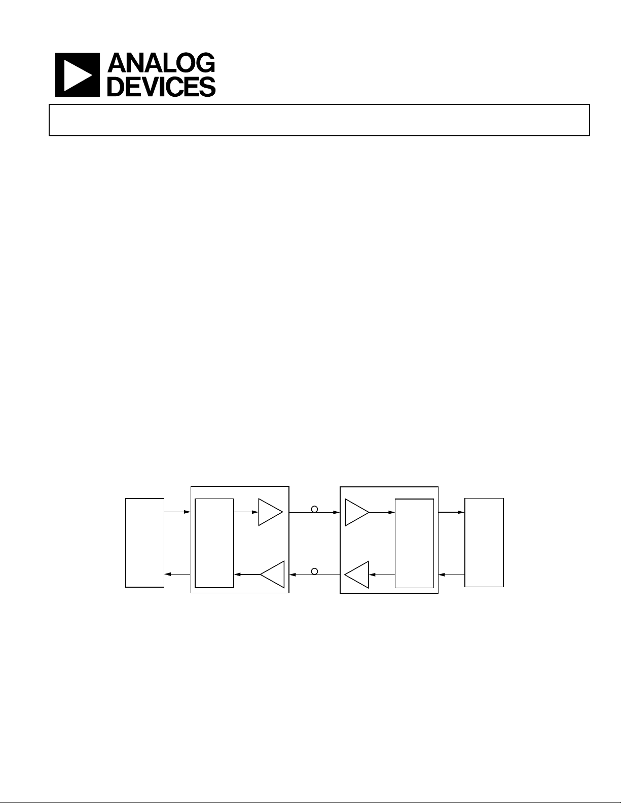
XFP MODULE
TXDATA
12” FR4
OTX
ADN2928
PRODUCT OVERVIEW
The ADN2928 provides the transmit and receive functions of
quantization, loss of signal detect, and clock and data recovery
at rates from 9.953 Gbps to 11.1 Gbps. The part is designed with
the flexibility to allow it to be used in either Telecoms or
Datacoms XFP module applications. The key advantages of this
circuit’s delay and phase-locked loop architecture are that it
provides a low jitter transfer bandwidth of 1 MHz, while also
exceeding the jitter tolerance requirements of XFP, SONET,
Gigabit Ethernet and Fibre Channel. The architecture also
provides fundamentally 0 dB of Jitter peaking.
XFP MODULE
ORX
12” FR4
RXDATA
SERDES/
ASIC
RXDATA
Rev. PrB
Information furnished by Analog Devices is believed to be accurate and reliable.
However, no responsibility is assumed by Analog Devices for its use, nor for any
infringements of patents or other rights of third parties that may result from its use.
Specifications subject to change without notice. No license is granted by implication
or otherwise under any patent or patent rights of Analog Devices. Trademarks and
registered trademarks are the property of their respective owners.
12” FR4
ADN2928
ORX
Figure 1. Typical XFP Application
12” FR4
SERDES/
ASIC
TXDATA
05264-001
ADN2928
OTX
One Technology Way, P.O. Box 9106, Norwood, MA 02062-9106, U.S.A.
Tel: 781.329.4700
Fax: 781.461.3113
www.analog.com
© 2005 Analog Devices, Inc. All rights reserved.

ADN2928 Preliminary Technical Data
TABLE OF CONTENTS
Functional Block Diagram .............................................................. 3
Receive Path Specifications ............................................................. 4
Transmit Path Specifications........................................................... 5
Common Specifications................................................................... 6
Absolute Maximum Ratings............................................................ 7
Pin Configuration and Function Descriptions............................. 8
General Description ......................................................................... 9
2
I
C Interface .................................................................................. 9
Receive Path .................................................................................. 9
Transmit Path................................................................................ 9
System Functions.......................................................................... 9
Applications Information .............................................................. 10
PCB Design Guidelines ............................................................. 10
Outline Dimensions....................................................................... 11
Ordering Guide........................................................................... 11
REVISION HISTORY
3/05—Revision PrB: Preliminary Version
Rev. PrB | Page 2 of 12
Preliminary Technical Data ADN2928
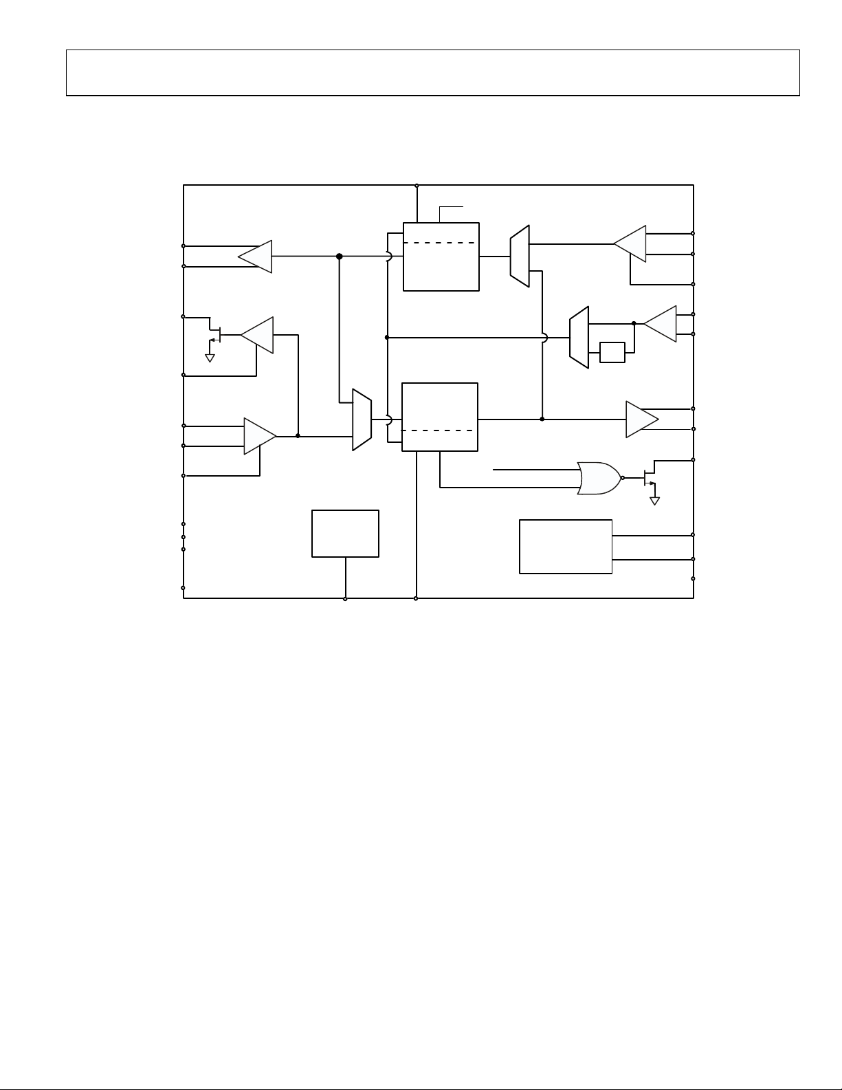
FUNCTIONAL BLOCK DIAGRAM
CFT
TxOUTP
TxOUTN
RxLOS
RxTHR
RxINP
RxINN
COSR
VDDT_1.8
VDDR_1.8
VDD_3.3
GN D
LimitingAmp
1.0V
regulator
CVDD_1.0
FL L
TxCDR
RxC DR
FL L
CFR
RxLOL
TxLOL
TxLOL
I2C
REGISTERS
Equalizer
4
4
TxINP
TxINN
COST
REFCKP
REFCKN
RxOUTP
RxOUT N
CDR_NR
SCK
SDA
PDN
Figure 2. ADN2928 Functional Block Diagram
Rev. PrB | Page 3 of 12

ADN2928 Preliminary Technical Data
RECEIVE PATH SPECIFICATIONS
Table 1.
PARAMETER Conditions Min Typ Max Unit
QUANTIZER DC CHARACTERISTICS ac coupled, PIN-NIN
Peak-to-Peak Differential Input
Input Sensitivity, VSENSE 10 mV
Input Offset Voltage 1 mV
Input Current µA
Input RMS Noise 365 µV
QUANTIZER AC CHARACTERISTICS Differential
−3 dB Bandwidth
Input Data Rate 9.953 11.1 Gbps
Small Signal Gain 45 dB
S11
Random Jitter 0.3 ps rms
Input Resistance 100 Ω
Input Capacitance TBD pF
Power Supply Rejection 100 mV p-p @ 100 MHz on VDD 60 dB
LEVEL DETECT
LOS Signal Level 5 mV
Hysteresis 3 dB
PHASE-LOCKED LOOP CHARACTERISTICS
For All Input Data Rates
Jitter Transfer BW - Telecoms 1.2 3 MHz
Jitter Transfer BW - Datacoms 1.2 3 MHz
Jitter Tolerance - Telecoms
Sinusoidal Jitter Tolerance Meets SONET mask.
Jitter Tolerance - Datacoms
Sinusoidal Jitter Tolerance Meets 802.3ae mask
Jitter Generation rms 0.7 ps rms
Jitter Peaking Measured 50 kHz – 80 MHz
< 120 kHz 0 dB
> 120 kHz 0 dB
CML OUTPUTS - RxOUTP/N
Single-Ended Output Swing Vse 200 425 mV
Differential Output Swing Vdiff 400 850 mV
Output High Voltage Voh TBD
Output Low Voltage Vol TBD
Rise Time 20% – 80% 24 ps
Fall Time 80% – 20% 24 ps
PIN-NIN, BER < 10
@ 10 GHz 10 GHz
−12
1.8 V
−12
dB
Rev. PrB | Page 4 of 12

Preliminary Technical Data ADN2928
TRANSMIT PATH SPECIFICATIONS
Table 2.
PARAMETER Conditions Min Typ Max Unit
QUANTIZER DC CHARACTERISTICS ac coupled, PIN – NIN
Peak-to-Peak Differential Input
Input Sensitivity, VSENSE 40 mV
Input Offset Voltage 1 mV
Input Current µA
Input RMS Noise µV
QUANTIZER AC CHARACTERISTICS Differential
−3dB Bandwidth
Input Data Rate 9.953 11.1 Gbps
Small Signal Gain 32 dB
S11
Random Jitter 0.3 ps rms
Input Resistance 100 Ω
Input Capacitance TBD pF
Power-Supply Rejection 100 mV p-p @ 100 MHz on VDD 60 dB
PHASE-LOCKED LOOP CHARACTERISTICS
For All Input Data Rates
Jitter Transfer BW 1.2 3 MHz
Jitter Tolerance - Telecoms
Sinusoidal Jitter Tolerance Meets SONET mask.
Jitter Tolerance - Datacoms
Sinusoidal Jitter Tolerance Meets 802.3ae mask
Jitter Generation rms 0.7 pS rms
Jitter Peaking Measured 50 kHz – 80 MHz
< 120 kHz 0 dB
> 120 kHz 0 dB
CML OUTPUTS - TxOUTP/N
Single-Ended Output Swing Vse 300 500 mV
Differential Output Swing Vdiff 700 1000 mV
Output High Voltage Voh TBD
Output Low Voltage Vol TBD
Rise Time 20% – 80% 24 ps
Fall Time 80% – 20% 24 ps
PIN – NIN, BER < 10
@ 10 GHz 10 GHz
−12
1.8 V
−12
dB
Rev. PrB | Page 5 of 12

ADN2928 Preliminary Technical Data
COMMON SPECIFICATIONS
Table 3.
PARAMETER Conditions Min Typ Max Unit
POWER-SUPPLY VOLTAGE, VDD_3.3 3 3.3 3.6 V
POWER-SUPPLY VOLTAGE, VDDx_1.8 1.6 1.8 2.0 V
POWER SUPPLY CURRENT, VDD_3.3 mA
POWER SUPPLY CURRENT, VDDx_1.8 mA
POWER 760 mW
RECEIVE REFERENCE CLOCK INPUTS
Clock Frequency CTRL[0]=0 155 MHz
Clock Frequency CTRL[0]=1 622 MHz
Input Voltage Range V
Rev. PrB | Page 6 of 12

Preliminary Technical Data ADN2928
ABSOLUTE MAXIMUM RATINGS
Table 4.
Parameter Rating
Supply Voltage 5 V
Input Voltage (Pin x or Pin x to Vcc) TBD
Maximum Junction Temperature 165°C
Storage Temperature Range
Lead Temperature (Soldering 10 sec) 300°C
ESD Rating (Human Body Model) TBD V
ESD (electrostatic discharge) sensitive device. Electrostatic charges as high as 4000 V readily accumulate on
the human body and test equipment and can discharge without detection. Although this product features
proprietary ESD protection circuitry, permanent damage may occur on devices subjected to high energy
electrostatic discharges. Therefore, proper ESD precautions are recommended to avoid performance
degradation or loss of functionality.
−65°C to +150°C
Stresses above those listed under Absolute Maximum Ratings
may cause permanent damage to the device. This is a stress
rating only; functional operation of the device at these or any
other conditions above those indicated in the operational
section of this specification is not implied. Exposure to absolute
maximum rating conditions for extended periods may affect
device reliability.
Rev. PrB | Page 7 of 12

ADN2928 Preliminary Technical Data
PIN CONFIGURATION AND FUNCTION DESCRIPTIONS
1
23
4567
A
B
C
D
E
F
G
Figure 3. Pin Configuration
Table 5. Pin Function Descriptions
Pin No. Mnemonic Type1 Description
A1, A4, B5, B6, D3 to D6, E3,
F2, F6, G4, G7
A7, C6, D7, E5, E6, F7 VDDT_1.8 P 1.8 V transmitter power supply
B1, C2, C3, D1, E4, G1 VDDR_1.8 P 1.8 V receiver power supply
C1, E7 VDD_3.3 P 3.3 V power supply
A2 RxINN AI Negative Differential Rx Data Input
A3 RxINP AI Positive Differential Rx Data Input
A5 TxOUTP AO Positive Differential Tx Data Output; CML
A6 TxOUTN AO Negative Differential Tx Data Output; CML
B2 RxTHR AI Receiver LOS Threshold Setting Resistor
B3 COSR AO Receiver Offset Compensation Loop Capacitor
B4 CVDD_1.0 P 100 nF Decoupling Capacitor for Internal 1 V digital supply
B7 NC No Connect
C4 REFCLKN AI Negative Differential Reference Clock Input
C5 REFCLKP AI Positive Differential Reference Clock Input
C7 CFT AO Transmitter FLL Loop Filter Capacitor
D2 RxLOS DO Receiver Loss of Signal Alarm Output. Active High
E1 CFR AO Receiver FLL Loop Filter Capacitor
E2 PDN DI Chip Power Down Input
F1 CDR_NR DO CDR Not Ready Alarm. Active High.
F3 SDA DI/O I
F4 SCK DI I
F5 COST AO Transmitter Offset Compensation Loop Capacitor
G2 RxOUTN AO Negative Differential Rx Data Output; CML
G3 RxOUTP AO Positive Differential Rx Data Output; CML
G5 TxINN AI Negative Differential Tx Data Input
G6 TxINP AI Postive Differential Tx Data Input
1
Type: P = power, AI = analog input, AO = analog output, DI = digital input, DO = digital output.
GND P Ground
2
C Serial Data Input.
2
C Serial Clock Input
Rev. PrB | Page 8 of 12

Preliminary Technical Data ADN2928
GENERAL DESCRIPTION
The ADN2928 provides the transmit and receive functions of
quantization, loss of signal detect, and clock and data recovery
at rates from 9.953 Gbps to 11.1 Gbps. The part is designed
with the flexibility to allow it to be used in either Telecoms or
Datacoms XFP module applications.
I2C INTERFACE
The I2C interface is used to control the following functions:
data invert and squelch, lineside loop-back, XFI system loopback, REFCLK divide ratio, status readback, optional equalizer
control, and software reset.
RECEIVE PATH
Limiting Amplifier
A limiting amplifier on the data inputs RxINP/N, of the device
has differential inputs which are internally terminate with
50 Ω to an on-chip reference voltage. The limiting amplifier
quantizes the data, with a sensitivity of better than 10 mV.
Loss of Signal Detector
The receiver front end signal-level detector indicates when the
input level has dropped below a user-adjustable level, by asserting Pin LOS to logic high. The trip point can be varied by an
external resistor. The signal-level detector circuitry has a comparator with a minimum hysteresis of 3 dB to prevent chatter.
Clock and Data Recovery PLL
The receive path clock and data recovery (CDR) block recovers
the clock from the serial data input and provides proper timing
for the data outputs. This block contains a synthesizerfrequency tracking loop, and a data-phase tracking loop. A
synthesizer tracking loop locks the divided-down clock derived
from the VCO frequency to a local reference clock running at
1/64 or 1/16 the input data rate. Once it is determined that the
VCO frequency is locked to the reference clock and that valid
serial data is present at the input, then the synthesizer loop is
switched off, and the data-phase tracking loop is turned on.
The data-phase tracking loop is designed in a manner such
that, once locked, the sampling edge of the VCO clock is automatically aligned with the center of the data input. A key feature
of the delay and phase-locked loop (DPLL) architecture is that,
unlike an ordinary PLL, it provides for 0 dB jitter peaking.
CML Outputs
The data signal that is retimed by the CDR clock is driven offchip by 50 Ω terminated current mode logic line drivers. The
data polarity can be optionally inverted through the I
face, and can be squelched. Output amplitudes can be adjusted.
Lock Detector
The lock detector monitors the frequency difference between
the VCO and the reference clock and asserts a lock signal
(RxLOCK) when the VCO is within 500 ppm of the center
frequency. This enables the phase loop which maintains phase
lock, unless the frequency error exceeds 1000 ppm.
2
C inter-
TRANSMIT PATH
Equalizer
An equalizer on the data inputs TxINP/N, of the ADN2928
has differential inputs which are internally terminated with
50 ohms to an on chip reference voltage. The equalizer compensates for the ISI induced signal distortion resulting from up to
12 inches of FR4, plus one connector. This enables the CDR to
retime the data from signals transmitted over standard XFI
interfaces. The equalizer characteristics have been optimized
such that no user programming is required to achieve low
retiming error rates for all data rates and XFI compliant
channels. However for other applications the equalizer boost
characteristics can be programmed through the I2C interface.
Clock and Data Recovery PLL
The transmit path clock and data recovery (CDR) block
recovers the clock from the serial data input and provides
proper timing for the data outputs. This block contains a
synthesizer frequency tracking loop, and a data phase tracking
loop. A synthesizer tracking loop locks the divided down clock
derived from the VCO frequency to a local reference clock
running at 1/ 64 or 1/16 the input data rate. Once it is
determined that the VCO frequency is locked to the reference
clock and valid serial data is present at the input, then the
synthesizer loop is switched off, and the data phase tracking
loop is turned on. The data phase tracking loop is designed in a
manner such that, once locked, the sampling edge of the VCO
clock is automatically aligned with the center of the data input.
A key feature of the Delay and Phase Locked Loop (DPLL)
architecture used is that unlike an ordinary PLL, it provides for
0 dB jitter peaking.
CML Outputs
The data signal that is retimed by the CDR clock is driven offchip by 50 Ω terminated current-mode logic line drivers. The
data polarity can be optionally inverted through the I
face, and can be squelched. Output amplitudes can be adjusted.
2
C inter-
Lock Detector
The lock detector monitors the frequency difference between
the VCO and the reference clock and asserts a lock signal
(TxLOCK) when the VCO is within 500 ppm of the center
frequency. This enables the phase loop which maintains phase
lock, unless the frequency error exceeds 1000 ppm.
SYSTEM FUNCTIONS
XFI System Loopback
In this mode data received on the TxINP/N pins is retimed and
output on the RxOUTP,N pins. The TxINP/N data is not
present on the TxOUTP/N pins.
Lineside Loopback
In this mode data received on the RxINP/N pins is retimed and
output on the TxOUTP/N pins. The received data is not present
on the RxOUTP/N pins.
Rev. PrB | Page 9 of 12

ADN2928 Preliminary Technical Data
APPLICATIONS INFORMATION
PCB DESIGN GUIDELINES
Proper RF PCB design techniques must be used for optimal
performance. A typical ADN2928 applications circuit is shown
in Figure 4.
Power Supply Connections and Ground Planes
Using one low impedance ground plane is recommended.
Solder the GND pins directly to the ground plane to reduce
series inductance. If the ground plane is an internal plane and
connections to the ground plane are made through vias, multiple vias can be used in parallel to reduce the series inductance.
Use of a 22 µF electrolytic capacitor between each supply
and GND is recommended at the location where the supply
enters the PCB. Use 0.1 µF and 1 nF ceramic chip capacitors to
decouple the IC power supplies between VDD and VEE. These
caps should be placed as close as possible to the ADN2928
VDD pins.
If connections to the supply and ground are made through vias,
the use of multiple vias in parallel helps to reduce series
inductance.
Transmission Lines
Use of 50 Ω transmission lines is required for all high frequency
input and output signals to minimize reflections: RxINN/P,
RxOUTN/P, TxINN/P, TxOUTN/P, REFCLKN/P. It is also
necessary for the differential pairs to be matched in length to
avoid skew between the differential traces. As with any high
speed mixed-signal design, take care to keep all high speed
digital traces away from sensitive analog nodes.
PD_VCC
1.8V
AD N 2525 for LD
AD N 2530 for VCSEL
AD N 2849 for EAM
LDD
ADN 2821
TIA
1000p
RTH
100n
100n
100n
100n
VDDT_1.8
22uF
VDDR_1.8
22uF
VDDT_1.8
A5
A6
A3
A2
COSR
B3
RxTHR
B2
1
B
50 50
100n
2
C
3
C
1
4
D
E
CM L
PA
LOS
1n
1
G
1n and 100n
decoupling caps
placed right at DUT
1n
7
6
7
5
6
7
A
E
C
D
E
F
CFT
TxCDR
RxCDR
CFR
100n
100n 22u
1
C
REFCL K
CM L
7
E
1.0V
regulator
EQ
VDDR_1.8
4
B
50 50
VDD_3.3
CVDD_1.0
COST
RxLOS
VDD T _1.8
C7
G6
G5
F5
C5
C4
G3
G2
VDDR_1.8
68n
E1
D2
VDD_3.3
100n
100n
1000p
100n
100n
100n
100n
100n
68n
XFI
VDD_3.3
4.7k
(thispull-up
on host PCB)
I2C
Registers
G7G4F6F2E3D6D5D4D3B6B5A4A1
Figure 4. Typical ADN2928 Applications Circuit
Rev. PrB | Page 10 of 12
SCK
SDA
CDR_NR
PDN
1.2k
F4
F3
F1
E2
VDD_3.3
4.7k
1.2k
ADuC7020

Preliminary Technical Data ADN2928
A
R
OUTLINE DIMENSIONS
1 CORNE
INDEX AREA
63
BOTTOM
2
VIEW
DETAILA
*
0.50
0.45
0.40
SEATING
PLANE
1
A
B
C
D
E
F
G
1.31
1.21
1.10
COPLANARITY
0.12 MAX
1.50
SQ
1.70
1.56
1.35
6.00
BSC SQ
BALL A1
PAD CORNER
TOP VIEW
DETAIL A
745
4.80
BSC SQ
0.80
BSC
0.35
0.25
BALL DIAMETER
*
COMPLIANT TO JEDEC STANDARDS MO-205
WITH THE EXCEPTION OF BALL DIAMETER.
Figure 5. 49-Lead Chip Scale Package Ball Grid Array [CSP_BGA]
(BC-49-2)
Dimensions shown in millimeters
ORDERING GUIDE
Model Temperature Range Package Description Package Option
ADN2928 0° to 85°C
Rev. PrB | Page 11 of 12

ADN2928 Preliminary Technical Data
NOTES
Purchase of licensed I
Rights to use these components in an I
2
C components of Analog Devices or one of its sublicensed Associated Companies conveys a license for the purchaser under the Philips I2C Patent
2
C system, provided that the system conforms to the I2C Standard Specification as defined by Philips.
© 2005 Analog Devices, Inc. All rights reserved. Trademarks and
registered trademarks are the property of their respective owners.
PR05264–0–3/05(PrB)
Rev. PrB | Page 12 of 12
 Loading...