3.3 V 4.25 Gb/s
Preliminary Technical Data
FEATURES
SFP reference design available
Input sensitivity: 3 mV p-p
65 ps rise/fall times
BW Select to support Multi-Rate 1x/2x/4x FC modules
Optional LOS Output Inversion to support SFF
CML outputs: 700 mV p-p differential
Programmable LOS detector: 3 mV to 45 mV
Rx signal strength indicator (RSSI):
SFF-8472 compliant average power measurement
Single supply operation: 3.3 V
Low power dissipation: 160 mW
Available in space-saving 3 × 3 mm 16-lead LFCSP
Increased Temperature Range: -40
APPLICATIONS
SFP/SFF/GBIC optical transceivers
1x/2x/4x Multi-rate Fibre Channel receivers
LX4
WDM transponders
PRODUCT OVERVIEW
o
C to 95oC
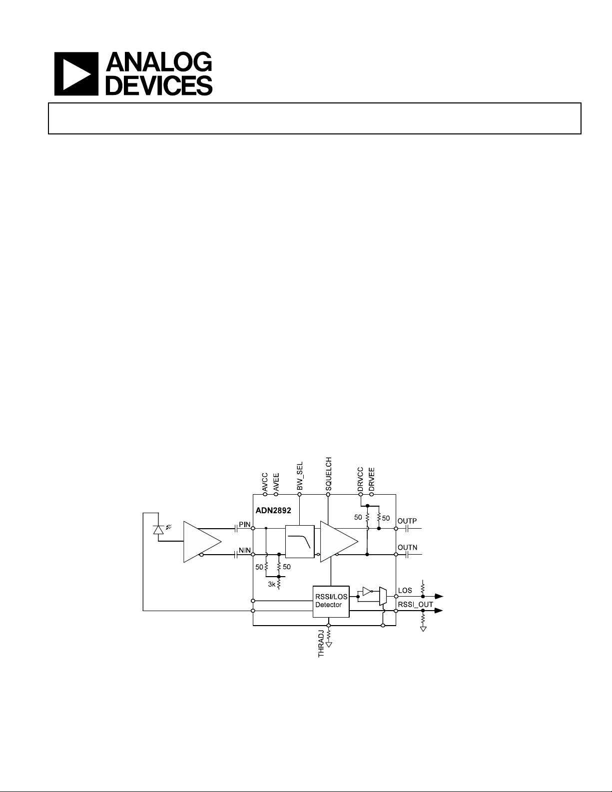
FUNCTIONAL BLOCK DIAGRAM
Limiting Amplifier
ADN2892
The ADN2892 is a high gain, limiting amplifier optimized for
use in Fibre Channel and GbE optical receivers. The ADN2892
accepts input levels of up to 2.0 V p-p differential and has 3 mV
p-p differential input sensitivity. The ADN2892 provides the
receiver functions of quantization and loss of signal (LOS)
detection.
The ADN2892 has an on-chip selectable filter to reduce the BW
of the limamp to 1.5GHz in order to filter out the relaxation
oscillation of legacy 1Gb/s Fiber Channel transmitters with CD
lasers. The reduced BW will also allow for more optical Rx
sensitivity margin at the lower data rates such as 1xFC and
1GbE in multi-rate modules.
The limiting amplifier also measures average received power
based on a direct measurement of the photodiode current with
better than 1 dB of accuracy over the entire input range of the
receiver. This eliminates the need for external average Rx power
detection circuitry in SFF-8472 compliant optical transceivers.
The ADN2892 limiting amplifier operates from a single 3.3 V
supply, has low power dissipation, and is available in a spacesaving 3 × 3 mm 16-lead lead frame chip scale package
(LFCSP).
ADN2882
V
PD_VCC
PD_CATHODE
REF
Rev. PrA.
Information furnished by Analog Devices is believed to be accurate and reliable.
However, no responsibility is assumed by Analog Devices for its use, nor for any
infringements of patents or other rights of third parties that may result from its use.
Specifications subject to change without notice. No license is granted by implication
or otherwise under any patent or patent rights of Analog Devices. Trademarks and
registered trademarks are the property of their respective owners.
Figure 1.
+V
10kΩ
ADuC7020
V
N
I
_
S
O
L
One Technology Way, P.O. Box 9106, Norwood, MA 02062-9106, U.S.A.
Tel: 781.329.4700 www.analog.com
Fax: 781.326.8703 © 2004 Analog Devices, Inc. All rights reserved.

ADN2892 Preliminary Technical Data
TABLE OF CONTENTS
Specifications..................................................................................... 3
Loss of Signal (LOS) Detector .....................................................8
Absolute Maximum Ratings............................................................ 5
Thermal Resistance ...................................................................... 5
ESD Caution.................................................................................. 5
Pin Configuration and Function Descriptions............................. 6
Typical Performance Characteristics ............................................. 7
Theory of Operation ........................................................................ 8
LIMAMP ....................................................................................... 8
REVISION HISTORY
Revision A: Initial Version
Received Signal Strength Indicator (RSSI) ................................8
Squelch Mode ................................................................................8
Applications Information.................................................................9
PCB Design Guidelines ................................................................9
Outline Dimensions....................................................................... 11
Ordering Guide .......................................................................... 11
Rev. PrA| Page 2 of 12

Preliminary Technical Data ADN2892
SPECIFICATIONS
VCC = V
Table 1.
Parameter Min Typ Max Unit Test Conditions/Comments
QUANTIZER DC CHARACTERISTICS
Input Voltage Range 1.8 2.8 V p-p @ PIN or NIN, dc-coupled
Input Common Mode 2.1 2.7 V DC-coupled
Peak-to-Peak Differential Input Range 2.0 V p-p PIN − NIN, ac-coupled
Input Sensitivity 3 mV p-p
Input Offet Voltage 100 µV
Input RMS Noise 205 µV rms
Input Resistance 50 Ω Single-ended
Input Capacitance 0.65 pF
QUANTIZER AC CHARACTERISTICS
Input Data Rate 1.0
Small Signal Gain 51 dB Differential
S11 -15 dB Differential, f < 4.25 GHz
S22 -15 dB Differential, f < 4.25 GHz
Random Jitter 5 ps rms Input > 10 mV p-p, 4.25Gb/s, PRBS 27 − 1
Deterministic Jitter 10 ps p-p Input > 10 mV p-p, 4.25 Gb/s, PRBS 27 − 1
Low Frequency Cutoff 30 kHz
Power Supply Noise Rejection 45 dB f < 10 MHz
LOSS OF SIGNAL DETECTOR (LOS)
LOS Assert Level TBD 3.0 TBD mV p-p R
TBD 45.0 TBD mV p-p R
LOS Hysteresis 3 TBD dB 4.25Gb/s, PRBS 27 − 1, R
TBD 3 dB 4.25Gb/s, PRBS 27 − 1, R
LOS Assert Time 600 ns DC-coupled
LOS De-Assert Time 100 ns DC-coupled
RSSI
Input Current Range 5 1000 µA
RSSI Output Accuracy 15 %
10 % IIN > 20 µA
Gain 1.0 mA/mA I
Offset 50 nA
Compliance Voltage VCC − 0.9 VCC − 0.3 V @ PD_CATHODE
POWER SUPPLIES
VCC 3.0 3.3 3.6 V
ICC 50 mA
OPERATING TEMPERATURE RANGE −40 +25 +95 °C T
CML OUTPUT CHARACTERISTICS
Output Impedance 50 Ω Single-ended
Output Voltage Swing 600 700 800 V p-p Differential
Output Rise and Fall Time 65 ps 20% to 80%
LOGIC INPUTS
VIH, Input High Voltage 2.0 V
VIL, Input Low Voltage 0.8 V
Input Current −100 nA I
100 nA I
MIN
to V
, VEE = 0 V, TA = T
MAX
MIN
to T
, BW_SEL = 1, unless otherwise noted.
MAX
4.25
1.0
2.125
Gb/s
Gb/s
PIN − NIN, BER ≤ 1 × 10
BW_SEL = 1
BW_SEL = 0
= 100 kΩ
THRADJ
= 0 Ω
THRADJ
I
≤ 20 µA
IN
RSSI/IPD
to T
MAX
MIN
, VIN = 2.4 V
INH
, VIN = 0.4 V
INL
−10
THRADJ
THRADJ
= 0 Ω
= 100 kΩ
Rev. PrA | Page 3 of 12

ADN2892 Preliminary Technical Data
Parameter Min Typ Max Unit Test Conditions/Comments
LOGIC OUTPUTS (LOS)
VOH, Output High Voltage 2.4 V
VOL, Output Low Voltage 0.4 V
Open drain output, 4.7 kΩ − 10 kΩ
pull-up resistor to V
Open drain output, 4.7 kΩ − 10 kΩ
pull-up resistor to VCC
CC
Rev. PrA| Page 4 of 12
 Loading...