

查询ADN2892供应商
3.3 V, 4.25 Gbps,
FEATURES
Input sensitivity: 3.5 mV p-p
70 ps rise/fall times
CML outputs: 750 mV p-p differential
Bandwidth selectable for multirate 1×/2×/4× FC modules
Optional LOS output inversion
Programmable LOS detector: 3.5 mV to 35 mV
Rx signal strength indicator (RSSI)
SFF-8472-compliant average power measurement
Single-supply operation: 3.3 V
Low power dissipation: 160 mW
Available in space-saving, 3 mm × 3 mm, 16-lead LFCSP
Extended temperature range: −40°C to +95°C
SFP reference design available
APPLICATIONS
1×, 2×, and 4× FC transceivers
SFP/SFF/GBIC optical transceivers
GbE transceivers
Backplane receivers
Limiting Amplifier
ADN2892
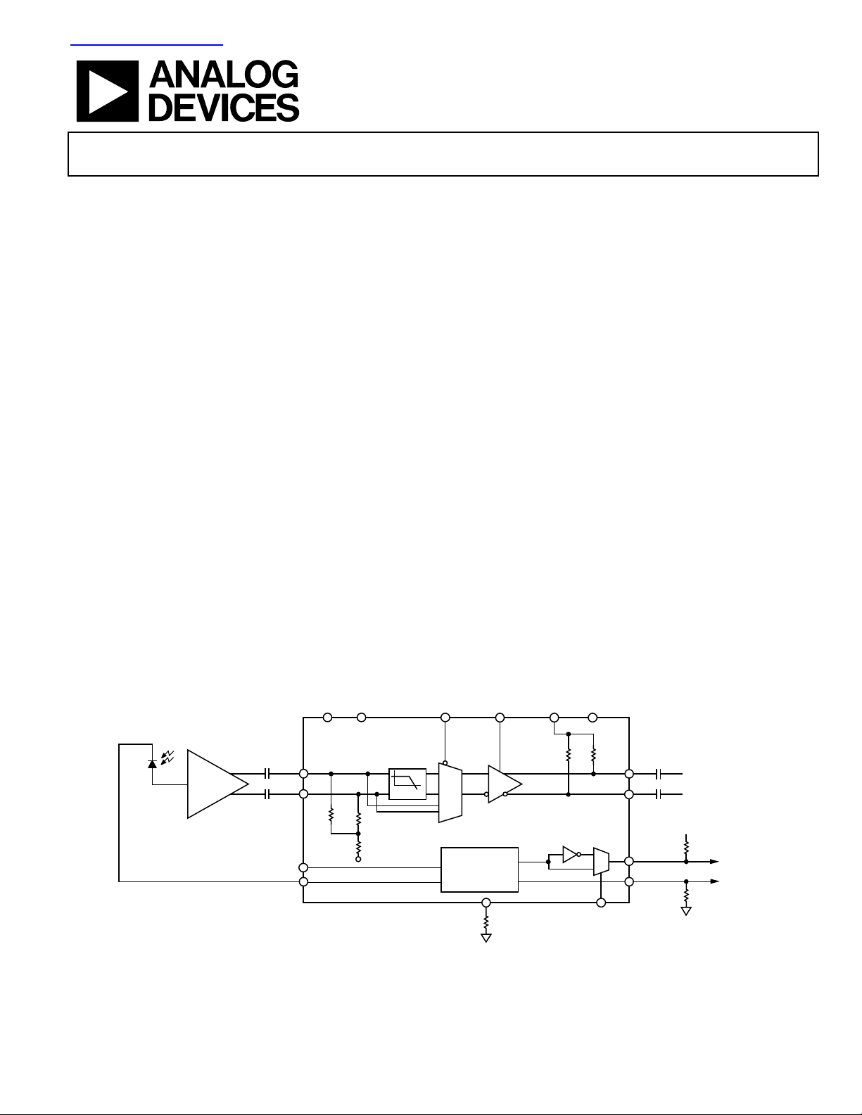
GENERAL DESCRIPTION
The ADN2892 is a 4.25 Gbps limiting amplifier with integrated
loss of signal (LOS) detection circuitry and a received signal
strength indicator (RSSI). This part is optimized for Fibre
Channel (FC) and Gigabit Ethernet (GbE) optoelectronic
conversion applications. The ADN2892 has a differential input
sensitivity of 3.5 mV p-p and accepts up to a 2.0 V p-p
differential input overload voltage. The ADN2892 has current
mode logic (CML) outputs with controlled rise and fall times.
The ADN2892 has a selectable low-pass filter with a −3 dB
cutoff frequency of 1.5 GHz. By setting BW_SEL to Logic 0, the
filter can limit the relaxation oscillation of a low cost CD laser
used in a legacy 1 Gbps FC transmitter. The limited BW also
reduces the rms noise and in turn improves the receiver optical
sensitivity for a lower data rate application, such as 1× FC and
GbE.
By monitoring the bias current through a photodiode, the onchip RSSI detector measures the average power received with
2% typical linearity over the entire valid input range of the
photodiode. The on-chip RSSI detector facilitates SFF-8472compliant optical transceivers by eliminating the need for
external RSSI detector circuitry.
FUNCTIONAL BLOCK DIAGRAM
AVCC
AVEE
ADN2892
PIN
ADN2882
Rev. 0.
Information furnished by Analog Devices is believed to be accurate and reliable.
However, no responsibility is assumed by Analog Devices for its use, nor for any
infringements of patents or other rights of third parties that may result from its use.
Specifications subject to change without notice. No license is granted by implication
or otherwise under any patent or patent rights of Analog Devices. Trademarks and
registered trademarks are the property of their respective owners.
NIN
PD_VCC
PD_CATHODE
LPF
50Ω
50Ω
3.5kΩ
V
REF
Figure 1. RSSI Function Capable—Applications Setup Block Diagram
Additional features include a programmable loss-of-signal
(LOS) detector and output squelch. The ADN2892 is available
in a 3 mm × 3 mm, 16-lead LFCSP.
BW_SEL SQUELCH
RSSI/LOS
DETECTOR
THRADJ
One Technology Way, P.O. Box 9106, Norwood, MA 02062-9106, U.S.A.
Tel: 781.329.4700
Fax: 781.461.3113 ©2005 Analog Devices, Inc. All rights reserved.
DRVEE
DRVCC
50Ω 50Ω
LOS_INV
www.analog.com
OUTP
OUTN
LOS
RSSI_OUT
V+
10kΩ
ADuC7020
04986-001

ADN2892
TABLE OF CONTENTS
Specifications..................................................................................... 3
Squelch Mode ............................................................................. 10
Absolute Maximum Ratings............................................................ 5
Thermal Resistance ...................................................................... 5
ESD Caution.................................................................................. 5
Pin Configuration and Function Descriptions............................. 6
Typical Performance Characteristics ............................................. 7
Theory of Operation ...................................................................... 10
Limiting Amplifier ..................................................................... 10
Loss-of-Signal (LOS) Detector ................................................. 10
Received Signal Strength Indicator (RSSI).............................. 10
REVISION HISTORY
4/05—Revision 0: Initial Version
BW_SEL (Bandwidth Selection) Mode................................... 10
LOS_INV (Lose of Signal_Invert) Mode................................ 10
Applications..................................................................................... 11
PCB Design Guidelines ............................................................. 11
Pad Coating and Pb-Free Soldering ........................................ 12
Outline Dimensions ....................................................................... 13
Ordering Guide .......................................................................... 13
Rev. 0 | Page 2 of 16
ADN2892
SPECIFICATIONS
Test Conditions: VCC = 2.9 V to 3.6 V, VEE = 0 V, TA = −40°C to +95°C, unless otherwise noted.
Table 1.
Parameter Min Typ Max Unit Test Conditions/Comments
QUANTIZER DC CHARACTERISTICS
Input Voltage Range VCC − 1.2 VCC − 0.2 V At PIN or NIN, dc-coupled
Input Common Mode 2.1 2.7 V DC-coupled
Peak-to-Peak Differential Input Range 2.0 V p-p PIN − NIN, ac-coupled
Input Sensitivity 6.6 3.5 mV p-p PIN − NIN, BER ≤ 1 × 10
Input Offset Voltage 100 µV
Input RMS Noise 235 µV rms
Input Resistance 50 Ω Single-ended
Input Capacitance 0.65 pF
QUANTIZER AC CHARACTERISTICS
Input Data Rate 1.0 4.25 Gbps
Small Signal Gain 51 dB Differential
S11 −10 dB Differential, f < 4.25 GHz
S22 −10 dB Differential, f < 4.25 GHz
Random Jitter 3.0 3.9 ps rms Input ≥ 10 mV p-p, 4× FC, K28.7 pattern
Deterministic Jitter 10 21.0 ps p-p Input ≥ 10 mV p-p, 4× FC, K28.5 pattern
Low Frequency Cutoff 30 kHz
Power Supply Rejection 45 dB 100 kHz < f < 10 MHz
LOSS OF SIGNAL DETECTOR (LOS)
LOS Assert Level 2.9 3.5 4.8 mV p-p R
22.4 35 55.0 mV p-p R
THRADJ
THRADJ
= 100 kΩ
= 1 kΩ
Electrical Hysteresis 2.5 5.0 dB 1.0 Gbps, PRBS 223 − 1
2.8 5.0 dB 4× FC, PRBS 223 − 1
LOS Assert Time 950 ns DC-coupled
LOS Deassert Time 62 ns DC-coupled
RSSI
Input Current Range 5 1000 µA
RSSI Output Linearity 2 % 5 µA ≤ IIN ≤ 1000 µA
Gain 1.0 mA/mA I
RSSI/IPD_CATHODE
Offset 145 nA
Compliance Voltage (At PD_CATHODE) VCC − 0.4 V I
V
− 0.9 V I
CC
PD_CATHODE
PD_CATHODE
= 5 µA
= 1000 µA
BW_SEL (BANDWIDTH SELECTION)
Channel Bandwidth 1.5 GHz
−3 dB cutoff frequency of the on-chip,
two-pole, low-pass filter, when BW_SEL = 0
POWER SUPPLIES
V
CC
I
CC
OPERATING TEMPERATURE RANGE −40 +25 +95 °C T
2.9 3.3 3.6 V
48 54 mA
to T
MIN
MAX
CML OUTPUT CHARACTERISTICS
Output Impedance 50 Ω Single-ended
Output Voltage Swing 600 750 940 V p-p Differential
Output Rise and Fall Time 70 103 ps 20% to 80%
−10
Rev. 0 | Page 3 of 16
ADN2892
Parameter Min Typ Max Unit Test Conditions/Comments
LOGIC INPUTS (SQUELCH, LOS_INV, AND
BW_SEL)
VIH, Input High Voltage 2.0 V
VIL, Input Low Voltage 0.8 V
Input Current (SQUELCH, LOS_INV) 39 µA
Input Current (BW_SEL) −38 µA
LOGIC OUTPUTS (LOS)
VOH, Output High Voltage 2.4 V
VOL, Output Low Voltage 0.4 V
, VIN = 2.4 V, 100 kΩ pull-down,
I
INH
on-chip resistor
, VIN = 0.0 V, 100 kΩ pull-up,
I
INL
on-chip resistor
Open drain output, 4.7 kΩ − 10 kΩ
pull-up resistor to VCC
Open drain output, 4.7 kΩ − 10 kΩ
pull-up resistor to VCC
Rev. 0 | Page 4 of 16
ADN2892
ABSOLUTE MAXIMUM RATINGS
Table 2.
Parameter Rating
Power Supply Voltage 4.2 V
Minimum Voltage
(All Inputs and Outputs)
Maximum Voltage
(All Inputs and Outputs)
Storage Temperature −65°C to +150°C
Operating Temperature Range −40°C to +95°C
Production Soldering Temperature J-STD-20
Junction Temperature 125°C
VEE − 0.4 V
VCC + 0.4 V
Stresses above those listed under Absolute Maximum Ratings
may cause permanent damage to the device. This is a stress
rating only and functional operation of the device at these or
any other conditions above those indicated in the operational
section of this specification is not implied. Exposure to absolute
maximum rating conditions for extended periods may affect
device reliability.
THERMAL RESISTANCE
θJA is specified for 4-layer PCB with exposed paddle soldered
to GND.
Table 3.
Package Type θ
3 mm × 3 mm, 16-lead LFCSP 28 °C/W
JA
Unit
ESD CAUTION
ESD (electrostatic discharge) sensitive device. Electrostatic charges as high as 4000 V readily accumulate on
the human body and test equipment and can discharge without detection. Although this product features
proprietary ESD protection circuitry, permanent damage may occur on devices subjected to high energy
electrostatic discharges. Therefore, proper ESD precautions are recommended to avoid performance
degradation or loss of functionality.
Rev. 0 | Page 5 of 16
ADN2892
PIN CONFIGURATION AND FUNCTION DESCRIPTIONS
PD_CATHODE
PD_VCC15RSSI_OUT
14
7
BW_SEL
SQUELCH
13
12
11
10
9
8
LOS
LOS_INV
DRVCC
OUTP
OUTN
DRVEE
04986-002
PIN
NIN
16
1
2
ADN2892
TOP VIEW
3
(Not to Scale)
4
5
6
THRADJ
AVCC
AVEE
Figure 2. Pin Configuration
Note that there is an exposed pad on the bottom of the package that must be connected to the GND plane with filled vias.
Table 4. Pin Function Descriptions
Pin No. Mnemonic I/O Type1Description
1 AVCC P Analog Power Supply.
2 PIN AI Differential Data Input, Positive Port, 50 Ω On-Chip Termination.
3 NIN AI Differential Data Input, Negative Port, 50 Ω On-Chip Termination.
4 AVEE P Analog Ground.
5 THRADJ AO LOS Threshold Adjust Resistor.
6 BW_SEL DI With one 100 kΩ on-chip, pull-up resistor, BW_SEL = 0 for 1×/2× FC, BW_SEL = 1 for 4× FC.
7 LOS_INV DI
With one 100 kΩ on-chip, pull-down resistor, LOS_INV = 1 inverts the LOS output
to be active low for SFF.
8 LOS DO LOS Detector Output, Open Collector.
9 DRVEE P Output Buffer Ground.
10 OUTN DO Differential Data Output, CML, Negative Port, 50 Ω, On-Chip Termination.
11 OUTP DO Differential Data Output, CML, Positive Port, 50 Ω, On-Chip Termination.
12 DRVCC P Output Buffer Power Supply.
13 SQUELCH DI Disable Outputs, 100 kΩ On-Chip, Pull-Down Resistor.
14 RSSI_OUT AO Average Current Output.
15 PD_VCC P Power Input for RSSI Measurement.
16 PD_CATHODE AO Photodiode Bias Voltage.
Exposed Pad Pad P Connect to Ground.
1
P = power; DI = digital input; DO = digital output; AI = analog input; and AO = analog output.
Rev. 0 | Page 6 of 16

ADN2892
TYPICAL PERFORMANCE CHARACTERISTICS
0.06
+95°C
0.05
0.04
+25°C
150mV/DIV
50ps/DIV
Figure 3. Eye of ADN2892 @ 25°C, 4.25 Gbps, and 10 mV Input
150mV/DIV
50ps/DIV
Figure 4. Eye of ADN2892 @ 95°C, 4.25 Gbps, and 10 mV Input
04986-012
04986-023
0.03
0.02
TRIP AND RELEASE (V)
0.01
0
1k 100k
8
7
6
5
4
3
2
ELECTRICAL HYSTERESIS (dB)
1
0
1k 100k
16
–40°C
–40°C
+25°C
+95°C
ASSERTION
10k
RTH (Ω)
Figure 6. LOS Trip and Release vs. R
1GBPS
4.25GBPS
10k
RTH (Ω)
Figure 7. LOS Electrical Hysteresis vs. R
DEASSERTION
at 4.25 Gbps
TH
at 25°C
TH
04986-026
04986-027
150mV/DIV
200ps/DIV
Figure 5. Eye of ADN2892 at 25°C, 1.063 Gbps, and 10 mV Input (BW_SEL = 0)
Rev. 0 | Page 7 of 16
04986-010
14
12
10
8
SAMPLES
6
4
2
0
5.8
6.0 6.2 6.4 6.6 6.8 7.0 7.2 7.4 7.6 7.8 8.0 8.2 8.4 8.6
ELECTRICAL HYSTERESIS (dB)
Figure 8. Sample Lot Distribution—Worst-Case Condition:
Conditions = 4.25 Gbps, 100 kΩ @ −40°C, 3.6 V
04986-024

ADN2892
4.0
1200
3.5
3.0
2.5
2.0
JITTER (ps)
1.5
1.0
0.5
0
1.0 4.5
1.5 2.0 2.5 3.0 3.5 4.0
RATE (Gbps)
Figure 9. Random Jitter vs. Data Rate
18
16
14
12
10
8
JITTER (ps)
6
04986-028
1000
800
600
400
RSSI OUTPUT CURRENT (µA)
200
0
0
200 400 600 800 1000
PD_CATHODE CURRENT (PHOTODIODE CURRENT) (µA)
Figure 12. RSSI Output vs. Average Photodiode Current
60
50
40
30
20
04986-017
4
2
0
1.0 4.5
1.5 2.0 2.5 3.0 3.5 4.0
RATE (Gbps)
Figure 10. Deterministic Jitter vs. Data Rate
70
60
50
40
30
20
10
POWER SUPPLY-NOISE REJECTION (dB)
0
100k
SUPPLY-NOISE FREQUENCY
1M
Figure 11. PSRR vs. Supply-Noise Frequency
10M
04986-029
04986-016
RSSI OUTPUT CURRENT (µA)
10
0
0
10 20 30 40 50
PD_CATHODE CURRENT (PHOTODIODE CURRENT) (µA)
Figure 13. RSSI Output vs. Average Photodiode Current (Zoomed)
–0.15
–0.20
–0.25
–0.30
–0.35
–0.40
–0.45
–0.50
–0.55
–0.60
–0.65
COMPLIANCE VOLTAGE REFERRED TO VCC (V)
–0.70
0 1000
100 200 300 400 500 600 700 800 900
INPUT CURRENT (µA)
Figure 14. PD_CATHODE Compliance Voltage vs.
Input Current RSSI (Refer to VCC)
04986-020
04986-018
Rev. 0 | Page 8 of 16

ADN2892
900
49.0
800
700
600
500
400
300
200
5µA REFERRED OFFSET (nA)
100
0
–40 100
–20 0 20 40 60 80
TEMPERATURE (°C)
Figure 15. RSSI Offset—Difference Between Measured RSSI Output and
PD_CATHODE (Input) Current of 5 µA
5.0
4.5
4.0
3.5
3.0
2.5
2.0
RSSI LINEARITY (%)
1.5
1.0
0.5
0
0 1000
200 400 600 800
+100°C
PD_CATHODE CURRENT (µA)
+30°C
–40°C
Figure 16. RSSI Linearity % vs. PD_CATHODE Current
04986-019
04986-021
48.5
48.0
47.5
(mA)
CC
I
47.0
46.5
46.0
–40–200 20406080
Figure 17. ADN2892 I
TEMPERATURE (°C)
Current vs. Temperature
CC
100
04986-025
Rev. 0 | Page 9 of 16

ADN2892
THEORY OF OPERATION
LIMITING AMPLIFIER
Input Buffer
The ADN2892 limiting amplifier provides differential
inputs (PIN/NIN), each with a single-ended, on-chip 50 Ω
termination. The amplifier can accept either dc-coupled or
ac-coupled signals; however, an ac-coupled signal is
recommended. Using a dc-coupled signal, the amplifier
needs a nominal VCC − 0.7 V common-mode voltage and
±0.5 V headroom. If the input common-mode voltage is 2.4 V,
the available headroom is reduced down to ±0.3 V.
RECEIVED SIGNAL STRENGTH INDICATOR (RSSI)
The ADN2892 has an on-chip, RSSI circuit. By monitoring the
current supplied to the photodiode, the RSSI circuit provides an
accurate, average power measurement. The output of the RSSI is
a current that is directly proportional to the average amount of
PIN photodiode current. Placing a resistor between the
RSSI_OUT pin and GND converts the current to a GND
referenced voltage. This function eliminates the need for
external RSSI circuitry for SFF-8472-compliant optical
receivers. For more information, see Figure 12 to Figure 16.
The ADN2892 limiting amplifier is a high gain device. It is
susceptible to dc offsets in the signal path. The pulse width
distortion presented in the NRZ data or a distortion generated
by the TIA may appear as dc offset or a corrupted signal to the
ADN2892 inputs. An internal offset correction loop can
compensate for certain levels of offset.
CML Output Buffer
The ADN2892 provides differential CML outputs, OUTP and
OUTN. Each output has an internal 50 Ω termination to VCC.
LOSS-OF-SIGNAL (LOS) DETECTOR
The on-chip LOS circuit drives LOS to logic high when the
input signal level falls below a user-programmable threshold.
The threshold level can be set anywhere from 3.5 mV pp to 35
mV pp typical by a resistor connected between the THRADJ
pin and VEE. See Figure 6 and Figure 7 for the LOS threshold
vs. THRADJ. The ADN2892 LOS circuit has an electrical
hysteresis greater than 2.5 dB to prevent chatter at the LOS
signal. The LOS output is an open-collector output that must be
pulled up externally with a 4.7 kΩ to 10 kΩ resistor.
Connect the PD_VCC, PD_CATHODE, and RSSI_OUT pins to
AVCC to disable the RSSI feature.
SQUELCH MODE
Driving the SQUELCH input to logic high disables the limiting
amplifier outputs. Using LOS output to drive the SQUELCH
input, the limiting amplifier outputs stop toggling anytime a
signal input level to the limiting amplifier drops below the
programmed LOS threshold.
The SQUELCH pin has a 100 kΩ, internal pull-down resistor.
BW_SEL (BANDWIDTH SELECTION) MODE
Driving the BW_SEL input signal to logic high, the amplifier
provides a 3.8 GHz bandwidth. Driving the BW_SEL input
signal to logic low, the amplifier accepts input signals through a
1.5 GHz, 2-pole, low-pass filter that improves receiving
sensitivity.
The low-pass filter reduces the possible relaxation oscillation of
low speed, low cost laser source by limiting the input signal
bandwidth.
The BW_SEL pin has a 100 kΩ, on-chip pull-up resistor. Setting
the BW_SEL pin open disables the low-pass filter.
LOS_INV (LOSE OF SIGNAL_INVERT) MODE
Some applications, such as SFF, need the LOS assertion and
deassertion voltage reversed. When the LOS_INV pin is pulled
to logic high, the LOS output assertion is pulled down to
electrical low.
The LOS_INV pin has a 100 kΩ on-chip, pull-down resistor.
Rev. 0 | Page 10 of 16

ADN2892
APPLICATIONS
PCB DESIGN GUIDELINES
Proper RF PCB design techniques must be used to ensure
optimal performance.
Output Buffer Power Supply and Ground Planes
Pin 9 (DRVEE) and Pin 12 (DRVCC) are the power supply and
ground pins that provide current to the differential output
buffer. To reduce possible series inductance, Pin 9, which is the
ground return of the output buffer, should connect to ground
directly. If the ground plane is an internal plane and
connections to the ground plane are vias, multiple vias in
parallel to ground can reduce series inductance.
Similarly, to reduce the possible series inductance, Pin 12,
which supplies power to the high speed differential
OUTP/OUTN output buffer, should connect to the power plane
directly. If the power plane is an internal plane and connections
to the power plane are vias, multiple vias in parallel can reduce
the series inductance, especially on Pin 12. See Figure 18 for the
recommended connections.
The exposed pad should connect to the GND plane using filled
vias so that solder does not leak through the vias during reflow.
Using filled vias in parallel under the package greatly reduces
the thermal resistance and enhances the reliability of the
connectivity of the exposed pad to the GND plane during
reflow.
To reduce power supply noise, a 10 µF electrolytic decoupling
capacitor between power and ground should be close to where
the 3.3 V supply enters the PCB. The other 0.1 µF and 1 nF
ceramic chip decoupling capacitors should be close to the VCC
and VEE pins to provide optimal supply decoupling and a
shorter current return loop.
ADN2882
VCC
0.1µF
VCC
C5 C6
C1
C2
VCC
C9
R1 C10
PD_CATHODE
PD_VCC15RSSI_OUT14SQUELCH
AVCC
1
PIN
2
NIN
3
AVEE
4
C12 R2
16
ADN2892
CONNECT
EXPOSED
PAD TO
5
THRADJ
BW_SEL
GND
6
13
7
8
LOS
LOS_INV
VCC
DRVCC
12
OUTPC4C3
11
OUTN
10
DRVEE
9
C1–C4, C11: 0.01µF X5R/X7R DIELECTRIC, 0201 CASE
C5, C7, C9, C10, C12: 0.1µF X5R/X7R DIELECTRIC, 0402 CASE
C6, C8: 1nF X5R/X7R DIELECTRIC, 0201 CASE
R3
4.7kΩ TO 10kΩ
ON HOST BOARD
Figure 18. Typical ADN2892 Applications Circuit
RSSI MEASUREMENT
TO ADC
VCC
C7 C8
TO HOST
BOARD
TO ADuC7020
04986-008
Rev. 0 | Page 11 of 16

ADN2892
PCB Layout
Figure 19 shows the recommended PCB layout. The 50 Ω
transmission lines are the traces that bring the high frequency
input and output signals (PIN, NIN, OUTP, and OUTN) from a
terminated source to a terminated load with minimum
reflection. To avoid a signal skew between the differential
traces, each differential PIN/NIN and OUTP/OUTN pair
should have matched trace lengths from a differential source to
a differential load. C1, C2, C3, and C4 are ac coupling
capacitors in series with the high speed, signal input/output
paths. To minimize the possible mismatch, the ac coupling
capacitor pads should be the same width as the 50 Ω
transmission line trace width. To reduce supply noise, a 1 nF
decoupling capacitor should be placed as close as possible to the
VCC pins on the same layer and not through vias. A 0.1 µF
decoupling capacitor can be placed on the bottom of the PCB
directly underneath the 1 nF capacitor. All high speed, CML
outputs have internal 50 Ω resistor termination between the
output pin and VCC. The high speed inputs, PIN and NIN, also
have the internal 50 Ω termination to an internal reference
voltage.
Soldering Guidelines for the LFCSP
The lands on the 16-lead LFCSP are rectangular. The PCB pad
for these should be 0.1 mm longer than the package land length
and 0.05 mm wider than the package land width. The land
should be centered on the pad. This ensures that the solder joint
size is maximized. The bottom of the LFCSP has a central
exposed pad. The pad on the printed circuit board should be at
least as large as the exposed pad. Users must connect the
exposed pad to VEE using filled vias so that solder does not
leak through the vias during reflow. This ensures a solid
connection from the exposed pad to VEE.
PAD COATING AND PB-FREE SOLDERING
Table 5.
Pad Coating Matt-Tin
Pb-Free Reflow Portfolio J-STD-20B
As with any high speed, mixed-signal design, keep all high
speed digital traces away from sensitive analog nodes.
R1, C9, C10 ON BOTTOM
TO ROSA
AVCC
GND
PLACE C5 ON
BOTTOM OF BOARD
∼
4mm
UNDERNEATH C6
PIN
NIN
C1
C2
VIA TO C12, R2
ON BOTTOM
C6
1
FILLED VIAS TO
VIAS TO BOTTOM
Figure 19. Recommended ADN2892 PCB Layout ( Top View)
EXPOSED PAD
GND
DVCC GND
DOUBLE-VIA TO GND
TO REDUCE INDUCTANCE
DOUBLE-VIAS TO REDUCE
INDUCTANCE TO SUPPLY
AND GND
PLACE C7 ON
BOTTOM OF BOARD
UNDERNEATH C8
C8
C3
C4
TRANSMISSION LINES SAME
WIDTH AS AC COUPLING
CAPS TO REDUCE REFLECTIONS
OUTP
OUTN
04986-009
Rev. 0 | Page 12 of 16

ADN2892
R
R
OUTLINE DIMENSIONS
0.50
0.40
PAD
0.30
16
1
4
5
N
P
I
I
I
N
D
*
1.65
1.50 SQ
1.35
0.25 MIN
1
O
C
A
T
PIN 1
INDICATO
0.90
0.85
0.80
SEATING
PLANE
12° MAX
3.00
BSC SQ
TOP
VIEW
0.30
0.23
0.18
*
COMPLIANT
EXCEPT FOR EXPOSED PAD DIMENSION.
2.75
BSC SQ
0.80 MAX
0.65 TYP
0.05 MAX
0.02 NOM
0.20 REF
TO
JEDEC STANDARDS MO-220-VEED-2
0.45
0.50
BSC
1.50 REF
0.60 MAX
12
9
13
EXPOSED
(BOT TOM VIEW)
8
Figure 20. 16-Lead Lead Frame Chip Scale Package [VQ_LFCSP]
3 mm × 3 mm Body, Very Thin Quad
(CP-16-3)
Dimensions shown in millimeters
ORDERING GUIDE
Model Temperature Range Package Description Package Option Branding
ADN2892ACPZ-500RL7
ADN2892ACPZ-RL71 –40°C to +95°C 16-Lead LFCSP, 1,500 pieces CP-16-3 F05
ADN2892ACPZ-RL1 –40°C to +95°C 16-Lead LFCSP, 5,000 pieces CP-16-3 F05
EVAL-ADN2892EB Evaluation Board
1
Z = Pb-free part.
1
–40°C to +95°C 16-Lead LFCSP, 500 pieces CP-16-3 F05
Rev. 0 | Page 13 of 16

ADN2892
NOTES
Rev. 0 | Page 14 of 16

ADN2892
NOTES
Rev. 0 | Page 15 of 16

ADN2892
NOTES
©2005 Analog Devices, Inc. All rights reserved. Trademarks and
registered trademarks are the property of their respective owners.
D04986–0–4/05(0)
Rev. 0 | Page 16 of 16

 Loading...